 |
 |
 |
| Главная Журналы Популярное Audi - почему их так назвали? Как появилась марка Bmw? Откуда появился Lexus? Достижения и устремления Mercedes-Benz Первые модели Chevrolet Электромобиль Nissan Leaf |
Главная » Журналы » Transformer elementary form 1 ... 15 16 17 18 19 20 21 ... 38 WINDING CORE Fig. 128. Transformer winding with uniform voltage distribution. 5. Stray (including terminals, leads, and case). 6. External capacitors. 7. Vacuum-tube electrode capacitance. These components have different relative values in different types of windings. Turn-to-turn capacitance is seldom preponderant because the capacitances are in series when referred to the whole winding. Layer-to-layer capacitance may be the major portion in high-voltage single-section windings, where thick winding insulation keeps the winding-to-winding and winding-to-core components small. Items 5, 6, and 7 need to be watched carefully lest they spoil otherwise low-capacitance transformers and circuits. If a capacitance С with volts across it is to be referred to some other voltage E2, the effective value at reference voltage E2 is Ce = C(iV2) (70) By use of equation 70 all capacitances in the transformer may be referred to the primary or secondary winding; the sum of these capacitances is then the transformer capacitance which is used in the various formulas and curves of preceding sections. In an element of winding across which voltage is substantially uniform throughout, capacitance to a surface beneath is С = (0.225Ae/t) ifiii) (71) where A = area of winding element in square inches € = dielectric constant of insulation under winding = 3 to 4 for organic materials t = thickness in inches of insulation under winding. This includes wire insulation and space factor. If the winding element has uniformly varying voltage across it, as in Fig. 128, the effective capacitance is the sum of all the incremental AMPLIFIER TRANSFORMERS 173 effective capacitances. This summation is =--~ (72) where С = capacitance of winding element as found by equation 71 El = minimum voltage across С E2 = maximum voltage across С E = reference voltage for Ce. If El is zero and E2 E, equation 72 becomes Ce = С/г (73) or the capacitance, say, to ground of a single-layer winding with its low-voltage end grounded is one-third of the measured capacitance of the winding to ground. Measurement should be made with the winding ungrounded and both ends short-circuited together, to form one electrode, and ground to form the other. In a multilayer winding, Ei is zero at one end of each layer and E2 = 2E/Nl at the other, where E is the winding voltage and Nl is the number of layers. The effective layer-to-layer capacitance of the whole winding is 4Cl / 1 \ Ce =-(1-- (74) where Cl is the measurable capacitance of one layer to another. The first and last layers have capacitance to other layers on one side only, and this is accounted for by the term in parentheses in equation 74. Because the turns per layer and volts per layer are greater in лvind-ings with many turns of small wire, such windings have higher effective capacitance than windings with few turns. In a transformer with large turns ratio, whether step-up or step-down, this effective capacitance is often the barrier to further increase of turns ratio. With a given load impedance across the low impedance winding, there is a maximum effective capacitance Сш which can be tolerated for a given frequency response. If layer and winding capacitances have been reduced to the lowest practicable figure Ci, the maximum turns ratio is У Cm/С I. Appreciable amounts of capacitance across which large voltages exist must be eliminated b careful design. Since effective capacitance is greater at higher voltages, in step-down transformers the capacitance may be regarded as existing mainly across the primary winding, in step-up transformers across the secondary winding. The effect of this on frequency response has been discussed in Section 66. The input capacitance of a triode amplifier is given by Cinput = Cg-f + ( + 1)Cg-p (75) where Cg-f = grid-to-cathode capacitance Cg-p = grid-to-anode capacitance a = voltage gain of the stage. Co f and Cg-p are given for many tubes in the tube handbooks. They can be measured in any tube by means of a capacitance bridge. 72. Amplifier Transformer Design. In amplifiers which operate at a single frequency, transformers are similar in design to rectifier plate transformers. Size of core is determined by the required value of OCL. See Section 65. If the winding carries unbalanced direct current, an air gap must be provided to keep Вт within the limits discussed in Section 38 (Chapter 3). Winding resistances are limited by permissible loss in output, or in larger units by heating. If the amplifier operates over a frequency range, the start of the design is with OCL to insure proper low-frequency performance. After ample core area and turns have been chosen, attention must be given to the winding configuration. Leakage inductance and winding capacitance are calculated and, from them, fr and B. If the high-frequency response does not meet the requirements, measures must be taken to increase fr or change Б to a value nearer optimum. Sometimes these considerations increase size appreciably. Below frequency fr, the leakage inductance per turn is constant and equal to the total coil inductance divided by the number of turns. Capacitance per turn is constant and may be large because of the close turn-to-turn spacing. But the LC product per turn is smaller than the LC product per layer, because the layer effective capacitance is greater. Therefore the frequency at which the turns become resonant is higher than that at which the layers become resonant. Likewise, if there is appreciable coil-to-coil capacitance, the layer resonant frequency is higher than the coil resonant frequency /,-. If the coil design is such See Principles of Radio Communications, by J. H. Morecroft, John Wiley & Sons, 2nd ed., New York, 1927, p. 511. that resonance of part of a coil occurs at a lower frequency than fr, the transformer frequency response is limited by the partial resonance. This condition is especially undesirable in wide range designs, but with reasonable care it can be avoided. It is helpful in amplifier transformer design work to use a reactance chart, especially at the higher frequencies where resonance frequency fr must be known in order to determine high-frequency properties. Several reactance charts have appeared in the literature. Two examples of audio transformer design are given here to illustrate low- and high-frequency response calculations. 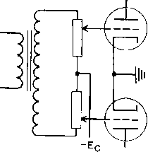 Fig. 129. Input transformer driving push-pull grids. Example (d). Input Transformer, To terminate a 500-ohm line and apply input to push-pull class A grids as in Fig. 129. Primary voltage is 2.0 volts. Frequency range 100 to 5,000 cycles. Step-up ratio 1:20. No direct current flows in either primary or secondary winding. Nickel-iron laminations are used. Refer to Fig. 57 for dimension symbols and winding arrangement. Ac = 0.5 sq in. Ic = 4.5 in. Permeabihty (initial value) = 5,000. Coil mean turn 4.5 in. Window 0.578 in. Primary 400 turns No. 30 single enamel wire. Secondary 8,000 turns No. 40 single enamel wire (total). Primary layers 7; layer paper 0.0015 in. Secondary layers 44; layer paper 0.0007 in. Vertical space factor 0.9. b = 0.75 in. с = 0.008 in. 3.2 X (8,000)2 X 0.5 X 10 Secondary OCL = 0.0005 + 4.5 5,000 Secondary leakage inductance 10.6 X (8,000)2 4 5 X (4 X 0.008 + 0.578) 730 henrys with smallest possible air gap (per Table IX, p. 99). 540 henrys with average gap = 0.001 in. = 0.62 henry 4 X 0.75 X 10 1 See Reactance Chart, by H. A. Wheeler, Proc. LR.E., 38, 1395 (December, 1950). Total secondary capacitance = 127 Mjuf With the primary winding located at audio ground on the secondary, there is virtually zero winding-to-winding capacitance. Secondary-to-core capacitance is based on a coil form Мб in. thick. Total secondary load resistance = 500 X (20) = 200,000 ohms. Based on inductance with 0.001-in. gap, Xn = 339,000 ohms and X/Ri = 1.7. Response is 0.3 db down, in Fig. 108. Resonance frequency of 0.62 henry and 127 Ujuf is 18,000 cycles and Xc = 70,000 ohms. В = Xc/Ri = 0.35. f/fr = 5,000/18,000 = 0.28. Response is 0.6 db down at 5,000 cycles (from Fig. 109). Example (b). Interstage Transformer. In interstage coupling the impedance level is high, to maintain both high load impedance and high grid excitation in the following stage. The limit on the secondary side is the highest resistance which affords grid circuit stability. There is no impedance limit on the primary side except that imposed by transformer design. Usually a 1:1 ratio is about optimum. A step-down ratio gives less voltage on the following grid. A step-up ratio reflects the secondary load into the plate circuit as a lower impedance. This reduces the voltage gain, especially with pentodes which have high plate resistance compared to load resistance. Under this condition, equation 58 becomes Cp/eg = fxZb/rp = OmZb (76) or the voltage gain is proportional to load impedance. Interstage transformers commonly have many turns and high OCL. Suppose that a transformer is required to connect a 6SK7 tube to a 6L6 operating class A with 10 volts rms on the grid over a frequency range of 300 to 3,000 cycles. 6L6 grid resistance is 90,000 ohms, which is to be reflected into the 6SK7 plate circuit as a 90,000-ohm load. Hence a 1:1 turns ratio is used. 6SK7 plate current is 10 ma. The same core as in Example (a) is used, except that here it is made of sihcon steel, and the stacking is reduced so that Ac is 0.32 sq in. Primary and secondary windings are single sections; with the primary start lead connected to 6SK7 plate and secondary finish lead connected to 6L6 grid. This leaves adjacent turns in both these windings at zero audio potential, and effective primary-secondary capacitance is zero. Capacitances: , . .1 0-225 X 4.5 X 0.75 X 3 X 0-9 Secondary layer-to-layer =--------оХЗОбГ+оУоШб- = Ditto referred to whole secondary = X 1.33 X 0.977 = 51 fiiif Primary layer-to-layer, referred to secondajy < 1 Tube input capacitance - 25 AVinding-to-core capacitance = 40 Stray capacitance = 10 Вт = 7,805 gauss. From Fig. 70, = 1,100. 3.2 X (6,600)2 X Q 3g X 10-8 UiJL ---- = 55 henrys. + MOO , 10.6 X (6,600)2 X 3.8(2 X 0.008 + 0.578) , , , Leakage L =-q --1-4 henrys. Capacitances: . , - 0.225 X 3.3 X 0.75 X 3 jrrimary layer-to-layer - - -= 1,120 jujuf. 0.0015 a J 1 .1 0.225 X 4.2 X 0.75 X 3 Secondary layer-to-layer =-ттт^тттт-= 1;415 nt U.0015 Referred to the whole winding, the capacitances are 1,120 X 4 X 0.973 37 X 3 1,415 X 4 X 0.973 = 40/iiu 37 X 3 = 50 Primary-core С =44 Secondary-core С =14 Tube capacitances = 17 Stray capacitances = 10 Total capacitance = 175 njii fr = 10 kc. X = 90,000, D = 1, and response is 1 db down at 3,000 cycles (from Fig. 127). Xn/R2 = 6.28 X 300 X (55/90,000) = 1.04. Figure 118 shows a Z/R2 of 0.72; therefore the response is 3 db down at 300 cycles. Primary turns = secondary turns = 6,600 turns No. 40 enamel wire. Primary and secondary layers = 37. Primary mean turn = 3.3 in. Secondary mean turn = 4.2 in., Ig = 0.005 in. 0.6 X 6,600 X 0.010 Bdc =--= 7,750 gauss. - 3>49 X 10 X 10 ~ 300 X 0.32 X 6,600 ~ 6. AMPLIFIER CIRCUITS Amplifier applications may require control of hum, distortion, or frequency response beyond the limits of practical transformer design. Sometimes the additional performance is obtained by designing extra large transformers; this is usually an expensive procedure. Sometimes extra features can be incorporated into the transformers without marked increase in size. At other times additional circuits are used either preceding or in conjunction with the amplifier. In this chapter several devices for obtaining special performance are considered. Transformer and amplifier design both are affected by them to a marked degree. 73. Inverse Feedback. If part of the output of an amplifier is fed back to the input in such a way as to oppose it, the ripple, distortion, and frequency response deviations in output are reduced. The amplifier gain is reduced also, but with the availability of high-gain tubes an extra stage or two compensates for the reduction in gain caused by inverse feedback, and the improvement in performance usually justifies it. In the amplifier of Fig. 130, a network is shown connected to out- AMPLIFIER FEEDBACK NETWORK IB Fia. 130. Voltage feedback. put voltage Eo; part of this output is fed back so that the input to the amplifier is E2 = El- /ЗЕа (77) Here is the portion of Eq which is fed back. If a is the voltage ampli- fication of the ampHfier and Er and Eh are the ripple and harmonic distortion in the output without feedback, and a, Er, and Е'н are the same properties with feedback, the following equations hold, if a, Er, and Eh are assumed to be independent: Without feedback, Eo. = aE2 Л-ЕвЛ-Ен (78) With feedback, 0 = ccEi + Er + Wh (79) From these equations it can be shown that a =-- - (80) 1 -P aQ ajS En Eh Eh = - - - (82 1 + /3 With high-gain amplifiers and large amounts of feedback, the output ripple and harmonic distortion can be made astonishingly small. Likewise the frequency response can be made flat, even with mediocre transformers. Inverse feedback is not used in class С amplifiers, because the output and input are not linearly related. Incidental effects in the amplifier, like distributed capacitance and leakage inductance, have to be carefully matched in the inverse feedback network so that the phase shift around the loop does not become too large. If it reaches ISO, feedback is regenerative, so that the amplifier may become an oscillator with a frequency determined by the circuit constants. Nyquist has shown that oscillation does not take place so long as the gain X feedback product а/З is less than unity at the frequencies for which the phase shift is 180°. In a plot of ot. made on the complex plane, the requirement for stability is that the curve of must not enclose the point 1, 0, with the sign of considered opposite to that of a. Both gain a and feedback 8 are ratios of voltages. Therefore, both may be expressed in decibels and both are complex quantities at some frequencies. Proper care in application is required so that amplifiers with 180° or more phase shift do not oscil- iSee Regeneration Theory, by H. Nyquist, Bell System Tech. J., 11, 126 (January, 1932). late at some frequency outside the pass band. If it is desired to correct for distortion or hum over a frequency range of 30 to 10,000 cycles, the amplifier should have low phase shift over a much wider range, say 10 to 30,000 cycles. In the frequency intervals of 10 to 30 cycles and 10,000 to 30,000 cycles, both the amplification and the feedback should taper off gradually to prevent oscillations. Low phase-shift amplifiers benefit most from inverse feedback. Feedback in such amplifiers reduces size or improves performance, including phase shift. Transformer phase shift, therefore, is a vital (Л UJ 0 ш (Л 60 -ч
10.0 Fig. 131. Transformer-coupled amplifier low-frequency phase shift. property in feedback amplifiers and may take precedence over frequency response in some instances. Phase shift at low and high frequencies is shown in Figs. 131 and 132 for transformer-coupled stages. At high frequencies, 180° phase shift is possible whereas at low frequencies but 90° is possible. In a resistance-coupled amplifier, only 90° phase shift occurs at either low or high frequencies. Partly for this reason, partly because less capacitance is incidental to resistors than to transformers and good response is maintained up to higher frequencies, it is in resistance-coupled amplifiers that inverse feedback is generally employed. But if the distortion of a final stage is to be reduced, transformer coupling is involved. It is preferable to derive the feedback voltage from the primary side of the output transformer. This is equivalent to tapping between Ri and Xj, in Fig. 132, where the phase shift is much less. The transformer must still present a fairly high impedance load to the output tube throughout the marginal frequency intervals to permit gradual decrease of both amplification and feedback. Current feedback is effected in the circuit of Fig. 133 by removing capacitor C. This introduces degeneration in the cathode resistor circuit, which accomplishes the same thing as the bucking action of й 20 a: о iij a 40 I I 60 <n 80 < w 100 120 140
FREQUENCY Fig. 132. Transformer-coupled amplifier high-frequency phase shift. voltage feedback. It is less affected by phase shift and consequently is used with transformer-coupled amplifiers. 74. Cathode Follower. The circuit of Fig. 134 is known as a cathode follower. Here the anode is connected to the high-voltage supply Ев without any intervening impedance, so that for alternating currents it 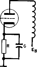 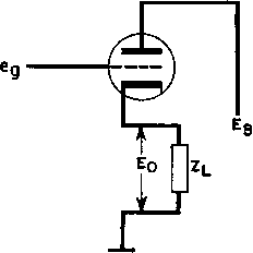 Fig. 133. Cathode bias. Fig. 134. Cathode follower. is essentially grounded. Grid voltage must be great enough to include the output Eq in addition to the normal grid-to-cathode voltage at min- However, the grid power is still the same as it would be 1 ... 15 16 17 18 19 20 21 ... 38 |
||||||||||||||||||||||||||||||||||||||||||||||||||||||||||||||||||||||||||||||||||||||||||||||||||||||||||||||||||||||||||||||||||||||||||||||||||||||||||||||||||||||||||||||||||||||||||||||||||||||||||||||||||||||||||||||||||||||||||||||||||||||||||||||||||||||||||||||||||||||||||||||||||||||||||||||||||||||||||||||||||||||||||||||||||||||||||||||||||||||||||||||||||||||||||||||||||||||||||||||||||||||||||||||||||||||||||||||||||||||||||||||||||||||||||||||||||||||||||
|
© 2026 AutoElektrix.ru
Частичное копирование материалов разрешено при условии активной ссылки |