 |
 |
 |
| Главная Журналы Популярное Audi - почему их так назвали? Как появилась марка Bmw? Откуда появился Lexus? Достижения и устремления Mercedes-Benz Первые модели Chevrolet Электромобиль Nissan Leaf |
Главная » Журналы » Transformer elementary form 1 ... 27 28 29 30 31 32 33 ... 38 10. PULSE AND VIDEO TRANSFORMERS 122. Square Waves. Square waves or pulses differ from sine waves in that the front and back sides of the wave are very steep and the top flat. Such pulses are used in the television and allied techniques to produce sharp definition of images or signals. A square wave can be thought of as made up of sine waves of a large number of frequencies starting with, say, audio frequencies and extending into the medium r-f range. The response of a transformer to these frequencies determines the fidelity with which the square wave is reproduced by the transformer. Some pulses are not square, but have sloping sides and a round top, like a half-wave rectifier Aoit-age. Such pulses will not be discussed here, because if a transformer or circuit is capable of reproducing a square wave, it will reproduce a rounded wave at least as well. Square waves can be generated in several ways: sometimes from sine waves by driving a tube into the diode region each cycle. The plate circuit voltage wave form is then different from that of the grid \oltage because the round top of the sine wave has been removed. By repeating this process (called clipping) in several stages, it is possible to produce very square waves, alternately plus and minus, like those of Fig. 225(a). If a voltage ha\ing such a wave form is applied across a capacitor, it causes current to flow in the capacitor only at the vertical edges, as in Fig. 225(b). If a voltage proportional to this current is then successively amplified and clipped at the base, it results in the wave form of Fig. 225(c). Here the negative loops are assumed to be missing, as they could be after single-side amplification. The wave is 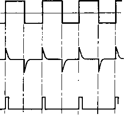 1- (C) Fia. 225. Square waves differentiated and cUpped. again square but of much shorter duration than in Fig. 225(a), and the interval between pulses greatly exceeds the pulse duration. The pulse duration is usually referred to as the pulse width, and the frequency at which the pulses occur is called the repetition rate and is expressed as pulses per second (pps). Common pulse widths lie between 0.5 and 10 microseconds; the intervals between pulses may be between 10 and 1,000 times as long as the pulse width. These values are representative only, and in special cases may be exceeded several-fold. The general wave shape of Fig. 225(c), with short pulse duration compared to the interval between pulses, is the main subject of this chapter. The ratio of peak to average л^oltage or current may be very high, and the rms values appreciably exceed average in such pulses. There are two ways in which the response of any circuit to a square wave can be found. The first of these consists in resolving the pulse into a large number of sine waves of different frequencies, finding the response of the circuit to each frequency and summing up these responses to obtain the total response. This can be formulated by a Fourier integral, but for most circuits the formulation is easier than the solution. An approximation to this method is the arbitrary omission of frequency components having negligible amplitude, and calculation of the circuit response to the relevant frequencies. This approximation has two subjective criteria: the number of frequencies to be retained, and the evaluation of the frequency components for which the circuit has poor response. The second method, which will be used here, consists in finding the transient circuit response to the discontinuities at the front and trailing edges of the square wave. It is possible to reduce the transformer to a circuit amenable to transient analysis, without making any more assumptions than would be necessary for practical design work with the Fourier method. The transient method has the advantage of giving the total response directly, and it can be plotted as a set of curves which are of great convenience to the designer. The major assumption is that one transient disappears before another begins. If good square wave response is obtained, this assumption is justified. Analyses are given of the influence of iron-core transformer and choke characteristics on pulse wave forms. In all these analyses the transformer or choke is reduced to an equivalent circuit; this circuit changes for different wave forms, portions of a wave form, and modes of operation. Initial conditions, resulting formulas, and plots of the formulas for design convenience are given for each case. Formulas may be verified by the methods of operational calculus. 123. Transformer-Coupled Pulse Amplifiers. The analysis here given is for a square- or flat-topped pulse impressed upon the transformer by some source such as a vacuum tube, a transmission line, or 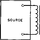 Fig. 226. Flat-topped pulse. Fig. 227. Transformer coupling. even a switch and battery. Such a pulse is shown in Fig. 226, and a generalized circuit for the amplifier is shown in Fig. 227. The equivalent circuit for such an amphfier is given in Fig. 228. At least this is the circuit which applies to the front edge a of the pulse shown in Fig. 226 as rising abruptly from zero to some steady value E. This change is sudden, so that the transformer OCL can be considered as presenting infinite impedance to such a change, and is omitted in Fig. 228. Transformer leakage inductance, though, has an appreciable influence and is shown as inductance L in Fig. 228. Resistor R- of Fig. 228 repre- FiG. 228. Equivalent circuit. sents the source impedance; transformer winding resistances are generally negligible compared to the source impedance. Winding capacitances are showm as Ci and C2 for the primary and secondary windings, respectively. The transformer load resistance, or the load resistance into which the amplifier works, is shown as R2. All these values are referred to the same side of the transformer. Since there are two capacitance terms Ci and C2, it follows that, for any deviation of the ransformer turns ratio from unity, one or the other of these becomes predominant. Turns ratio and therefore voltage ratio affect these capacitances, as discussed in Chapter 5; for a step-up transformer, Ci may be neglected, and, for a step-doAvn transformer, С2 may be neglected. The discussion here will be confined first to the step-up case. 124. Front-Edge Response. The step-up transformer is illustrated by Fig. 229. When the front of the wave (Fig. 226) is suddenly im- Fig. 229. Circuit for step-up transformer. pressed on the transformer, it is simulated by the closing of switch S. At this initial instant, voltage e across R2 is zero, and the current from battery E is also zero. This furnishes two initial conditions for equation 128, which expresses the rate of rise of voltage e from zero to its final steady value Ea = EUi/iRi + R2): Rl -\- R2 L mi - 7712 - 1 + THi - Ш2У (128) where mi, m2 = -m(l d= Vl - 1/ki). Figure 230 shows the rate of rise of the transformed pulse for Й1 - 0 and Fig. 231 for Ri = R2. In hard-tube modulators, source resistance is comparatively small and approaches Й1 - 0. Line-type modulators are usually designed so that Ri = R2. The scale of abscissas for these curves is not time but percentage of the time constant T of the transformer. The equation for this time constant is given in Figs. 230 and 231. It is a function of leakage inductance and of capacitance Co. The rate of voltage rise is governed by another factor ki, which is a measure of the extent to луЬ1сЬ the circuit is damped. The relation of this factor ki and the various con- 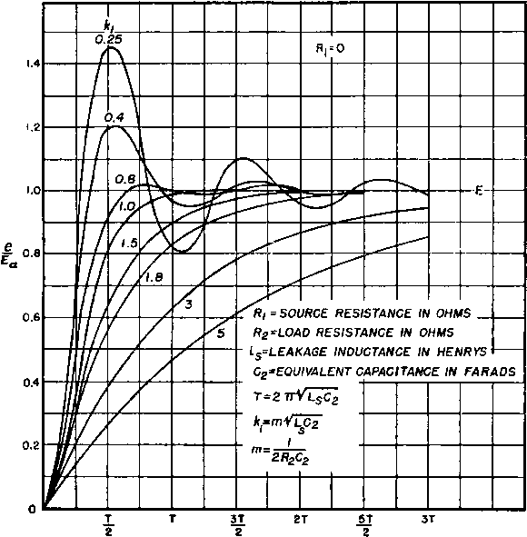 Fig. 230. Influence of transformer constants on front edge of pulse {R = 0). For equivalent circuit see Fig. 229. oscillation can be tolerated, the wave rises up faster than if no oscillation is present. Yet, if the circuit is damped very little, the oscillation may reach a maximum initial voltage of twice steady-state voltage Ea, and usually such high peaks are objectionable. The values for fci given in these figures are those which fall Avithin the most practicable range. Time required for pulse Aoltage to reach 90 per cent of Ea is given in Fig. 232. stants of the transformer is given directly in Figs. 230 and 231. The greater the transformer leakage inductance and distributed capacitance, the slower is the rate of rise, although the effect of and R2 is important, for they affect the damping factor ki. If a slight amount of 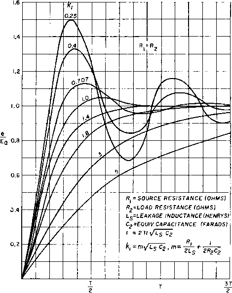 Fig. 23L Influence of transformer constants on front edge of pulse {R = R). 125. Response at the Top of the Pulse. Once the pulse top is reached, Ea is dependent on the transformer OCL for its maintenance at this value. If the pulse stayed on indefinitely at the value Ea, an infinite inductance would be required to maintain it so, and of course this is not practical. There is ahvays a droop at the top of such a pulse. The equivalent circuit during this time is shown in Fig. 233. Here the inductance L is the OCL of the transformer, and and R2 remain the same as before. Since the rate of voltage change is relatively small during this period, capacitances Ci and C2 disappear. Also, since leakage inductance usually is small compared with the OCL, it is-neglected. At the beginning of the pulse, the voltage e across R2 is assumed to be at steady value Ea which is true if the voltage rise is rapid. Curves for the top of the wave are shown b Fig. 234. Several curves are given; they represent several types of pulse amplifiers ranging from a pentode in which R2 is one-tenth of Й1, to an amplifier in which load resistance is infinite and output power is zero. In the latter curve, the о о о < ш о: о о ш ? 2 I- g о Fig. 232. Time required to reach 90 per cent of final voltage. Ioltage e has for its initial value the voltage of the source. All the curves are exponential, having a common point at 0, 1. Abscissas are the product of time т and Ri/Lg, time т being the duration of the pulse between points a and b in Fig. 226. The greater the inductance Le the less the deviation from constant voltage during the pulse. 126. Trailing-Edge Response. At instant b in Fig. 226, it is assumed that the switch *S in Fig. 233 is opened suddenly. The equivalent circuit now reverts to that shown in Fig. 235, in which Le is the OCL, and is total capacitance referred to the primary. Figure 235 illustrates the decline of pulse voltage after instant b (Fig. 226), the equation for which is: 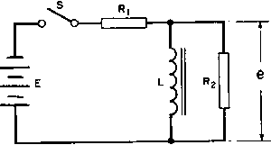 Fig. 233. Circuit for top of pulse. (129) (mi + 2Am)e - (mg + 2Am)e -] mi - m2 where mi, m2 = -m(l ± Vl - l/k ), m. = }RiCdj and other terms are defined in Fig. 235. Abscissas are time in terms of the time constant determined b OCL and capacitance Cd- Ratio on these curves has a different meaning, and time constant T is greater than in Fig. 230, but with low capacitance is high and the curves with higher values of /сз drop rapidly. The slope of the trailing edge can be kept within tolerable limits, provided that the capacitance of the transformer is small enough. Accurate knowledge of this capacitance is therefore important. Measurement and evaluation of transformer capacitance should be made as in Chapters 5 and 7. 1.0 0.Э 0.8 0.7 0.6 0.5 0.4 0.3 0.2 0.1 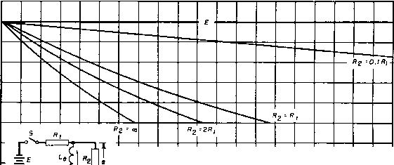 Le=O.C.L. IN MICROHENRYS Г'PULSE WIDTH IN Micttosecortos Rl SOURCE RESISTANCE IN OHMS RZLOAD RESISTANCE Ш OHMS I.г Fig. 234. Droop at top of pulse transformer output voltage. If the transformer has appreciable magnetizing current, the shape of the trailing edge is changed. The greater the magnetizing current, the more pronounced the negative voltage backswing. The ordinates at the left of Fig. 235 are given in terms of the voltage E ., at instant a, as if there were no droop at the top of the pulse. These curves apply when there is droop, but then the ordinates should be multiplied by the fraction of Ea to which the voltage has fallen at the end of the pulse. Magnetizing current at the end of the pulse is in = {EJmL){l - (130) where m = RR/iRi + R2)L (see Fig. 233) t = pulse duration in seconds L ~ primary OCL in henrys Magnetizing current can be expressed as a fraction Д of the primary load current /, or Д = iu/I- For any R1/R2 ratio, A = [{Ri + R2)/Ri] 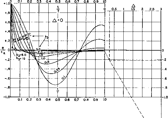 To find e/Ea a.i any time t/t, кз and Д: (a) Take initial e/Ea for the appropriate t/t and к from left-hand chart; project this point to the right to obtain intersection with Л = 0 line. I ta,ke second e/Ea at the same t/t and кз from right-hand chart; project to the left to obtain intersection with Д = 3 Urie. (c) Through these intersections draw a straight line. (d) Drop given value of Д to intersect this line; project horizontally to obtain actual e/Ea. Example shown dotted is for кз = 3.84, t/t = 0.5, and Д = 0.256. .Answer e/Ea = -0.21. Ea = Volts at end of pulse = Primary ocl cd = Primary equivalent capacitance Rl = Primary equivalent resistance , V ljcd equiv. circuit t = 2vucd Magnetizing current Load current Fig. 235. Interpolation chart for X voltage droop at point Ъ (Fig. 226), or E/E, = 1 - RiA/{Ri + ад (131) where Ea = voltage at point a (Fig. 226), and E = voltage at point 6. This equation gives the multiplier for finding the actual trailing-edge voltage from the backswing curve parameters in Fig. 235. With increasing values of Д the backswing is increased, especially for the damped circuits corresponding to values of fcg 1.0. The same is also true for lower values of ks, but with diminishing emphasis, so that in Fig. 235 exciting current has less influence on the oscillatorv 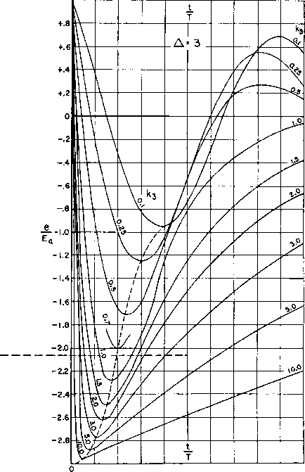 0.1 0.2 0.3 0.4 0.5 0.6 0.7 0, pulse transformer backswing. 8 0.9 1.0 backswings. These afford poor reproduction of the original pulse shape, but occasionally large backswing amplitudes are useful, as mentioned in Section 137. Equation 129 is plotted at the left of Fig. 235 for Д 0, and at the right of Fig. 235 for Д - 3. Instructions are given under Fig. 235 for finding the backswing in terms of Ea by interpolation for 0 < Д < 3, and for given values of fcg and t/T. This chart eliminates the labor of solving equation 129 for a given set of circuit conditions. Elements Lg, Cjj, and Ri in Fig. 235 sometimes include circuit components in addi- 0 01 0.2 0.3 0.4 0.5 0.6 0 7 0 8 0 9 1.0 1 ... 27 28 29 30 31 32 33 ... 38 |
|
© 2026 AutoElektrix.ru
Частичное копирование материалов разрешено при условии активной ссылки |