 |
 |
 |
| Главная Журналы Популярное Audi - почему их так назвали? Как появилась марка Bmw? Откуда появился Lexus? Достижения и устремления Mercedes-Benz Первые модели Chevrolet Электромобиль Nissan Leaf |
Главная » Журналы » Absorbing materialorganic polymer 1 2 3 4 ... 55 absorbing material Organic polymer that undergoes chemical change when exposed to uUraviolet light. The photoresist is exposed to ultraviolet light through the photomask as indicated in Figure 0.2. The photoresist is then developed in a chemical solution. The developer is used to remove the unwanted portions of the photoresist and generate the appropriate patterns on the silicon. The photomasks and photolithography process is critical in that it determines how small the devices can be made. Instead of using ultraviolet light, electrons and x-rays can also be used to expose the photoresist. Etching After the photoresist pattern is formed, the remaining photoresist can be used as a mask, so that the material not covered by the photoresist can be etched. Plasma etching is now the standard process used in 1С fabrication. Typically, an etch gas such as chlorofluorocarbons are injected into a low-pressure chamber A plasma is created by applying a radio-frequency voltage between cathode and anode terminals. The silicon wafer is placed on the cathode. Positively charged ions in the plasma are accelerated toward the cathode and bombard the wafer normal to the surface. The actual chemical and physical reaction at the surface is complex, but the net result is that silicon can be etched anisotropically in very selected regions of the wafer. If photoresist is applied on the surface of silicon dioxide, then the silicon dioxide can also be etched in a similar way. Diffusion A thermal process that is used extensively in 1С fabrication is diffusion. Diffusion is the process by which specific types of impurity atoms can be introduced into the silicon material. This doping process changes the conductivity type of the silicon so that pn junctions can be formed. (The pn junction is a basic building block of semiconductor devices.) Silicon wafers are oxidized to form a layer of silicon dioxide and windows are opened in the oxide in selected areas using photolithography and etching as just described. The wafers are then placed in a high-temperature furnace (about 1100 C) and dopant atoms such as boron or phosphorus are introduced. The dopant atoms gradually diffuse or move into the silicon due to a density gradient. Since the diffusion process requires a gradient in the concentration of atoms, the final concentration of jcxii Prologue diffused atoms is nonlinear, as shown in Figure 03. When the wafer is removed from the furnace and the wafer temperature returns to voom temperature, the diffusion coefficient of the dopant atoms is essemially zero so that the dopant atoms are then fixed in the silicon material. Ion Implantation A fabrication process that is an alternative to high-temperature diffusion is ion implantation. A beam of dopant ions is accelerated to a high energy and is directed at the surface of a semiconductor. As the ions enter the silicon, they collide with silicon atoms and lose energy and finally come to rest at some depth within the crystal. Since the collision process is statistical in nature, there is a distribution in the depth of penetration of the dopant ions. Figure 0.4 shows such an example of the implantation of boron into silicon at a particular energy. Two advantages of the ion implantation process compared to diffusion are (I) the ion iinplantation process is a low temperature process and (2) very well defined doping layers can be achieved. Photoresist layers or layers of oxide can be used to block the penetration of dopant atoms so that ion implantation can occur in very selected regions of the silicon. О о Eh о Diffused impurities Background doping Surface Distance Figure 0.31 Final concentration of diffused impurities into the surface of a semiconductor.  Surface Distance (Projected range) Figure 0,41 Final concentration of ion-implanted boron into silicon. One disadvantage of ion implantation is that the silicon crystal is damaged by the penetrating dopant atoms because of collisions between the incident dopant atoms and the host siHcon atoms. However, most of the damage can be removed by thermal annealing the silicon at an elevated temperature. The thermal annealing temperature, however, is normally much less that the diffusion process temperature. Metallization Bondings and Packaging After the semiconductor devices have been fabricated by the processing steps discussed, they need to be connected to each other to form the circuit. Metal films are generally deposited by a vapor deposition technique and the actual interconnect lines are formed using photolithography and etching. In general, a protective layer of silicon nitride is finally deposited over the entire chip. The individual integrated circuit chips are separated by scribing and breaking the wafer. The integrated circuit chip is then mounted in a package. Lead bonders are finally used to attach gold or aluminum wires between the chip and package terminals. Summary: Simplified Fabrication of a pn Junction Figure 0.5 shows the basic steps in fomiing a pn junction. These steps involve some of the processing described in the previous paragraphs.  [.Start with 15 type substrate SiO,  2- Oxidize surface  3. Apply photoresist over SiOi SiO:, UV light  3. Expose photoresist through photomask Exposed PR removed  4. Remove exposed photoresist 77\ U77\ SiOs etched 5. Etch exposed SiOi Ion implant or diffuse p-regions  6. Ion implant or diffuse boron into silicon Apply Al 771 f-TTte 7, Remove PR and sputter Al on surface Al contacts  8. Apply PR, photomask, and etch to form Al contacts over p-regions Figure 0.5 I The basic steps in forming a pn junction. с Н А Т Б R The Crystal Structure of SoUds PREVIEW This text deals with the electrical properties and characteristics of semiconductor materials and devices. The electrical properties of solids are therefore of primary interest. The semiconductor is in general a single-crystal material. The electrical properties of a single-crystal material are determined not only by the chemical composition but also by the arrangement of atoms in the solid; this being true, a brief study of the crystal structure of solids is warranted. The forination, or growth, of the single-crystal material is an important part of semiconductor technology. A short discussion of several growth techniques is included in this chapter to provide the reader with some of the terminology that describes semiconductor device structures. This introductory chapter provides the necessary background in single-crystal materials and crystal growth for the basic understanding of the electrical properties of semiconductor materials and devices. 1.1 I SEMICONDUCTOR MATERIALS Semiconductors are a group of materials having conductivities between those of metals and insulators. Two general classifications of semiconductors are the elemental semiconductor materials, found in group IV of the periodic table, and the compound semiconductor materials, most of which are formed from special combinations of group 111 and group V elements. Table 1.1 shows a portion of the periodic table in which the more common semiconductors are found and Table 1.2 lists a few of the semiconductor materials. (Semiconductors can also be formed from combinations of group П and group VI elements, but in general these will not be considered in this text.) The elemental materials, those that are composed of single species of atoms, are silicon and germanium. Silicon is by far the most common semiconductor used in integrated circuits and will be emphasized to a great extent. Table IД 1 A portion of the periodic table
Table L2 I A list of some semiconductor materials Elemental semiconductors Silicon Germanium Compound semiconductors
The two-element, or binary, compounds such as gallium arsenide or gallium phosphide are formed by combining one group III and one group V element. Gallium arsenide is one of the more common of the compound semiconductors. Its good optical properties make it useful in optical devices. GaAs is also used in specialized applications in which, for example, high speed is required. We can also form a three-element, or ternary, compound semiconductor. An example is Al,vGa r As, in which the subscript x indicates the fraction of the lower atomic number element component. More complex semiconductors can also be formed that provide flexibility when choosing material properties. 1.2 I TYPES OF SOLIDS Amorphous, polycrystalline, and single crystal are the three general types of solids. Each type is characterized by the size of an ordered region within the material. An ordered region is a spatial volume in which atoms or molecules have a regular geometric arrangement or periodicity. Amorphous materials have order only within a few atomic or molecular dimensions, while polycrystalline materials have a high degree   Figure 1.1 I Schematics of three general types of crystals: (a) amorphous, (b) polycrystalline, (c) single crystal. of order over many atomic or molecular dimensions. These ordered regions, or single-crystal regions, vary in size and orientation with respect to one another The single-crystal regions are called grains and are separated from one another by grain boundaries- Single-crystal materials, ideally, have a high degree of order, or regular geometric periodicity, throughout the entire volume of the material. The advantage of a single-crystal material is that, in general, its electrical properties are superior to those of a nonsingle-crystal material, since grain boundaries tend to degrade the electrical characteristics. Two-dimensional representations of amoфhous, polycrys-talline, and single-crystal materials are shown in Figure 1, F 1.3 I SPACE LATTICES Our primary concern will be the single crystal with its regular geometric periodicity in the atomic arrangement. A representative unit, or group of atoms, is repeated at regular intervals in each of the three dimensions to form the single crystal. The periodic arrangement of atoms in the crystal is called the lattice. 1.3.1 Primitive and Unit Cell We can represent a particular atomic array by a dot that is called a lattice point. Figure 1.2 shows an infinite two-dimensional array of lattice points. The simplest means of repeating an atomic array is by translation. Each lattice point in Figure 1.2 can be translated a distance a] in one direction and a distance Z?i in a second nonco-linear direction to generate the two-dimensional lattice. A third noncolinear translation will produce the three-dimensional lattice. The translation directions need not be peфendicular. Since the three-dimensional lattice is a periodic repetition of a group of atoms, we do not need to consider the entire lattice, but only a fundamental unit that is being repeated. A unit cell is a small volume of the crystal that can be used to reproduce the entire crystal. A unit cell is not a unique entity. Figure 1.3 shows several possible unit cells in a two-dimensional lattice.   T  Figure 1.21 Two-dimensional representation of a single-crystal lattice. Figure 1.3 I Two-dimensional representation of a single-crystal lattice showing various possible unit cells.  Figure 1.4 f A generalized primidve unit cell. The unit cell A can be translated in directions сь and /?2 the unit cell В can be translated in directions щ and by, and the entire two-dimensional lattice can be constructed by the translations of either of these unit cells. The unit cells С and D in Figure 13 can also be used to construct the entire lattice by using the appropriate translations. This discussion of two-dimensional unit cells can easily be extended to three dimensions to describe a real single-crystal material. A primitive cell the smallest unit cell that can be repeated to form the lattice. In many cases, it is more convenient to use a unit cell that is not a primitive cell. Unit cells may be chosen that have orthogonal sides, for example, whereas the sides of a primitive cell may be nonorthogonal. A generalized three-dimensional unit cell is shown in Figure 1.4. The relationship between this cell and the lattice is characterized by three vectors a, b, and c, which need not be peфendcular and which may or may not be equal in length. Every equivalent lattice point in the three-dimensional crystal can be found using the vector r раЛ-цЬЛ- sc (1.1) where p, q, and .s are integers. Since the location of the origin is arbitrary, we will let p,q, and л be positive integers for simplicity. 1,3.2 Basic Crystal Structures Before we discuss the semiconductor crystal, let us consider three crystal structures and determine some of the basic characteristics of these crystals. Figure 1.5 shows the simple cubic, body-centered cubic, and face-centered cubic structures. For these simple structures, we may choose unit cells such that the general vectors a, b, and с are perpendicular to each other and the lengths are equal. The simple cubic (sc) structure has an atom located at each corner; the body-centered cubic (bcc) structure has an additional atom at the center of the cube; and the face-centered cubic (fee) structure has additional atoms on each face plane. By knowing the crystal structure of a material and its lattice dimensions, we can determine several characteristics of the crystal. For example, we can determine the volume density of atoms. 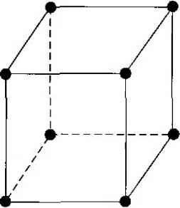   Figure 1.5 I Three lattice types: (a) simple cubic, (b) body-centered cubic, (c) face-centered cubic. Objective To find the volume density of atoms in a crystal. Consider a single-crystal material that is a body-centered cubic with a lattice constant a - 5 A = 5 X 10~ cm. A corner atom is shared by eight unit cells which meet at each corner so that each comer atom effectively contributes one-eighth of its volume to each unit cell. The eight comer atoms then contribute an equivalent of one atom to the unit cell. If we add the body-centered atom to the comer atoms, each unit cell contains an equivalent of two atoms. Solution The volume density of atoms is then found as Density = 2 atoms (5 X 10- y 3 1.6 X 10 - atoms per cm Comment The volume density of atoms just calculated represents the order of magnitude of density for most materials. The actual density is a function of the crystal type and crystal structure since the packing density-number of atoms per unit cell-depends on crystal structure. EXAMPLE 1.1 TEST YOUR UNDERSTANDING о Е1Л The lattice constant of a face-centered-cubic structure is 4.75 A. Determine the volume density of atoms. Q m3 --Q] x eAT suy) EL2 The volume density of atoms for a simple cubic lattice is 3 x 10 cm . Assume that the atoms are hard spheres with each atom touchiig its nearest neighbor. Determine the lattice constant and the radium of the atom. (V 19* I = V ZZT = пу) 1.3.3 Crystal Planes and Miller Indices Since real crystals are not infinitely large, they eventually terminate at a surface. Semiconductor devices are fabricated at or near a surface, so the surface properties may influence the device characteristics. We would like to be able to describe these surfaces in terms of the lattice. Surfaces, or planes through the crystal, can be described by first considering the intercepts of the plane along the a, b, and с axes used to describe the lattice. EXAMPLE 1.2 Objecrive To describe the plane shown in Figure 1.6- (The lattice points in Figure L6 are shown along the a, b, and с axes only)  Figure L6 IA representative crystal-lattice plane. Solution From Equation (1.1), the intercepts of the plane correspond to = 3, = 2, and 5 = L Now write the reciprocals of the intercepts, which gives Multiply by the lowest common denominator, which in this case is 6, to obtain (2, 3, 6). The plane in Figure 1.6 is then referred to as the (236) plane. The integers are referred to as the Miller indices. We will refer to a general plane as the Qikl) plane. Comment We can show that the same three Miller indices are obtained for any plane that is parallel to the one shown in Figure 1.6. Any parallel plane is entirely equivalent to any other. Three planes that are commonly considered in a cubic crystal are shown in Figure 1.7. The plane in Figure 1.7a is parallel to the b and с axes so the intercepts are given as /? = 1, <7 = oo, and 5 - 00. Taking the reciprocal, we obtain the Miller indices as (1, 0, 0), so the plane shown in Figure L7a is referred to as the (100) plane. Again, any plane parallel to the one shown in Figure L7a and separated by an integral    Figure 1.7 I Three lauice planes: (a) (100) plane, (b) (110) plane, (c) (111) plane. number of lattice constants is equivalent and is referred to as the (100) plane. One advantage to taking the reciprocal of the intercepts to obtain the Miller indices is that the use of infinity is avoided when describing a plane that is parallel to an axis. Tf we were to describe a plane passing through the origin of our system, we would obtain infinity as one or more of the Miller indices after taking the reciprocal of the intercepts. However, the location of the origin of our system is entirely arbitrary and so, by translating the origin to another equivalent lattice point, we can avoid the use of infinity in the set of Miller indices. For the simple cubic structure, the body-centered cubic, and the face-centered cubic, there is a high degree of symmetry. The axes can be rotated by 90in each of the three dimensions and each lattice point can again be described by Equarion (1.1) as г = pa + qb + sc (Fl) Each face plane of the cubic structure shown in Figure 1.7a is entirely equivalent. These planes are grouped together and are referred to as the {100} set of planes. We may also consider the planes shown in Figures 1.7b and 1.7c. The intercepts of the plane shown in Figure 1.7b are = 1, = 1, and s = oo. The Miller indices are found by taking the reciprocal of these intercepts and, as a result, this plane is referred to as the (110) plane. In a similar way, the plane shown in Figure 1.7c is referred to as the (111) plane. One characteristic of a crystal that can be determined is the distance between nearest equivalent parallel planes. Another characteristic is the surface concentration of atoms, number per square centimeter (/cnrX that are cut by a particular plane. Again, a single-crystal semiconductor is not infinitely large and must terminate at some surface. The surface density of atoms may be important, for example, in determining how another material, such as an insulator, will fit on the surface of a semiconductor material. 1 2 3 4 ... 55 |
|
© 2026 AutoElektrix.ru
Частичное копирование материалов разрешено при условии активной ссылки |