 |
 |
 |
| Главная Журналы Популярное Audi - почему их так назвали? Как появилась марка Bmw? Откуда появился Lexus? Достижения и устремления Mercedes-Benz Первые модели Chevrolet Электромобиль Nissan Leaf |
Главная » Журналы » Absorbing materialorganic polymer 1 ... 8 9 10 11 12 13 14 ... 55 Problems 3.9 Using the parameters in Problem 3.5 and letting a = 5 A, determine the width (in eV) of the allowed energy bands that exist for {a)0 < ka < тт, (Ь)л: < ka < 2jr, (c) In <ka < Зтг, and {d) Зл < ka < Ал, 3.10 Repeat Problem 3.8 using the parameters in Problem 3.6. 3.11 Repeat Problem 3.9 using the parameters in Problem 3.6. 3.12 The bandgap energy in a semiconductor is usually a sUght function of temperature. In some cases, the bandgap energy versus temperature can be modeled by E, = £,(0)---- where Eg (0) is the value of the bandgap energy at Г = 0 K. For silicon, the parameter values are £(0) = 1.170 eV, = 4.73 x 10 eV/K and p = 636 K. Plot E, versus rover the range 0 < 7 < 600 K. In particular, note the value at Г = 300 К. Section 3.2 Electrical Conduction in Solids 3.13 Two possible conduction bands are shown in the E versus к diagram given in Figure 3.34. State which band will result in the heavier electron effective mass; state why. 3.14 Two possible valence bands are shown in the E versus к diagram given in Figure 3.35. State which band will result in the heavier hole effective mass; state why, 3.15 The E versus к diagram for a particular allowed energy band is shown in Figure 3.36. Determine (a) the sign of the effective mass and (/?) the direction of velocity for a particle at each of the four positions shown. ЗЛ6 Figure 3.37 shows the parabolic E versus к relationship in the conduction band for an electron in two particular semiconductor materials. Determine the effective mass (in units of the free electron mass) of the two electrons. 3.17 Figure 3.38 shows the parabolic E versus к relationship in the valence band for a hole in two particular semiconductor materials. Determine the effective mass (in units of the free electron mass) of the two holes. 3.18 The forbidden energy band of GaAs is 1.42 eV. (a) Determine the minimum frequency of an incident photon that can interact with a valence electron and elevate the electron to the conduction band, {b) What is the corresponding wavelength? 3.19 The E versus к diagrams for a free electron (curve A) and for an electron in a semiconductor (curve B) are shown in Figure 3.39. Sketch (a) dE/dk versus к and   В 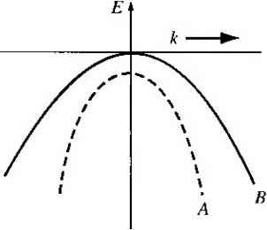 Figure 3.34 I Conduction bands for Problem 3.13. Figure 3.35 I Valence bands for Problem 3.14. CHAPTERS Introductiontothe Quantum Theory of Solids
Figure 3361 Figure for Problem 3.15. 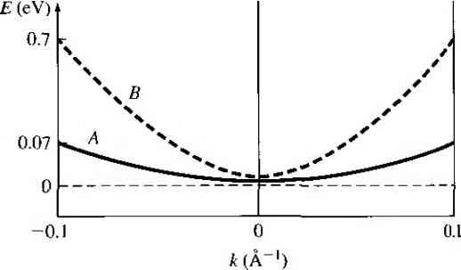 Figure Ъ311 Figure for Problem 3.16. Ey - 0.08 Ey - 0.4 0 k{A-) 0Л  Figure 3.381 Figure for Problem 3.17.
7Т О Figure 3-391 Figure for Problem 3.19. (h) d-E/dk versus к for each curve, (c) What conclusion can you make concerning a comparison in effective masses for the two cases? Section 3.3 Extension to Three Dimensions 3.20 The energy band diagram for silicon is shown in Figure 3.23b. The minimum energy in the conduction band is in the f 100] direction. The energy in this one-dimensional direction near the minimum value can be approximated by E = E{) - E] cosa{k - k[]) where k is the value of к at the tninimum energy. Determine the effective mass of the particle at к = k[) in terms of the equation parameters. Section 3.4 Density of States Function 3.21 Starting with the three-dimensional infinite potential well function given by Equation (3.59) and using the separation of variables technique, derive Equation (3.60). 3.22 Show that Equation (3.69) can be derived from Equation (3.64). 3.23 Determine the total number of energy states in GaAs between E,. and E, -\-кТ at T = 300 K. Problems 101 3.24 Determine the total number of energy states in GaAs between E. and E. - kT at r = 300 K. 3.25 (a) Plot the density of states in the conduction band for silicon over the range Ec E < Ec -\- 0.2 eV. (b) Repeat part (a) for the density of states in the valence band over the range E - 0.2eV < £ < 3.26 Find the ratio of the effecdve density of states in the conduction band at E, -\-kT to the effective density of states in the valence band at Ef. - kT. Section 3.5 Statistical Mechanics 3.27 Plot the Fermi-Dirac probability function, given by Equation (3.79), over the range -0.2 <(E-Ef)< 0.2 eV for (a) T = 200 K, (b) T = 300 K, and (c) T = 400 K. :Qi 3.28 Repeat Example 3.4 for the case when = 10 and Nj =8. 3.29 (a) If Ef = hnd the probability of a state being occupied и\ E = E + kT, (b) If Ef = Я^ find the probability of a state being empty di E = E, - kT. 3.30 Determine the probability that an energy level is occupied by an electron if the state is above the Fermi level by {а)кТ. (b) 5kT. and (c) WkT 3.31 Determine the probability that an energy level is empty of an electron if the state is below the Fermi level by (я) кТ, (b) 5кТ and (с) lOkT 3.32 The Fermi energy in silicon is 0.25 eV below the conduction band energy E. {a) Plot the probability of a state being occupied by an electron over the range E,<E< E, + 2kT. Assume T = 300 K. {b) Repeat part (a) for T = 400 K. 333 Four electrons exist in a one-dimensional infinite potential well of width a = 10 A. Assuming the free electron mass, what is the Fermi energy at Г = 0 K. 334 (a) Five electrons exist in a three-dimensional infinite potential well with all three widths equal to й = 10 A. Assuming the free electron mass, what is the Fermi energy at Г = 0 K. (/?) Repeat part (a) for 13 electrons. 3.35 Show that the probability of an energy state being occupied AE above the Fermi energy is the same as the probability of a state being empty AE below the Fermi level. 3.36 (a) Determine for what energy above Ef (in terms of kT) the Fermi-Dirac probability function is within 1 percent of the Boltzmann approximation, (h) Give the value of the probability funcdon at this energy. 3.37 The Fermi energy level for a particular material at Г 300 К is 6.25 eV. The electrons in this material follow the Fermi-Dirac distribution function, (a) Find the probability of an energy level at 6.50 eV being occupied by an electron, (b) Repeat part (a) if the temperature is increased to 7 = 950 K, (Assume that is a constant.) (c) Calculate the temperature at which there is a 1 percent probability that a state 0.30 eV below the Fermi level will be empty of an electron. 338 The Fermi energy for copper at Г = 300 К is 7.0 eV. The electrons in copper follow the Fermi-Dirac distribution function, (a) Find the probability of an energy level at 7.15 eV being occupied by an electron, (b) Repeat part (a) for T = 1000 K. (Assume that Ef is a constant.) (c) Repeat part (a) for E = 6.85 eV and T = 300 K. {d) Determine the probability of the energy state E = Ef being occupied at Г = 300 К and at Г = 1000 К. 3.39 Consider the energy levels shown in Figure 3.40. Let T = 300 K. (a) If E] - Ef = 0.30 eV, determine the probability that an energy state ai E = E] is occupied by an electron and the probability that an energy state at £ = Я2 is empty, (h) Repeat part (a) if Ef-Ei 0.40 eV. ----------£r l.l2eV Figure 3.40 I Energy levels for Problem 3.39. 3.40 Repeat problem 3.39 for the case when Ei - E2 = 1.42 eV. 3.41 Determine the derivative with respect to energy of the Fermi-Dirac distribution function. Plot the derivative with respect to energy for {a) T =i)KAb)T = 300 K, and (c) T 500 K. 3.42 Assume the Fermi energy level is exactly in the center of the bandgap energy of a semiconductor at Г = 300 К. (a) Calculate the probability that an energy state in the bottom of the conduction band is occupied by an electron for Si, Ge, and GaAs. (b) Calculate the probability that an energy state in the top of the valence band is empty for Si, Ge, and GaAs, 3.43 Calculate the temperature at which there is a 10 probability that an energy state 0.55 eV above the Fermi energy level is occupied by an electron. 3.44 Calculate the energy range (in eV) between (£) = 0.95 and ft{E) = 0.05 for Ef = 7.0 eV and for (a) Г = 300 К and (b) Г = 500 K. READING LIST 1. Kano, K. Semiconductor Devices. Upper Saddle River, NJ: Prentice Hall, 1998. 2. Kittel, C. Introduction to Solid State Physics, 7th ed. Berlin: Springer-Veriag, 1993. 3. McKelvey, J. P. Solid State Physics for Engineering and Materials Science. Malabar, FL.: Krieger, 1993. 4. Pierret, R. F. Semiconductor Device Fundamentals. Reading, MA: Addison-Wesley, 1996. *5. Shock ley, W. Electrons and Holes in Semiconductors. New York: D. Van Nostrand, 1950. 6. Shur, M. Introduction to Electronic Devices. New York: John Wiley and Sons, 1996. *7. Shur, M. Physics of Semiconductor Devices. Englewood Cliffs, NJ: Prentice Hall, 1990- 8. Singh, J. Semiconductor Devices: An Introduction. New York: McGraw-Hill, 1994. 9. Singh, J. Semiconductor Devices: Basic Principles. New York: John Wiley and Sons, 2001. 10. Streelman, B. G., and S. Banerjee. Solid State Electronic Devices, 5th ed. Upper Saddle River, NJ: Prentice-Hall, 2000. 11. Sze, S. M. Semiconductor Devices: Physics and Technology, 2nd ed. New York: John Wiley and Sons, 2001. *12. Wang, S. Fundamentals of Semiconductor Theory and Device Physics. Englewood Chffs, NJ: Prentice Hall, 1988. Е R  The Semiconductor in Equilibrium PREVIEW So far, we have been considering a general crystal and applying to it the concepts of quantum mechanics in order to determine a few of the characteristics of electrons in a single-crystal lattice. In this chapter, we will apply these concepts specifically to a semiconductor material. In particular, we will use the density of quantum states in the conduction band and the density of quantum states in the valence band along with the Fermi-Dirac probability function to determine the concentration of electrons and holes in the conduction and valence bands, respectively. We will also apply the concept of the Fermi energy to the semiconductor material. This chapter deals with the semiconductor in equilibrium. Equilibrium, or thermal equilibrium, implies that no external forces such as voltages, electric fields, magnetic fidds, or temperature gradients are acting on the semiconductor. All properties of the semiconductor will be independent of time in this case. Equilibrium is our starting point for developing the physics of the semiconductor. We will then be able to determine the characteristics that result when deviations from equilibrium occur, such as when a voltage is applied to a semiconductor device. We will initially consider the properties of an intrinsic semiconductor, that is, a pure crystal with no impurity atoms or defects. We will see that the electrical properties of a semiconductor can be altered in desirable ways by adding controlled amounts of specific impurity atoms, called dopant atoms, to the crystal. Depending upon the type of dopant atom added, the dominant charge carrier in the semiconductor will be either electrons in the conduction band or holes in the valence band. Adding dopant atoms changes the distribution of electrons among the available energy states, so the Fermi energy becomes a function of the type and concentration of impurity atoms. Finally, as part of this discussion, we will attempt to add more insight into the significance of the Fermi energy. 4.1 I CHARGE CARRIERS IN SEMICONDUCTORS Current is the rate at which charge flows. In a semiconductor, two types of charge carrier, the electron and the hole, can contribute to a current. Since the current in a semiconductor is determined largely by the number of electrons in the conduction band and the nutuber of holes in the valence band, an important characteristic of the semiconductor is the density of these charge carriers. The density of electrons and holes is related to the density of states function and the Fermi distribution function, both of which we have considered. A qualitative discussion of these relationships will be followed by a more rigorous mathematical derivation of the thermal-equilibrium concentration of electrons and holes. 4.1.1 Equilibrium Distribution of Electrons and Holes The distribution (with respect to energy) of electrons in the conduction band is given by the density of allowed quantum states times the probability that a state is occupied by an electron. This statement is written in equation form as n{E)=g,iE)ME) (4.1) where (E) is the Fermi-Dirac probability function and gJE) is the density of quan- tum states in the conduction band. The total electron concentration per unit volume in the conduction band is then found by integrating Equation (4.1) over the entire conduction-band energy. Similarly, the distribution (with respect to energy) of holes in the valence band is the density of allowed quantum states in the valence band multiplied by the probability that a state \snot occupied by an electron. We may express this as p{E)g,{E)V\- friE)] (4.2) The total hole concentration per unit volume is found by integrating this function over the entire valence-band energy. To find the thermal-equilibrium electron and hole concentrations, we need to determine the position of the Fermi energy Ej, with respect to the bottom of the conduction-band energy and the top of the valence-band energy E.To address this question, we will initially consider an intrinsic .semiconductor. An ideal intrinsic semiconductor is a pure semiconductor with no impurity atoms and no lattice defects in the crystal (e.g., pure silicon). We have argued in the previous chapter that, for an intrinsic semiconductor at 7 = 0 K, all energy states in the valence band are fdled with electrons and all energy states in the conduction band are empty of electrons. The Fermi energy must, therefore, be somewhere between E, and (The Fermi energy does not need to correspond to an allowed energy.) As the temperature begins to increase above 0 K, the valence electrons will gain thermal energy. A few electrons in the valence band may gain sufficient energy to jump to the conduction band. As an electron jumps from the valence band to the conduction band, an empty state, or hole, is created in the valence band. In an intrinsic semiconductor, then, electrons and holes are created in pairs by the thermal energy so 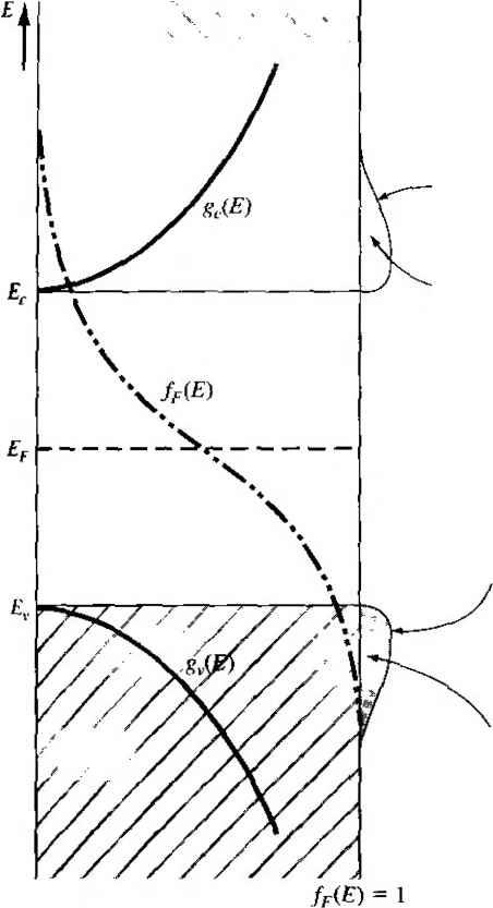 Area = ny-electron concentration 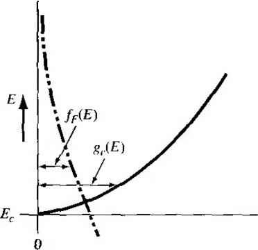 Area - pQ = hole concentration 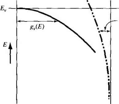 [ 1 - Figure 4.11 (a) Density of states functions, Fermi-Dirac probability function, and areas representing electron and hole concentrations for the case when Ef is near the midgap energy; (b) expanded view near the conduction band energy; and (c) expanded view near the valence band energy. that the number of electrons in the conduction band is equal to the number of holes in the valence band. Figure 4. la shows a plot of the density of states function in the conduction band SciE), the density of states function in the valence band gAE), nd the Fermi-Dirac probability function for T > 0 К when Ef\s approximately halfway between £, and Ev If we assume, for the moment, that the electron and hole effective masses are equal, then gc(E) and gv(£) are symmetrical functions about the midgap energy (the energy midway between E and E). We noted previously that the function fr{E) for E > Efh symmetrical to the function 1 - ffiE) for E < Ef about the energy E= Ef. This also means that the function ffiE) for E = Ef + dE is equal to the function 1 - ffiE) for E - Ef - dE. Figure 4. lb is an expanded view of the plot in Figure 4.1 a showing ff{E) ш gc(E) above the conduction band energy E,.. The product of g,>(£) and ff(E) is iIm distribution of electrons п{Е) in the conduction band given by Equation (4.1). Thij product is plotted in Figure 4Ла. Figure 4.1c is an expanded view of the plot in Fig ure 4.1a showing [1 - /г(Ю] and gviE) below the valence band energy Ei ТЫ product of gu(E) and [I - /f(E)] is the distribution of holes p{E) in the valence band given by Equation (4.2). This product is also plotted in Figure 4.la. The area under these curves are then the total density of electrons in the conduction band аш the total density of holes in the valence band. From this we see that if gdE) аш gE) are symmetrical, the Fermi energy must be at the midgap energy in order tfl obtain equal electron and hole concentrations. If the effecrive masses of the electro* and hole are not exactly equal, then the effective density of states functions gdE) and (E) will not be exactly symmetrical about the midgap energy. The Fermi level for the intrinsic semiconductor will then shift slightly from the midgap energy ill order to obtain equal electron and hole concentrations. 4.1.2 The /10 and Equations We have argued that the Fermi energy for an intrinsic semiconductor is near midgap In deriving the equations for the thermal-equilibrium concentration of electrons щ and the thermal-equilibrium concentration of holes we will not be quite so restrictive. We will see later that, in particular situations, the Fermi energy can deviate from this midgap energy. We will assume initially, however, that the Fermi leve remains within the bandgap energy. The equation for the thermal-equilibrium concentration of electrons may be found by integrating Equation (4.1) over the conduction band energy, or no = j gc{E)fF{E)dE (4.3) The lower limit of integration is E. and the upper limit of integration should be the top of the allowed conduction band energy. However, since the Fermi probability function rapidly approaches zero with increasing energy as indicated in Figure 4.1a, we can take the upper limit of integration to be infinity. We are assuming that the Fermi energy is within the forbidden-energy bandgap. For electrons in the conduction band, we have E > E If {Ec - E) кТ, then {E - Ef) кТ, so that the Fermi probability function reduces to the Boltzmann approximation, which is 1 [-(E - Ef)] 1 + exp The Maxwell-Boltzmann and Fermi-Dirac distribution functions are within 5 percent of each other when E - Ef ЗкТ (see Figure 3.33). The notation is then somewhat misleading to indicate when the Boltzmann approximation is valid, although it is commonly used. Applying the Boltzmann approximation to Equation (4.3), the thermal-equilibrium density of electrons in the conduction band is found from - Ec exp -{E-Er) kT (4.5) The integral of Equation (4.5) may be solved more easily by making a change of variable. If we let E-E, (4.6) then Equation (4.5) becomes 4я(2т*Г) (Ec - Ef) kT rj-CKp(-j)dn (4.7) The integral is the gamma function, with a value of roc 2 jf r}exp(-rj)dr] = -v Then Equation (4.7) becomes ~-(Ec-Er) (4-8) TtmtkTV no2[ j exp (4-9) We may define a parameter Л^ as so that the thermal-equilibrium electron concentration in the conduction band can be written as (4.10) 0 - jv,. exp JEc - Ef) kT (4.11) The parameter Л , is called the effective density- of states function in the conduction hand. If we were to assume that = mo, then the value of the effective density of states function at Г = 300 К is - 2-5 x 10 cm *, which is the order of magnitude of /V- for most semiconductors. If the effective mass of the electron is larger or smaller than mo, then the value of the effective density of states function changes accordingly, but is still of the same order of magnitude. Objective Calculate the probability that a state in the conduction band is occupied by an electron and calculate the thermal equilibrium electron concentration in silicon at Г = 300 K. Assume the Fermi energy is 0.25 eV below the conducfion band. The value of for silicon at Г = 300 К is Л^, = 2.8 X 10* cm EXAMPLE 4.1 Solution The probability that an energy state at £ = E is occupied by an electron is given by /f(£c)- 1 + exp r(E,.) = exp The electron concentration is given by -0.25 0.0259 = 6.43 X 10 Щ - jV- exp -(£. - E,) кТ = (2.8 X 10) exp /-0254 1,0.0259 J 15 -3 rto = 1.8 X 10-Ч^т Comment The probability of a state being occupied can be quite small, but the fact that there are a lar number of states means that the electron concentration is a reasonable value. The thermal equilibrium concentration of holes in the valence band is found integrating Equation (4.2) over the valence band energy, or mu-fF{E)\dE (4Л2) We may note tiiat 1 - ft\E) = 1 + exp (4.13a) г For energy states in the valence band, E < EAf (Ef - EJ) кТ (the Fermi function is still assumed to be within the bandgap), then we have a slightly different fomi of the Boltzmann approximation. Equation (4.13a) may be written as 1 - ffiE) = 1 + exp Ef-E кТ -JEf - E) кТ (4.13bl Applying the Boltzmann approximation of Equation (4.13b) to Equation (4.12), we find the thermal-equilibrium concentration of holes in the valence band is J -ОС -{Ef - E) кТ (4.14)1 1 ... 8 9 10 11 12 13 14 ... 55 |
|
© 2026 AutoElektrix.ru
Частичное копирование материалов разрешено при условии активной ссылки |