 |
 |
 |
| Главная Журналы Популярное Audi - почему их так назвали? Как появилась марка Bmw? Откуда появился Lexus? Достижения и устремления Mercedes-Benz Первые модели Chevrolet Электромобиль Nissan Leaf |
Главная » Журналы » Absorbing materialorganic polymer 1 ... 9 10 11 12 13 14 15 ... 55 where the lower limit of integration is taken us minus infinity instead of the bottom of the valence band. The exponential term decays fast enough so that this approximation is vaUd. Equation (4.14) may be solved more easily by again making a change of variable. If we let . £. - E (4 Л 5) then Equation (4.14) becomes -4iT{2mlkT) Po =-p-exp -{Ef E,) kT / {nycp)dr) (4Л6) where the negative sign comes from the differential dE = -kTdr}. Note that the lower limit of r] becomes +oo when E = - oo. If we change the order of integration, we introduce anodier minus sign. From Equation (4.8) Equation (4.16) becomes A> = 2(-j expj J (4.17) We may define a parameter as /27гт1кТ\ (4 Л 8) which is called the effective density of states function in the valence band. The thermal-equifibrium concentration of holes in the valence band may now be written as - Ny. exp {Ef E,) kT (4Л9) The magnitude of N. is also on the order of 10 cm at 7 ~ 300 К for most semi-coflductors. Objective j example 4,2 Calculate the thermal equilibrium hole concentration in silicon at T - 400 K. Assume that the Fermi energy is 0.27 eV above the valence band energy. The value of N for silicon at Г = 300 К is Л^, = 1.04 x 10 cm- Solution The parameter values at Г = 400 К are found as: (1.04 X 10) , /400- = 1.60x lOVm atid kT = (0.0259) /4004 V300/ 0.03453 eV The hole concentration is then po = exp = (1.60 X 10)exp -0.27 \ J5 -3 Po =6A3 X 104m 0.03453 / Comment The parameter values at any temperature can easily be found by using the 300 К values and the temperature dependence. The effective density of states functions, N.. and N., are constant for a giveii semiconductor material at a fixed temperature. Table 4.1 gives the values of the dei sity of states function and of the effective masses for silicon, gallium arsenide, and germanium. Note that the value of for gallium arsenide is smaller than the typical 10 cm - value. This difference is due to the small electron effective mass in gi arsenide. j The thermal equilibrium concentrations of electrons in the conduction band a4 of holes in the valence band are directly related to the effective density of states constants and to the Fermi energy level. TEST YOUR UNDERSTANDING Е4Л Calculate the thermal equilibrium electron and hole concentration in silicon at Г = 300 К for the case when the Fermi energy level is 0.22 eV below the conduction band energy E,. The value of E is given in Appendix B.4. ( iuo ,01 X ei7-8 = Ч-Шэ 01 X = -SUV) E4.2 Determine the thermal equilibrium electron and hole concentration in GaAs at -Ц T = 300 к for the case when the Fermi energy level is 0.30 eV above the valence band energy The value of Eg is given in Appendix B.4. Jj (е-шэ jOl X = \ шэви00 = u -suy) Щ 4ЛЗ The Intrinsic Carrier Concentration For an intrinsic semiconductor, the concentration of electrons in the conduction is equal to the concentration of holes in the valence band. We may denote л/ and р[Ц Table 4Л I Effective density of states function and effective mass values 
as the electron and hole concentrations, respectively, in the intrinsic semiconductor These parameters are usually refeired to as the intrinsic electron concentration and intrinsic hole concentration. However, П( p,-, so normally we simply use the parameter/ij as the intrinsic carrier concentration, which refers to either the intrinsic electron or hole concentration. The Fermi energy level for the intrinsic semiconductor is called the intrinsic Fermi energy, or Ef Efi, If we apply Equations (4.11) and (4. \ 9) to the intrinsic semiconductor, then we can write /20 - m - Nc exp (4.20) Po Pi rii N,.exp -{Efi - E) kT (4-21) If we take the product of Equations (4.20) and (4.21), we obtain exp (Efi-E,) kT (4.22) = JVN exp -JE, E,) kT = AtiV exp (4.23) where Eg is the bandgap energy. For a given semiconductor materiaJ at a comtmi temperature, the value of , is a constant, and independent of the Fermi energy. The intrinsic carrier concentration for silicon at Г = 300 К may be calculated by using the effective density of states function values from Table 4.1. The value of i calculated from Equation (4.23) for = 1.12 eV is Ui = 6.95 x 10 cm The commonly accepted value of for silicon at Г - 300 К is approximately 1.5 X 10 cm. This discrepancy may arise from several sources. First, the values of the effective masses are determined at a low temperature where the cyclotron resonance experiments are performed. Since the effective mass is an experimentally determined parameter, and since the effective mass is a measure of how well a particle moves in a crystal, this parameter may be a slight function of temperature. Next, the density of states function for a semiconductor was obtained by generalizing the model of an electron in a three-dimensional infinite potential well. This theoretical function may also not agree exactly with cxpermmt However, the difference between the theoretical value and the experimental value of л, is approximately a factor Various references may list slighUy different values of the intrinsic silicon concentration at room temperamre. In general, they are all between 1 x 10* and 1.5 x 10 cm\ This difference is, in most cases, not significant. Table 4.2 Commonly accepted values of Hi atr=3Q0K Silicon /I, = 1.5 X 10* cm- Gallium arsenide = 1.8 x 10 cm~ Germanium rij = 2.4 x 10 cm~ of 2, which, in many cases, is not significant. Table 4.2 lists the commonly accepted values of rii for silicon, gallium arsenide, and germanium at Г = 300 K, The intrinsic carrier concentration is a very strong function of temperature. EXAMPLE 4.3 Objective To calculate the intrinsic carrier concentration in gallium arsenide at 7 = 300 К and at T = 450 K. The values of and jV at 300 К for gallium arsenide are 4.7 x 10 cm and 7.0 x 10 cm~, respectively. Both TV, and Л^ vary as T--. Assume the bandgap eneri:\ of gallium arsenide is 1.42 eV and docs not vary with temperature over this range. The value of кТ at 450 К is J кТ (0.0259) ( = 0.03885 eV Solution Using Equation (4.23), we find for T = 300 К = (4.7 X 10)(7.0 X l)p() = so that Hi =2.26 X 10 cm At T = 450 K, we find и/ = (4.7 X 10)(7.0 X 10*) ( ) exp ( 777 ) = 1.48 x lO so that tii = 3.85 X 10 cm Comment We may note from this example that the intrinsic carrier concentration increased by over 4 orders of magnitude as the temperature increased by 150*0. Figure 4.2 is a plot of n,- from Equation (4.23) for silicon, gallium arsenide, and germanium as a function of temperature. As seen in the figure, the value of /?, for these semiconductors may easily vary over several orders of magnitude as the temperature changes over a reasonable range. /450у / -1.42 \ V300J V 0.03885 У 1500 1000 500 200 100 27 0-20  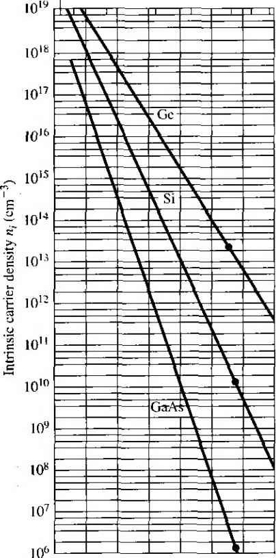 0.5 1.0 1.5 2.0 2.5 3.0 3.5 4.0 1000/ Figure 4.21 The intrinsic carrier concentration of Ge, Si, and GaAs as a function of temperature. (From Szeinj.) TEST YOUR UNDERSTANDING E4.3 Find the intrinsic carrier concentration in silicon at (й) Г = 200 К and (h) T = 400 K. E4.4 Repeat E4.3 for GaAs. [-шэ oi x SZ£ № Ч-шэ 2£ I Ф) -suy] E4.5 Repeat E4.3 for Ge. U- и01 x 9S (Ф oiO( x 9ГЗ W у] 4.1.4 The Intrinsic Fermi-Level Position We have qualitatively argued that the Fermi energy level is located near the center of the forbidden bandgap for the intrinsic semiconductor. We can specifically calculate the intrinsic Fermi-level position. Since the electron and hole concentrations are equal, setting Equations (4.20) and (4.21) equal to each other, we have Л^ехр - exp (4.24) If we take the natural log of both sides of this equation and solve for En, we obtain 1 1 /N, En = :(E,.E,) + -kT\n{- 2 2 \Nc (425) From the definitions for N,. and /У^, given by Equations (4.10) and (4.18), respectively. Equation (4.25) may be written as 1 3 , /m;\ (4.26ai The first term, (£ Ey), is the energy exacdy midway between and E. or the midgap energy. We can define SO that 3 ffnl\ Eh - Emidgap E\n j (4.26b If the electron and hole effective masses are equal so that m* = w*, then the intrin sic Fermi level is exactly in the center of the bandgap. If > ш*, the intrinsic Fermi level is slightly above the center, and if < it is slightly below the center of the bandgap. The density of states function is directly related to the carrier effective mass; thus a larger effective mass means a larger density of states funcfion, The intrinsic Fermi level must shift away from the band with the larger density of states in order to maintain equal numbers of electrons and holes. EXAMPLE 4.4 Objective To calculate the position of the intrinsic Fermi level with respect to the center of the bandgap in sihcon at r = 300 K. The density of states effective carrier masses in silicon are z = 1.08 ?u and m* 0.560. Solution The intrinsic Fermi level with respect to the center of the bandgap is 3 /К\ 3 , /0.56 Er - b.ia.ap = -kT In iJ = (0.0259) In Eli - E midgap = -0.0128 eV = 12.8 meV Comment The intrinsic Fermi level in silicon is 12.8 meV below the midgap energy. If we compare 12.8 meV to 560 meV, which is one-half of the bandgap energy of silicon, we can, in many applications, simply approximate the intrinsic Fermi level to be in the center of the bandgap. TEST YOUR UNDERSTANDING E4.6 Determine the position of the intrinsic Fermi level with respect to the center of the bandgap in GaAs at T = 300 K. (А^ш VSi- W) 4.2 I DOPANT ATOMS AND ENERGY LEVELS The intrinsic semiconductor may be an interesting material, but the real power of semiconductors is realized by adding small, controlled amounts of specific dopant, or impurity, atoms. This doping process, described briefly in Chapter 1, can greatly alter the electrical characteristics of the semiconductor. The doped semiconductor, called an extrinsic material, is the primary reason we can fabricate the various semiconductor devices that we will consider in later chapters. 4.2Л Qualitative Description In Chapter 3, we discussed the covalent bonding of silicon and considered the simple two-dimensional representation of the single-crystal silicon lattice as shown in Figure 4.3. Now consider adding a group V element, such as phosphorus, as a sub-sfitutionai impurity. The group V element has five valence electrons. Four of these will contribute to the covalent bonding with the silicon atoms, leaving the fifth more loosely bound to the phosphorus atom. This effect is schematically shown in Figure 4.4. We refer to the fifth valence electron as a donor electron. 11 11 ---- Si = Si -z Si = Si I = Si - Si - Si = = - Si = Si = Si 11 11 Si 11 11 11 Si = Si = Si Si = Si Si = Si --- Si - = -11 Figure 4.3 I Two-dimensional representation of the intrinsic silicon lattice. n II II Ii II 11 = Si ------ Si II I I 11 I r L I f I t1 \ I Si = Si = Si = Si - = - Si ------ Si --- Si ------ Figure 4.4 (Two-dimensional representation of the silicon lattice doped with a phosphorus atom. The phosphorus atom without the donor electron is positively charged. At very low temperatures, the donor electron is bound to the phosphorus atom. However by intuition, it should seem clear that the energy required to elevate the donor electron into the conduction band is considerably less than that for the electrons involved in the covalent bonding. Figure 4.5 shows the energy-band diagram that we would expect. The energy level, E, is the energy state of the donor electron. If a small amount of energy, such as thermal energy, is added to the donor elec tron, it can be elevated into the conduction band, leaving behind a positively charged phosphorus ion. The electron in the conduction band can now move through the crystal generating a current, while the positively charged ion is fixed in the crystal. This type of impurity atom donates an electron to the conduction band and so is called a donor impurity atom. The donor impurity -dtoms add electrons to the conduction band without creating holes in the valence band. The resulting material is referred to as an n-type semiconductor {n for the negatively charged electron). Now consider adding a group III element, such as boron, as a substitutional impurity to silicon. The group 111 element has three valence electrons, which are all taken up in the covalent bonding. As shown in Figure 4.6a, one covalent bonding position appears to be empty. If an electron were to occupy this empty position, its с с о Conduction band Valence barad (a) £. с с о ь Figure 4.5 t The energy-band diagram showing (a) the discrete donor energy state and (b) the effect of a donor state being ionized. --- Si --- Si --- Si --- Si II I Si --- Si ------ ------ Si Si -, В = Si --- = Si 11 i Si = Si --- 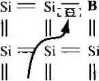 Si - - Si - Si - Si - Si - Si Figure 4.6 I Two-dimensional representation of a silicon lattice (a) doped with a boron atom and (b) showing the ionization of the boron atom resulting in a hole. i Conduction band DO £p I-------о Valence band + V + (a) (b) Figure 4.7 I The energy-band diagram showing (a) the discrete acceptor energy state and (b) the effect of an acceptor state being ionized. energy would have to be greater than that of the valence electrons, since the net charge state of the boron atom would now be negative. However, the electron occupying this empty position does not have sufficient energy to be in the conduction band, so its energy is far smaller than the conduction-band energy. Figure 4.6b shows how valence electrons may gain a small amount of thermal energy and move about in the ciystah The empty position associated with the boron atom becomes occupied, and other valence electron positions become vacated. These other vacated electron positions can be thought of as holes in the semiconductor material. Figure 4.7 shows the expected energy state of the empty position and also the formation of a hole in the valence band. The hole can move through the crystal generating a current, while the negatively charged boron atom is fixed in the crystal. The group 111 atom accepts an electron from the valence band and so is referred to as an acceptor impurity atom. The acceptor atom can generate holes in the valence band without generating electrons in the conduction band. This type of semiconductor material is referred to as a p-type material (p for the positively charged hole). The pure single-crystal semiconductor material is called an intrinsic material. Adding controlled amounts of dopant atoms, either donors or acceptors, creates a material called an extrinsic semiconductor. An extrinsic semiconductor will have either a preponderance of electrons (n type) or a preponderance of holes (p type). 4.2.2 Ionization Energy We can calculate the approximate distance of the donor electron from the donor impurity ion, and also the approximate energy required to elevate the donor electron into the conduction band. This energy is referred to as the ionization energy. We will use the Bohr model of the atom for these calculations. The justification for using this model is that the most probable distance of an electron from the nucleus in a hydrogen atom, determined from quantum mechanics, is the same as the Bohr radius. The energy levels in the hydrogen atom determined from quantum mechanics are also the same as obtained from the Bohr theory. In the case of the donor impurity atom, we may visualize the donor electron or-bifing the donor ion, which is embedded in the semiconductor material. We will need lo use the permittivity of the semiconductor material in the calculations rather than the pertnittivity of free space as is used in the case of the hydrogen atom. We will use the effective mass of the electron in the calculations. The analysis begins by setting the coulomb force of attraction between the el tron and ion equal to the centripetal force of the orbiting electron. This condition w give a steady orbit. We have 2 +2 e m V where v is the magnitude of the velocity and г is the radius of the orbit. If we assi the angular momentum is also quantized, then we can write mrv - nil (4.i where /7 is a positive integer. Solving for v from Equation (4.28), substituting ii; Equation (4.27), and solving for the radius, we obtain The assumption of the angular momentum being quantized leads to the radius being quanUzed. The Bohr radius is defined as 4jr6o ao = -V = 0-53 A (4J We can normalize the radius of the donor orbital to that of the Bohr radius, which giv . . . (4.3 where €r is the relative dielectric constant of the semiconductor material, mo is ti rest mass of an electron, and m is the conductivity effecrive mass of the electron the semiconductor. If we consider the lowest energy state in which n = \ , and if we consider silid in which = i\J and the conductivity effecrive mass is m*/mo = 0.26, then\ have that = 45 (4.; or r\ - 23.9A. This radius corresponds to approximately four lattice constants! silicon. Recall that one unit cell in silicon effectively contains eight atoms, so the i dius of the orbiting donor electron encompasses many silicon atoms. The donor ele tron is not rightly bound to the donor atom. The total energy of the orbiting electron is given by ET + V (4.: 1 ... 9 10 11 12 13 14 15 ... 55 |
|
© 2026 AutoElektrix.ru
Частичное копирование материалов разрешено при условии активной ссылки |