 |
 |
 |
| Главная Журналы Популярное Audi - почему их так назвали? Как появилась марка Bmw? Откуда появился Lexus? Достижения и устремления Mercedes-Benz Первые модели Chevrolet Электромобиль Nissan Leaf |
Главная » Журналы » Absorbing materialorganic polymer 1 ... 10 11 12 13 14 15 16 ... 55 where T is the kinetic energy and V is the potential energy of the electron. The kinetic energy is T -= m*v (4.34) Using the velocity v from Equation (4.28) and the radius r from Equation (4.29), the kinetic energy becomes ♦ T =---r (4.35) The potential energy is у - (4 36) 4яег, (nfi)2(47r€)2 The total energy is the sum of the kinetic and potential energies, so that £ = T + V -~--r (4.37) For the hydrogen atom, = mo and 6 6(>. The ionization energy of the hydrogen atom in the lowest energy state is then E - -13.6 eV. If we consider silicon, the ionization energy is E = -25.8 meV, much less than the bandgap energy of silicon. This energy is the approximate ionization energy of the donor atom, or the energy required to elevate the donor electron into the conduction band. For ordinary donor impurities such as phosphorus or arsenic in silicon or ger-manium, this hydrogenic model works quite well and gives some indication of the magnitudes of the ionization energies involved. Table 4.3 lists the actual experimentally measured ionization energies for a few impurities in silicon and germanium. Germanium and silicon have different relative dielectric constants and effective masses; thus we expect the ionization energies to differ. 4.2.3 Group lU-V Semiconductors In the previous sections, we have been discussing the donor and acceptor impurities in a group IV semiconductor, such as silicon. The situation in the group III-V Table 4.3 J Impurity ionization energies in silicon and germanium Ionization energy (eV)
compound semiconductors, such as gallium arsenide, is more complicated. Group elements, such as beryllium, zinc, and cadmium, can enter the lattice as subsr tional impurities, replacing the group 111 gallium element to become acceptor impu-riries. Similarly, group VI eleinents, such as selenium and tellurium, can enter ihe lattice substitutionally, replacing the group V arsenic element to become donor impurities. The corresponding ionization energies for these impurities are smaller than for the impurities in silicon. The ionization energies for the donors in gallium arsenide are also smaller than the ionization energies for the acceptors, because of the smaller effective mass of the electron compared to that of the hole. Group IV elements, such as silicon and gennanium, can also be impurity atoms in gallium arsenide. If a silicon atom replaces a gallium atom, the silicon impurity will act as a donor, but if the silicon atom replaces an arsenic atom, then the silicon impurity will act as an acceptor. The same is true for germanium as an impurity atom. Such impurities are called amphoteric. Experimentally in gallium arsenide, it is found that germanium is predominantly an acceptor and silicon is predominantly a donor. Table 4.4 lists the ionization energies for the various impurity atoms in gallium arsenide. TEST YOUR UNDERSTANDING E4.7 Calculate the radius (normalized to a Bohr radius) of a donor electron in its lowest energy state in GaAs. (£561 suy) 4.3 I THE EXTRINSIC SEMICONDUCTOR We defined an intrinsic semiconductor as a material with no impurity atoms pres in the crystal. An extrinsic semiconductor is defined as a semiconductor in whi controlled amounts of specific dopant or impurity atoms have been added so that thermal-equilibrium electron and hole concentrations are different from the intrii 4-3 The Exth nsic Sem iconductor carrier concentration. One type of carrier will predominate in an extrinsic semiconductor. 4.3.1 Equilibrium Distribution of Electrons and Holes Adding donor or acceptor impurity atoms to a semiconductor will change the distribution of electrons and holes in the material. Since the Fermi energy is related to the distribution function, the Fermi energy will change as dopant atoms are added. If the Femii energy changes from near the midgap value, the density of electrons in the conduction band and the density of holes in the valence band will change. These effects aie shown in Figures 4.8 and 4.9. Figure 4.8 shows the case for Et > Efi and Figure 4.9 shows the case for < E,. When Ef > Efi, the electron concentration is larger than the hole concentration, and when E < Efi, the hole concentration 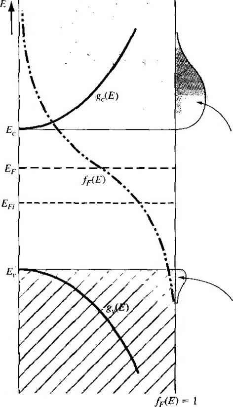 Area = - electron concentration Area = pQ = hole concentration fr(E) = 0 Figure 4.81 Density of states functions, Fermi-Dirac probability function, and areas representing electron and hole concentrations for the case when Ef is above the intrinsic Fermi energy. 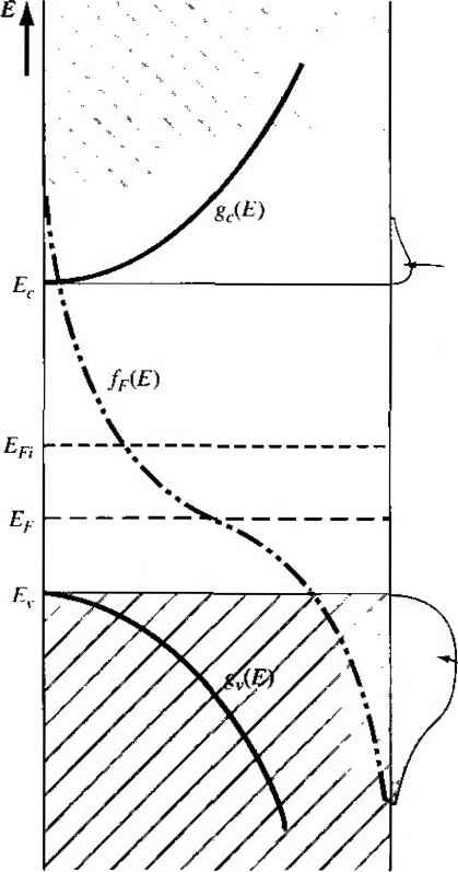 Area = rtf, electron concentration Area = = hole concentration friE) = 1 Figure 4.9 1 Density of states functions, Fermi-Dirac probability function, and areas representing electron and hole concentrations for the case when Ej. is below the intrinsic Fermi energy. is larger than the electron concentration. When the density of electrons is greater than the density of holes, the semiconductor is n type; donor impurity atoms have been added. When the density of holes is greater than the density of electrons, the semiconductor is p type; acceptor impurity atoms have been added. The Fermi energy level in a semiconductor changes as the electron and hole concentrations change and, again, the Fermi energy changes as donor or acceptor impurities are added. The change in the Fermi level as a function of impurity concentrations will be considerecy in Section 4.6. The expressions previously derived for the thermal-equilibrium concentrarion electrons and holes, given by Equations (4.11) and (4.19) are general equations for HQ and Po in terms of the Fermi energy. These equations are again given as По = exp (E, - Er) кТ 4.3 The Extrinsfc Semiconductor Po - N exp As we just discussed, the Fermi energy may vary through the bandgap energy, which will then change the values of о and po. Objective To calculate the thermal equilibrium concentrations of electrons and holes for a given Fermi energy. Consider silicon at Г = 300 К so that N, = 2.8 x 10 cm and N, = 1.04 x 10 cm. Assume thai Ihe Fermi energy is 0.25 eV below the conduction band. If we assume that the bandgap energy of silicon is 1.12 eV, then the Fermi energy will be 0.87 cV above the valence band. Solution Using Equation (4.11), we have j 0 = (2-8 X I0)exp (5) = Ь8 x lO cm From Equation (4.19), we can write Po = (1.04 X lOexp = 2Л x 10 cm Comment The change in the Fermi level is actually a function of the donor or acceptor impurity conccn-Uations that are added to the semiconductor However, this example shows that electron and hole concentrations change by orders of magnitude from the intrinsic carrier concentration as the Fermi energy changes by a few tenths of an electron-volt. EXAMPLE 4.5 In this example, since o > Po. the semiconductor is n type. In an n-type .semiconductor, electrons are referred to as the majority carrier and holes as the minority carrier. By comparing the relative values of о and po in the example, it is easy to see how this designation came about. Similarly, in a p-type semiconductor where po > 0, holes are the majority carrier and electrons are the minority carrier. We may derive another form of the equations for the thermal-equilibrium concentrations of electrons and holes. If we add and subtract an intrinsic Fermi energy in the exponent of Equation (4.11), we can write no = Nc exp (E,.-En){ErE,i) (4.38a) no - Л^г exp (E, - En) kT (Er - Efi) kT (4.38b) The intrinsic carrier concentration is given by Equation (4.20) as Л, = N exp -(E, - En) кТ so that the thermal-equilibrium electron concentration can be written as nt = m exp Ef - Efi кТ (4.39) Similarly, if we add and subtract an intrinsic Fermi energy in the exponent of Eqi tion (4.19), we will obtain Po = щ exp -JEf - En) кТ (4.40) As we will see, the Fermi level changes when donors and acceptors are added, but Equations (4.39) and (4.40) show that, as the Fermi level changes from the intrinsic Fermi level, fiq and po change from the /г,- value. If Ef > Efi, then we will have по> rij and Po < One characteristic of an n~t у pe semiconductor is that > Efi so that л0 > Po- Similarly, in a p-type semiconductor, Ef < En so that po > , ai щ < tt,; thus/?o > 0- We can see the functional dependence of no and po with Ef in Figures 4.8 and 4.9. As £f moves above or below Efj, the overlapping probability function with the density of states functions in the conduction band and valence band changes. As Ef moves above Efi, the probability funcrion in the conduction band increases, while the probability, 1 - ffiE), of an empty state (hole) in the valence band decreases. As Ef moves below Efi, the opposite occurs. 4.3-2 The rto po Product We may take the product of the general expressions for no and po as given in Equations (4.11) and (4.19), respectively. The result is noPo - NcN exp -(E,-Ef) кТ -{Ef - E,) кТ (4.41) which mav be written as oPo = cv exp (4.42) As Equarion (4.42) was derived for a general value of Fermi energy, the values of rto and Po are not necessarily equal. However, Equation (4.42) is exactly the same as Equation (4.23), which we derived for the case of an intrinsic semiconductor We 4-3 The Extrinsic Semicond uctor then have that, for the semiconductor in thermal equilibrium, nopo =п^ (443) Equation (4.43) states that the product of no and p is always a constant for a given semiconductor material at a given temperature. Although this equation seems very simple, it is one of the fundamental principles of semiconductors in thermal equiHbrium. The significance of this relation will become more apparent in the chapters that follow. It is important to keep in mind that Equation (4.43) was derived using the Boltzmann approximation. If the Boltzmann approximation is not valid, then likewise. Equation (4.43) is not valid. An extrinsic semiconductor in thermal equilibrium does not, strictly speaking, contain an intrinsic carrier concentration, although some thermally generated carriers are present. The intrinsic electron and hole carrier concentrations are modified by the donor or acceptor impurities. However, we may think of the intrinsic concentration tii in Equation (4.43) simply as a parameter of the semiconductor material. ♦4ДЗ The Fermi-Dirac Integral In the derivation of the Equations (4Л1) and (4Л 9) for the thermal equilibrium electron and hole concentrations, we assumed that die Boltzmann approximation was valid. If the Boltzmann approximation does not hold, the thermal equilibrium electron concentration is written from Equation (4.3) as no = -(2m r-oc 1 -h exp E-E, kT If we again make a change of variable and let E-E, and also define Ef - Ec kT then we can rewrite Equation (4.44) as \ J Jo i-\-txp(r]-i]f) (4.44) (4.45a) (4.45b) (4.46) The integral is defined as Eifiinr) = / 1 +exp(/ - Y]f) (447) .5 10 -6 -4 -2 0 2 - £,) :T - щ Figure 4Л0 I The Fermi-Dirac integral F]/2 as a function of the Fermi energy. {From Sze 113j,} This function, called the Fermi-Dirac integral, is a tabulated function of the variabl r]f. Figure 4Л0 is a plot of the Fermi-Dirac integral. Note that if r}f > 0, the Ef > Ec \ thus the Fermi energy is actually in the conduction band. EXAMPLE 4.6 Objective To calculate the electron concentration using the Fermi-Dirac integral. Let rjf =2 so that the Fermi energy is above the conduction band by approximate! 52 meV at Г = 300 К. Solution Equation (4.46) can be written as .Е^а(пг) For silicon at 300 K, Af = 2.8 x 10* cm and, from Figure 4.10, the Fermi-Dirac ititegrs has a value of /1/2(2) =2.3, Then fto = (2.8 X 10)(2.3) = 7.27 x 10 cm 4.3 The Extrinsic 8еглiconductor 127 Comment Note that if we had used Equation (4.11), the thermal equilibrium value of пи would be По = 2.08 X 10- cm~, which is incorrect since the Boltzmann approximation is not valid for this case. We may use the same general method to calculate the thermal equilibrium concentration of holes. We obtain p==4n{) / (4.48) / /о 1+exp(7]- where  n = (4,49a) * Eli - Ep ki The integral in Equation (4.48) is the same Fermi-Dirac integral defined by Equation (4.47), although the variables have slightly different definitions. We may note that if rjjr > 0, then the Fermi level is in the valence band. TEST YOUR UNDERSTANDING E4-8 Calculate the thermal equilibrium electron concentration in silicon for the case when Ef = E, and T = 300 K. (- 6iOl x 6 I V) 4.3.4 Degenerate and Nondegenerate Semiconductors In our discussion of adding dopant atoms to a semiconductor, we have implicitly assumed that the concentration of dopant atoms added is small when compared to the density of host or semiconductor atoms. The small number of impurity atoms are spread far enough apart so that there is no interacrion between donor electrons, for example, in an n-type material. We have assumed that the impurities introduce discrete, noninteracting donor energy states in the n-type semiconductor and discrete, noninteracfing acceptor states in the p-type semiconductor. These types of semiconductors are referred to as nondegenerate semiconductors. If the impurity concentration increases, the distance between the impurity atoms decreases and a point will be reached when donor electrons, for example, will begin to interact with each other. When this occurs, the single discrete donor energy will split into a band of energies. As the donor concentration further increases, the band of donor states widens and may overlap the bottom of the conduction band. This overiap occurs when the donor concentration becomes comparable with the effective density of states. When the concentration of electrons in the conduction band exceeds Conduction band с и Conduction band JJl...,MJ Filled states (electrons) Venceband Empty states (holes) .- . - .ЧЯ jj-i Valence band Figure 4Л1 Simplified energy-band diagrams for degenerately doped (a) n-type and (b) Ptype semiconductors. the density of states Л/., the Fermi energy Ues within the conduction band. Thisty of semiconductor is called a degenerate n-type semiconductor. In a similar way, as the acceptor doping concentration increases in a p-typ semiconductor, the discrete acceptor energy states will split into a band of energie and may overlap the top of the valence band. The Fermi energy will lie in the valetw band when the concentration of holes exceeds the density of states jV - This type о semiconductor is called a degenerate p-type semiconductor. Schematic models of the energy-band diagrams for a degenerate n-type and de generate p-type semiconductor are shown in Figure 4.11. The energy states below £ are mostly filled with electrons and the energy states above Ef are mostly empty, the degenerate n-type semiconductor, the states between Ef and E are mostly filh with electrons; thus, the electron concentration in the conduction band is very larg( Similarly, in the degenerate p-type semiconductor, the energy states between Ej, at) Ef are mostly empty; thus, the hole concentration in the valence band is very large 4.4 I STATISTICS OF DONORS AND ACCEPTORS In the last chapter, we discussed the Fermi-Dirac distribution function, which giv< the probability that a particular energy state will be occupied by an electron. We to reconsider this function and apply the probability statistics to the donor and acceptor energy states. give! 4.4.1 Probability Function One postulate used in the derivation of the Fermi-Dirac probability function was ihe Pauli exclusion principle, which states that only one particle is permitted in quantum state. The Pauli exclusion principle also applies to the donor and accept states. Suppose we have Л^, electrons and gj quantum states, where the subscript / indicates the iih energy level. There are g, ways of choosing where to put the first panicle. Each donor level has two possible spin orientations for the donor electron; th each donor level has two quantum states. The insertion of an electron into one q tum state, however, precludes putting an electron into the second quantum state  1 ... 10 11 12 13 14 15 16 ... 55 |
||||||||||||||||||||||||||||||||||||||||||||||||||||||||||||||||||||||||||||||||||||||||||||||||||||||||||||||||||||||||||||||||||||||||||||||||||||||||||||||||||||||||||||||||||||||||||||||||||||||||||||||||||||||||||||||||||||||||||||||||||||||||||||||||||||||||||||||||||||||||||||||||||||||||||||||||||
|
© 2026 AutoElektrix.ru
Частичное копирование материалов разрешено при условии активной ссылки |