 |
 |
 |
| Главная Журналы Популярное Audi - почему их так назвали? Как появилась марка Bmw? Откуда появился Lexus? Достижения и устремления Mercedes-Benz Первые модели Chevrolet Электромобиль Nissan Leaf |
Главная » Журналы » Absorbing materialorganic polymer 1 ... 11 12 13 14 15 16 17 ... 55 adding one electron, the vacancy requirement of the atom is satisfied, and the addition of a second electron in the donor level is not possible. The distribution function of donor electrons in the donor energy states is then slightly different than the Fermi-Dirac function. The probability function of electrons occupying the donor state is =-;--- (4.50) 1 (E,-Er\ where nj h the density of electrons occupying the donor level and Ej is the energy of the donor level. The factor 5 in this equation is a direct result of the spin factor just mentioned. The \ factor is sometimes written as 1/g, where g is called a degeneracy factor. Equation (4.50) can also be written in the form ridN-N (4.51) where is the concentration of ionized donors. In many applications, we wtU be interested more in the concentration of ionized donors than in the concentration of electrons remaining in the donor states. If we do the same type of analysis for acceptor atoms, we obtain the expression A.---vV - (4-52) where Л^ s the concentration of acceptor atoms, is the acceptor energy level, р„ is the concentration of holes in the acceptor states, and Af7 is the concentration of ionized acceptors. A hole in an acceptor state corresponds to an acceptor atom that is neutrally charged and still has an empty bonding position as we discussed in Section 4.2.1. The parameter g is, again, a degeneracy factor. The ground state degeneracy factor g is normally taken as four for the acceptor level in silicon and gallium arsenide because of the detailed band structure. 4.4.2 Complete Ionization and Freeze-Out The probability function for electrons in the donor energy state was just given by Equation (4.50). If we assume that (E - Ef) kT, then -j-77--- ld exp . I (E, ~ ЕЛ -(Ed - Ef) kT (4.53) If {Ej - Ej.) kT, then the Boltzmann approximation is also valid for the electrons in the conduction band so that, from Equation (4.11), 0 = N(: exp  EXAMPLE 4.7 We can determine the relative number of electrons in the donor state compa with the total number of electrons; therefore we can consider the ratio of electrom the donor state to the total number of electrons in the conduction band plus doi state. Using the expressions of Equations (4.53) and (4.11), we write
(4,! The Fermi energy cancels out of this expression. Dividing by the numerator term, obtain rid + no , , к 2Nr} -JEc - Ed) кТ (4.5 The factor (£ Ed) is just the ionization energy of the donor electrons. Objective To determine the fraction of total electrons still in the donor states at Г = 300 K. Consider phosphorus doping in silicon, for T 300 K, at a concentration of lO cm- Solution Using Equation (4.55), we find 0 +fd , 2.8x10 /-0.045 \ 1 -I-- ,7- exp = 0.0041 =0.41% 2(10) 0.0259 Ш ComnDent This example shows that there are very few electrons in the donor state compared with th conduction band. Essentially all of the electrons from the donor states are in the conductio band and, since only about 0.4 percent of the donor states contain electrons, the donor state are said to be completely ionized. At room temperature, then, the donor states are essentially completely ionize* and, for a typical doping of 10 cm~\ almost all donor impurity atoms have donatet an electron to the conduction band. At room temperature, there is also essentially complete ionization of the acceptor atoms. This means that each acceptor atom has accepted an electron from the valence band so that Pa is zero. At typical acceptor doping concentrations, a hole is ere ated in the valence band for each acceptor atom. This ionization effect and the creation of electrons and holes in the conduction band and valence band, respectively, are shown in Figure 4.12. Conduction band Conduction band ) ) ) ) ) ) ) + + + + + + + ~ E. Valence band - + + + + + + Valence band , i Figure 4Л2 1 Energy-band diagrams showing complete ionization of (a) donor states and (b) acceptor states. Conduction band Conduction band E С Ш Valence band (a) с с  fValencc band Figure 4.13 I Energy-band diagram at Г = 0 К for (a) n-type and (b) p-type semiconductors. The opposite of complete ionization occurs at 7 = 0 K. At absolute zero degrees, all electrons are in their lowest possible energy state; that is, for an n-type semiconductor, each donor state must contain an electron, therefore n,i - or JV+ = 0. We must have, then, from Equation (4.50) that exp \ {Е^ - E)/kT] - Q. Since Г = 0 K, this will occur for exp (-oo) =0, which means that Ef > Ej. The Fermi energy level must be above the donor energy level al absolute zero. In the case of a p-type semiconductor at absolute zero temperature, the impurity atoms will not contain any electrons, so that the Fermi energy level must be below the acceptor energy state. The distribution of electrons among the various energy states, and hence the Fermi energy, is a function of temperature. A detailed analysis, not given in this text, shows that at Г - 0 K, the Fermi energy is halfway between and Ej for the n-type material and halfway between E and Ev for the p-lype material. Figure 4.13 shows these effects. No electrons from the donor state are thermally elevated into the conduction band; this effect is called freeze-out. Similarly, when no electrons from the valance band are elevated into the acceptor states, the effect is also called freeze-out. EXAMPLE 4.8 Between T = 0 K, freeze-out, and T = 300 K, complete ionization, we hav( partial ionization of donor or acceptor atoms. Objective To detenmine the temperature at which 90 percent of acceptor atoms are ionized. Consider p-type silicon doped with boron at a concentration of N - 10 cm~. Solution Find the ratio of holes in the acceptor state to the total number of holes in the valence band pit acceptor state. Taking into account the Boltzmann approximation and assuming the degenerj асу factor is g = 4, we write Pi) + Pa I , 1 + exp 4JV. {Eg - £.) кТ For 90 percent ionization. Po + pa = 0.10 = (L04 X 10**) 1 -h 4(101*) exp -0.045 0.0259 (зоо) LJsing trial and error, we find that T = 193 K. Comment This example shows that at approximately 100 С below room temperature, we sfill hav 90 percent of the acceptor atoms ionized; in other words, 90 percent of the acceptor atoms have donated a hole to the valence band. TEST YOUR UNDERSTANDING E4,9 Determine the fraction of total holes still in the acceptor states in silicon at Г = 300 К for a boron impurity concentration of N. = 10 cm~-. (б^ГО ny) E4.10 Consider sihcon with a phosphorus impurity concentration of Л^, = 5 x 10 cm l Plot the percent ot ionized impurity atoms versus temperature over ihe range 100 < T < 400 K. 4.5 I CHARGE NEUTRALITY In thermal equilibrium, the semiconductor crystal is electrically neutral. The el( Irons are distributed among the various energy states, creating negative and positii charges, but the net charge density is zero. This charge-neutrality condition is used determine the thermal-equilibrium electron and hole concentrations as a function the impurity doping concentration. We will define a compensated semiconductor and then determine the electron and hole concentrations as a function of the donor and acceptor concentrations. 4.5.1 Compensated Semiconductors A compensated semiconductor is one that contains both donor and acceptor impurity atoms in the same region. A compensated semiconductor can be formed, for example, by diffusing acceptor impurities into an n-type material, or by diffusing donor impurities into a p-type material. An n-type compensated semiconductor occurs when > Na, and a p-type compensated semiconductor occurs when Na > N IfNa = we have a completely compensated semiconductor that has, as we will show, the characteristics of an intrinsic material. Compensated semiconductors are created quite naturally during device fabrication as we will see later. 4.5.2 Equilibrium Electron and Hole Concentrations Figure 4.14 shows the energy-band diagram of a semiconductor when both donor and acceptor impurity atoms are added to the same region to form a compensated Thermal electrons Total electron concentration Donor electrons Un-ionized donors If * Ionized donors Un-ionized acceptors - (K. - Pa) Ionized acceptors - E.
Thermal holes V ;..... Po ( Total hole concentration Acceptor holes Figure 4.14 I Energy-band diagram of a compensated semiconductor showing ionized and un-ionized donors and acceptors. semiconductor. The figure shows how the electrons and holes can be distribute among the various states. j The charge neutrality condition is expressed by equating the density of negativd charges to the density of positive charges. We then have щ + Л^- = Po + (4.56 0 + (K, - Po) = Po-\~(Nci - rtrf) (4.5 where о and pQ are the thermal-equilibrium concentrations of electrons and holes i the conduction band and valence band, respectively. The parameter n, is the сопсея tration of electrons in the donor energy states, so = Nd - п,{ is the concentratiol of positively charged donor states. Similarly, Pa is the concentration of holes in thj acceptor states, so N~ = N - Pa is the concentration of negatively charged acceptor states. We have expressions for no, pQn, and p in terms of the Fermi energy and temperature. If we assume complete ionization, n and Pa are both zero, and Equarion (4.57) becomes J 0 + К Po + j (4.58) If we express po as nj/пц, then Equation (4.58) can be written as 0 + = - + Nd (4.59a) which in turn can be written as nl - (Nj - Na)no -nj=0 (4.59b) The electron concentration no can be determined using the quadratic formula, or 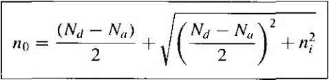 (4.60) The positive sign in the quadratic formula must be used, since, in the limit of an intrinsic semiconductor when N. = = 0, the electron concentration must be a positive quantity, or По = п/ Equation (4.60) is used to calculate the electron concentration in an n-type semiconductor, or when Nd > Na- Although Equation (4.60) was derived for a compensated semiconductor, the equation is also valid for N = 0. EXAMPLE 4.9 Objecdvc To determine the thermal equilibrium electron and hole concentrations for a given doping concentration. Consider an n-type silicon semiconductor at T = 300 К in which = 10 cm and =0. The intrinsic carrier concentration is assumed to be = 1.5 x 10 cm~. Solution From Equation (4.60), the majority carrier electron concentration is no = 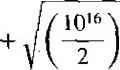 + (L5 X 10*) = 10* cm The minority carrier hole concentration is found as nj (LSxlOif) 1 X 10f> - 2.25 X 10 cm Comment In this example, iVj > , so that the thermal-equilibrium majority carrier electron concentration is essentially equal to the donor impurity concentration. The thermal-equilibrium majority and minority carrier concentrations can differ by many orders of magnitude. We have argued in our discussion and we may note from the results of Example 4.9 that the concentration of electrons in the conduction band increases above the intrinsic carrier concentration as we add donor impurity atoms. At the same time, the minority carrier hole concentration decreases below the intrinsic carrier concentration as we add donor atoms. We must keep in mind that as we add donor impurity atoms and the corresponding donor electrons, there is a redistribution of electrons among available energy states. Figure 4Л5 shows a schematic of this physical redistribution. A few of the donor electrons will fail into the empty states in the valence Intrinsic electrons ♦ )))))) + + + + + + Ionized donors Un-ionized donors Л few donor electrons annihilate some mtnnsic holes ©0© У Intrinsic holes Netpo- Figure 4Л5 1 Energy-band diagram showing the redistribution of electron.s when donors are added. EXAMPLE 4.10 Objective To calculate the thermal-equilibrium electron and hole concentrations in a germanium sample for a given doping density. Consider a germanium sample at Г = 300 К in which - 5 x lO cm * and = Assume that tt, 2.4 x 10* cm~*. Solution Again, from Equation (4.60), the majority carrier electron concentration is 5X10 [TsZioY . n . 0 = -+ JI-~ j + (2.4 X 10) = 5 .97 X 10 cm The minority carrier hole concentration is nj (2.4 X 10-) P(, = = -= 9.65 X 10 cm-- no 5.97 X 10 Ш Comment If the donor impurity concentration is not too different in magnitude from the intrinsic carrier concentration, then the thermal-equilibrium majority carrier electron concentration is influenced by the intrinsic concentration. We have seen that the intrinsic carrier concentration ni is a very strong function of temperature. As the temperature increases, additional electron-hole pairs are thermally generated so that the nj term in Equation (4.60) may begin to dominate. The semiconductor will eventually lose its extrinsic characteristics. Figure 4.16 shows the electron concentration versus temperature in silicon doped with 5 x 10 * donors per cm. As the temperature increases, we can see where the intrinsic concentration begins to dominate. Also shown is the partial ionizarion, or the onset of freeze-out, at the low temperature. If we reconsider Equation (4.58) and express о as n/po, then we have L+N =po + N (4.61a which we can write as Po - -Nj)pQ-nj=0 (4.611 band and, in doing so, will annihilate some of the intrinsic holes. The minority carrier hole concentration will therefore decrease as we have seen in Example 4.9, At the same rime, because of this redistribution, the net electron concentration in the conducrion band is not simply equal to the donor concentration plus the шгщ electron concentration. £ Intrinsic. Extrinsic Partial ionization  100 200 300 400 500 600 700 T(K) Figure 4.16 I Electron concentration versus temperature showing the three regions: partial ionization, extrinsic, and intrinsic. Using the quadratic formula, the hole concentration is given by 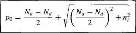 (4-62) where the positive sign, again, must be used. Equation (4.62) is used to calculate the thermal-equilibrium majority carrier hole concentration in a p-type semiconductor, or when Na > Ntj. This equation also applies for /V = 0. Objective To calculate the thermal-equilibrium electron and hole concentrations in a compensated p-iype semiconductor. Consider a silicon semiconductor at 7 = 300 К in which N = \0 cm~ and Nj = 3x lO- cm~-\ Assumertг = 1.5 x 10 cm -. Solution Since Na > N, the compensated semiconductor is p-type and the thermal-equilibrium majority carrier hole concentration is given by Equation (4.62) as so that Po =--+J(- j +(1.5x10 ) EXAMPLE 4.11 15 -3 Pi)7 X 10 cm 3:21 X 10 cm Comment If we assume complete ionization and if (iVa - N) j, then the majority carrier hole coi centration is, to a very good approximation, just the difference between the acceptor and donfl concentrations. We may note that, for a compensated p-type semiconductor, the minority cdnie electron concentrarion is determined from 0 = - = PO (K - Nd) DESIGN I Objective EXAMPLE 4.12  To determine the required impurity doping concentration in a semiconductor material. A silicon device with n-type material is to be operated at Г = 550 К. At this temperati the intrinsic carrier concentration must contribute no more than 5 percent of the total elect concentration. Determine the minimum donor concentration required to meet this specificati* Solution At Г = 550 K, the intrinsic carrier concentration is found from Equation (4.23) as nj = N,N,. exp (] = (2.8 x 10(1-04 x lO) (-V exp f f -V \кТ/ ЧЗООУ * [0.0259 V 550/, nr = 1.02 X 10 so that m =3.20x 10 cm For the intrinsic carrier concentration to contribute no more than 5 percent of the total electi concentration, we set о 1.05?Vj. From Equation (4.60), we have The minority carrier electron concentration is nj (L5 X 10 ) 1 ... 11 12 13 14 15 16 17 ... 55 |
||||||||||||||||
|
© 2026 AutoElektrix.ru
Частичное копирование материалов разрешено при условии активной ссылки |