 |
 |
 |
| Главная Журналы Популярное Audi - почему их так назвали? Как появилась марка Bmw? Откуда появился Lexus? Достижения и устремления Mercedes-Benz Первые модели Chevrolet Электромобиль Nissan Leaf |
Главная » Журналы » Absorbing materialorganic polymer 1 ... 12 13 14 15 16 17 18 ... 55  4 6 Position of Fermi Energy LeveJ which yields Ki L39 X 10-* cm Comment If the temperature remains less than 7 = 550 K, then the intrinsic carrier concentration will contribute less than 5 percent of the total electron concentration for this donor impurity concentration. Equations (4.60) and (4.62) are used to calculate the majority carrier electron concentration in an n-type semiconductor and majority carrier hole concentration in a p4ype semiconductor, respectively. The minority carrier hole concentration in an n-type semiconductor could, theoretically, be calculated from Equation (4.62). How- ever, we would be subtracting two numbers on the order of 10 cmfor example, to obtain a number on the order of 10 cm , which from a pracrical point of view is not possible. The minority carrier concentrations are calculated from nopQ the majority carrier concentration has been determined. fit once TEST YOUR UNDERSTANDING E4.11 Consider a compensated GaAs semiconductor at T 300 К doped at - 5 X iO cm and N = 2 x 10 cm \ Calculate the thermal equilibrium electron and hole concentrations. r-Ol 91T = i \- 9i01 1 = suy) Е4Л2 Silicon is doped atN= 10 cm and Л^ = 0. {a) Plot the concentration of electrons versus temperature over the range 300 T < 600 K. (b) Calculate the temperature at which the electron concentration is equal to LI x 10 cm~ \ iZl SUV) I POSITION OF FERMI ENERGY LEVEL We discussed qualitatively in Section 4.3.1 how the electron and hole concentrarions change as the Fermi energy level moves through the bandgap energy. Then, in Section 4.5, we calculated the electron and hole concentrations as a function of donor and acceptor impurity concentrations. We can now determine the position of the Fermi energy level as a function of the doping concentrations and as a function of temperature. The relevance of the Fermi energy level will be further discussed after the mathematical derivations. 4.6Д Mathematical Derivation The position of the Fermi energy level within the bandgap can be determined by using the equations already developed for the thermal-equilibrium electron and hole concentrations. If we assume the Boltzmann approximation to be valid, then from Equation (4.П) we have o - /V,. exp [-(Ec - Ef)/kT].We can solve for Ec - Ef from this equation and obtain 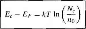 where no is given by Equation (4.60). If we consider an n-type semiconductor ii which Nd ni, then no N,[y so that E, = kT .n (I) (4.64) The distance between the bottom of the conduction band and the Fermi enersv is a logarithmic function of the donor concentration. As the donor concentration increases, the Fermi level moves closer to the conduction band. Conversely, if the Fermi level moves closer to the conduction band, then the electron concentrarion in the conduction band is increasing. We may note that if we have a compensated semiconductor, then the term in Equation (4.64) is siinply replaced by Nj - Na, or the net effective donor concentration. DESIGN EXAMPLE 4.13  Objective To deteimine the required donor impurity concentration to obtain a specified Fermi energy. Silicon at 7 = 300 К contains an acceptor impurity concentration of Л^, = 10 cm \ Determine the concentration of donor impurity atoms that must be added so that the silicon is n type and the Fermi energy is 0.20 eV below the conduction band edge. Solution From Equation (4.64), we have E, - Er = kT In \n,-nJ which can be rewritten as Nd - N = N.. exp Then Nd -N, =2.8 X 10 exp ~-0.20 0.0259 = 1.24 X 10 cm- Nd = 1.24 X 10 -ЬЫ= 2.24 x 10 cm 16 -3 Comment A compensated semiconductor can be fabricated to provide a .specific Fermi energy level. 4.6 Position of Fermi Energy Level We may develop a slightly different expression for the position of the Fermi level. We had from Equation (4.39) that = п[ ехр1(£г - Efi)/kT]. We can solve for Ef - Efi as (4.65) 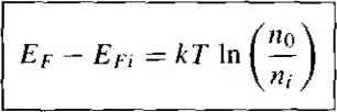 Equation (4.65) can be used specifically for an n-type semiconductor, where o is given by Equation (4.60), to find the difference between the Fermi level and the intrinsic Fermi level as a function of the donor concentration. We may note that, if the net effective donor concentration is zero, that is, - = 0, then no ni and Ef = Efi. A completely compensated semiconductor has the characteristics of an intrinsic material in terms of carrier concentration and Fermi level position. We can derive the same types of equations for a p-type semiconductor. From Equation (4.19), we have po =- N, exp {-(Ef - Е^,)/кТ] so that Ef - £r - kT In (4.66) If we assume that Л^ then Equation (4.66) can be written as Ef - Ег, - кТ In  (4.67) The distance between the Fermi level and the top of the valence-band energy for a p-type semiconductor is a logarithmic function of the acceptor concentration: as the acceptor concentration increases, the Fermi level moves closer to the valence band. Equation (4.67) still assumes that the Boltzmann approximation is valid. Again, if we have a compensated p-type semiconductor, then the Na term in Equation (4.67) is replaced by Na - Nti. or the net effective acceptor concentrarion. We can also derive an expression for the relationship between the Fermi level and the intrinsic Fermi level in terms of the hole concentrarion. We have from Equation (4.40) that Po ni exp [-(Ef - En)/kT], which yields (4.68) 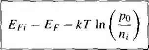 Equation (4.68) can be used to find the difference between the intrinsic Fermi level and the Fermi energy in terms of the acceptor concentration. The hole concentration Po in Equation (4.68) is given by Equation (4.62). We may again note from Equation (4.65) that, for an n-type semiconductor, 0 > rt/ and Ef > Efi. The Fermi level for an n-type semiconductor is above Efi. For a p-type semiconductor, po > <itid from Equation (4.68) we see that - £ Figure 4.17 I Position of Fermi level for an (a) n-type {N > and (b) p-type {N > NJ semiconductor Efi > Ef. The Fermi level for a p-type semiconductor is below Efi. These results are shown in Figure 4.17. 4.6.2 Variation of Ep with Doping Concentration and Temperature We may plot the position of the Fermi energy level as a function of the doping concentration. Figure 4.18 shows the Fermi energy level as a function of donor concentration (n type) and as a function of acceptor concentration (p type) for silicon T = 300 K. As the doping levels increase, the Fermi energy level moves closer to tl conduction band for the n-type material and closer to the valence band for the p-tyi material. Keep in mind that the equations for the Fermi energy level that we have rived assume that the Boltzmann approximation is valid. Nd (cm--) 10 -I- n type ptype 102 103 10 lO- 10 10 10* N, (cm-) Figure 4.18 I Position of Fermi level as a function of donor concentration (n type) and acceptor concentration (p type). Objective To determine the Fermi-level position and the maximum doping at which the Boltzmann approximation is stilt valid. Consider p-type silicon, at Г 300 K, doped with boron. We may assume that the limit of the Boltzmann approximation occurs when Ef - ЪкТ. (See Section 4.1.2.) Solution From Table 43, we find the ionizafion energy is - E. = 0,045 eV for boron in silicon. If we assume that Ец £midgap> then from Equafion (4.68), the position of the Fermi level at the maximum doping is given by EFi-Ef (E - E,) - (E, - E. 0.56 - 0.045 - 3(0.0259) = 0.437 = (0.0259) In  We can then solve for the doping as N = m exp 0.437 \ ,0.0259/ = 3.2 X 10 cm-- Comment If the acceptor (or donor) concentration in silicon is greater than approximately 3 x 10 cm , then the Boltzmann approximation of the distribution function becomes less valid and the equations for the Fermi-level position are no longer quite as accurate. EXAMPLE 4Л4 TEST YOUR UNDERSTANDING E4.13 Determine the position of the Fermi (eve! with respect to the valence band energy in p type GaAs at Г= 300 К. The doping concentrations are л/ 5 x 10 cm and Nj 4 X 10- cm- (A 0£Г0 = З - э suy) Е4Л4 Calculate the position of the Fermi energy level in n-type silicon at Г = 300 К with respect to the intrinsic Fermi energy level. The doping concentrations are = 2 x 10 cm- and N = 3 x 10 cm . (A9 1317-0 Э -SUV) The intrinsic carrier concentration /i, in Equations (4.65) and (4.68), is a strong function of temperature, so that Ef \s г function of temperature also. Figure 4.19 shows the variation of the Fermi energy level in silicon with temperature for several donor and acceptor concentrations. As the temperature increases, tii increases, and Ef moves closer to the intrinsic Fermi level. At high temperature, the semiconductor material begins to lose its extrinsic characteristics and begins to behave more like an intrinsic semiconductor. At the very low temperature, freeze-out occurs; the Boltzmann approximation is no longer valid and the equations we derived for the
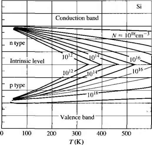 Figure 4.191 Position of Fermi level as a function of temperature for various doping concentrations. (From Sze (13j.) Fermi-level position no longer apply. At the low temperature where freeze-out occurs, the Fermi level goes above Ej for the n-type material and below E for the p-type material. At absolute zero degrees, all energy states below Ef are full and all, energy states above Ef are empty. j 4.6.3 Relevance of the Fermi Energy We have been calculating the position of the Fermi energy level as a function of doping concentrations and temperature. This analysis may seem somewhat arbitrary and fictitious. However, these relations do become significant later in our discussion of pn junctions and the other semiconductor devices we consider. An iinportant point is that, in thermal equilibrium, the Feriui energy level is a constant throughout a system. We will not prove this statement, but we can intuitively see its validity by considering the following example. Suppose we have a particular material. A, whose electrons are distributed in the energy states of an allowed band as shown in Figure 4.20a. Most of the energy states below EfA contain electrons and most of the energy states above Ef are empty ofj electrons. Consider another material, B, whose electrons are distributed in the enq ergy states of an allowed band as shown in Figure 4.20b. The energy states below EfB are mostly full and the energy states above Effi are mosriy empty. If these Х^/щ materials are brought into intimate contact, the electrons in the entire system will tend to seek the lowest possible energy. Electrons from material A will flow into the lower energy states of material B, as indicated in Figure 4.20c, until thermal equilibrium is reached. Thennal equilibrium occurs when the distribution of electrons, Щ 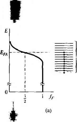 Allowed - energy states 4.7 Summary 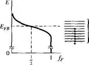 A По wed energy states fa = ;---E Figure 4.20 i The Fermi energy of (a) material A in thermal equilibrium, (b) material В in thermal equilibrium, (c) materials A and В at the instant they are placed in contact, and (d) materials A and В in contact at thermal equilibrium. a function of energy, is the same in the two materials. This equilibrium state occurs when the Fermi energy is the same in the two materials as shown in Figure 4.20d. The Fermi energy, important in the physics of the semiconductor also provides a good pictorial representation of the characteristics of the semiconductor materials and devices. 4.7 I SUMMARY The concentration of electrons in the conduction band is the integral over the conduction band energy of the product of the density of states function in the conduction band and the Fermi-Dirac probability function. The concentration of holes in the valence band is the integral over the valence band energy of the product of the density of states function in the valence band and the probability of a state being empty, which is[l - ff{E)\. Ш Using the MaxweJt-Boltzmann approximation, the thermal equilibrium concentration of electrons in the conduction band is given by По N,. exp -JE, - Ef) kT where iV is the effective density of states in the conduction band. 7671 Using the Maxwell-Boltzmann approximation, the thermal equilibrium concentration of holes in the valence band is given by po Nl, exp where Nj, is the effective density of states in the valence band. The intrinsic carrier concentration is found from ; = N /V,; exp The concept of doping the semiconductor with donor (group V elements) impurities and acceptor (group III elements) impurities to form n-type and p-type extrinsic semiconductors was discussed. The fundamental relationship of = 7 was derived. Using the concepts of complete ionization and charge neutrality, equations for the electron and hole concentratiotis as a function of impurity doping concentrations wei derived. The position of the Fermi energy level as a function of impurity doping concentrati( was derived. The relevance of the Fermi energy was discussed. The Fermi energy is a constant throughout a semiconductor that is in thermal equilibrium. GLOSSARY OF IMPORTANT TERMS acceptor atoms Impurity atoms added to a semiconductor to create a p-type material. charge carrier The electron and/or hole that moves inside the semiconductor and gives rise to electrical currents. compensated semiconductor A semiconductor that contains both donors and acceptors ij the same semiconductor region. complete ionization The condition when all donor atoms are positively charged by givij up their donor electrons and all acceptor atoms are negatively charged by accepting electrc degenerate semiconductor A semiconductor whose eleclron concentration or hole com tration is greater than the effective density of states, so that the Fermi level is in ihe con< tion band (n type) or in the valence band (p type). donor atoms Impurity atoms added to a semiconductor to create an n-type material. effective density of states The parameter , which results from integrating the densit quantum states gdE) times the Fermi function fy(E) over the conduction-band energy, the parameter /V , which results from integrating the density of quantum states gdE) lit [1 - friE)] over the valence-band energy. extrinsic semiconductor A semiconductor in which controlled amounts of donors anc acceptors have been added so that the electron and hole concentrations change from the ij trinsic carrier concentration and a preponderance of either electrons (n type) or holes (p t) is created. freeze-out The condition that occurs in a semiconductor when the temperature is low( and the donors and acceptors become neutrally charged. The electron and hole concenut become very small. Review Questions 147 mtrinsic carrier concentration tii The electron concentration in the conduction band and the hole concentration in the valence band (equal values) in an intrinsic semiconductor. intrinsic Fermi level Epi The position of the Fermi level in an intrinsic semiconductor. intrinsic semiconductor A pure semiconductor material with no impurity atoms and no lattice defects in the crystal. nondegenerate semiconductor A semiconductor in which a relatively small number of donors and/or acceptors have been added so that discrete, noninteracting donor states and/or discrete, noninteracting acceptor states are introduced. CHECKPOINT After studying this chapter, the reader should have the ability to: Derive the equations for the thermal equilibrium concentrations of electrons and holes in terms of the Fermi energy. Derive the equation for the intrinsic carrier concentration. State the value of the intrinsic carrier concentration for silicon at Г = 300 К. Derive the expression for the intrinsic Fermi level. Describe the effect of adding donor and acceptor impurity atoms to a semiconductor. Understand the concept of complete ionization. Understand the derivation of the fundamental relationship npo = n, Describe the meaning of degenerate and nondegenerate semiconductors. Discuss the concept of charge neutrality. Derive the equations for о and po in terms of impurity doping concentrations. Discuss the variation of the Fermi energy with doping concentration and temperature. REVIEW QUESTIONS 1. Write the equation for n{E) as a function of the density of states and the Fermi probability function. Repeat for the function p{E), 2. In deriving the equation for щ in terms of the Fermi function, the upper limit of the integral should be the energy at the top of the conduction band. Justify using infinity instead. 3. Assuming the Boltzmann approximation applies, write the equations for щ and po in terms of the Fermi energy. 4. What is the value of the intrinsic carrier concentration in silicon at Г = 300 K? 5. Under what condition would the intrinsic Fermi level be at the midgap energy? 6. What is a donor impurity? What is an acceptor impurity? 7. What is meant by complete ionization? What is meant by freeze-out? 8. What is the product of щ and po equal to? 9. Write the equation for charge neutrality for the condition of complete ionization. 10. Sketch a graph of no versus temperature for an n-type material. 11. Sketch graphs of the Fenui energy versus donor impurity concentration and versus temperature. PROBLEMS Section 4Л Charge Carriers in Semiconductors 4.1 Calculdte the intrinsic canrier concentration, л at = 200,400, and 600 К for {a) silicon, (h) gennanium, and (c) gallium arsenide. 4.2 The intrinsic carrier concentration in silicon i.s to be no greater than fif = \ x 10 cm- . Assume Eg = 1.12 eV. Determine the maximum temperature allowed the silicon. 4.3 Plot the intrinsic carrier concentration, fij, for a temperature range of 200 <T < 600 К for (й) silicon, ib) germanium, and (c) gallium arsenide. (Use a log scale for rt /.) 4.4 In a particular semiconductor material, the effective density of states functions are given by N = N-oiT) and N. = N.iTf- where /V-o and iV () are constants independent of temperature. The experimentally determined intrinsic carrier concentiJ tions as a function of temperature are given in Table 4.5. Determine the product NcoN.Q and the bandgap energy Eg. (Assume E is independent of temperature.) 4.5 (a) The magnitude of the product gc{E)ff{E) in the conduction band is a functioni energy as shown in Figure 4.1. Assume the Boltzmann approximation is valid. Deter mine the energy with respect to E, at which the maximum occurs. (i>) Repeat pan (a for the magnitude of the product v(£) [1 fy{E)\ in the valence band. 4.6 Assume the Boltzmann approximation in a semiconductor is valid. Determine the ratio of rt(£) = gc{E)fr{E) at £ = E, + 4АГ to that at £ = E, + kTfl. \ 4.7 Assume that E - Ef = 0.20 eV in sihcon. Plot n{E) = gc iE)ff(E) over the ran £, + 0.10 eV for (a) Г = 200 К and ф) Г = 400 К. \ 4-8 Two semiconductor materials have exactly the same properties except that materials has a bandgap energy of 1.0 eV and material В has a bandgap emrgy of 1.2 eV. Dcic mine the ratio of / of material A to that of material В for Г = 300 К, 4.9 [a) Consider silicon at T - 300 K. Plot the thermal equiUbrium eleclron concentration (on a log scale) over the energy range 0,2 < - Ef < 0.4 eV. (i?) Repeat part {a) for the hole concentration over the range 0.2 < Ef - < 0.4 eV. 4.10 Given the effective masses of electrons and holes in silicon, germanium, and galliuir arsenide, calculate the position of the intrinsic Fermi energy level with respect to the center of the bandgap for each semiconductor at T = 300 K. 4Л1 (a) The carrier effective masses in a semiconductor are = 0.62/rto and m* = I .4ju Determine the position of the intrinsic Fermi level with respect to the center of the bandgap at 7 = 300 K. (b) Repeat part (a) ifm = 1. Ют and = 0.25wo- j Table 4.51 Intrinsic concentration as a function of temperature
1 ... 12 13 14 15 16 17 18 ... 55 |
|
© 2026 AutoElektrix.ru
Частичное копирование материалов разрешено при условии активной ссылки |