 |
 |
 |
| Главная Журналы Популярное Audi - почему их так назвали? Как появилась марка Bmw? Откуда появился Lexus? Достижения и устремления Mercedes-Benz Первые модели Chevrolet Электромобиль Nissan Leaf |
Главная » Журналы » Absorbing materialorganic polymer 1 ... 14 15 16 17 18 19 20 ... 55 perfect periodic potential function. A perfect periodic potential in a solid allows electrons to move unimpeded, or with no scattering, through the crystal. But the thermal vibrations cause a disruption of the potential function, resulting in an interaction between the electrons or holes and the vibrating lattice atoms. This lattice scattering is also referred to as phonon scattering. Since lattice scaiiQvmg is related to the thermal motion of atoms, the rate at which the scattering occurs is a function of temperature. If we denote pi as the mobility that would be observed if only lattice scsAiermg existed, then the scattering theory states that to first order PL ОС T (5.15) Mobility that is due to lattice scattering increases as the temperature decreases. Intuitively, we expect the lattice vibrations to decrease as the temperature decreases, which implies that the probability of a scattering event also decreases, thus increasing mobility. Figure 5.2 shows the temperature dependence of electron and hole mobitides in silicon. In lightly doped semiconductors, lattice scattering dominates and the carrier mobility decreases with temperature as we have discussed. The temperature dependence of mobility is proportional to The inserts in the figure show that the parameter n is not equal to as the hrst-order scattering theory predicted. However, mobility does increase as the temperature decreases. The second interacrion mechanism affecting carrier mobility is called ionized impurity scattering. We have seen that impurity atoms are added to the semiconductor to control or alter its characteristics. These impurities are ionized at room temperature so that a coulomb interaction exists between the electrons or holes and the ionized impurities. This coulomb interaction produces scattering or collisions and also alters the velocity characteristics of the charge carrier. If we denote д / as the mobility that would be observed if only ionized impurity scattering existed, then to first order we have tii ОС -- (5.16) where N1 = N N is the total ionized impurity concentration in the semiconductor. If temperature increases, the random thermal velocity of a carrier increases, reducing the time the carrier spends in the vicinity of the ionized impurity center. The less time spent in the vicinity of a coulomb force, the smaller the scattering effect and the larger the expected value of Д/. If the number of ionized impurity centers increases, then the probability of a carrier encountering an ionized impurity center increases, implying a smaller value of д /. Figure 5.3 is a plot of electron and hole mobilities in germanium, silicon, and gallium arsenide at T = 300 К as a function of impurity concentration. More accurately, these curves are of mobility versus ionized impurity concentration Nj. As the impurity concentration increases, the number of impurity scattering centers increases, thus reducing mobility. 5000 2000 1000 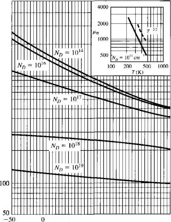 1000 50 100 (Л > в 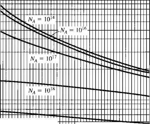 И) -50 ККК) 2(Х)
ПК) 200 500 lono о 50 100 Figure 5.2 flrrirtin and {ЬНпок- mnliliiiL-s in silicon versus temperature for various doping concentrations. Inserts show lempcraUirc lI h > I JIJ11 к > Ч t I i I ML I  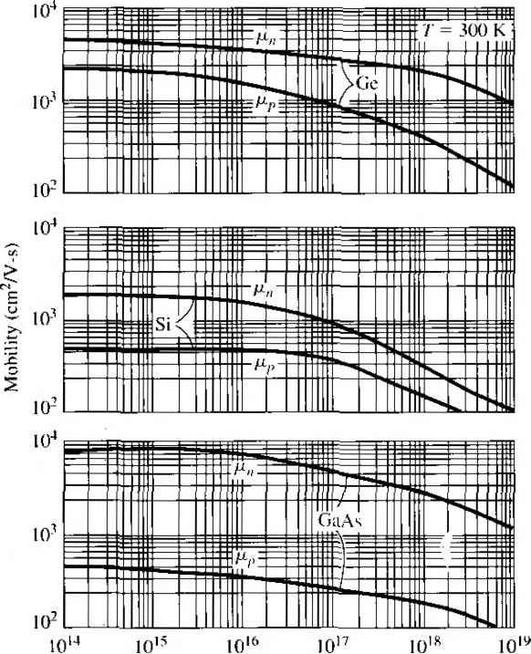 Impurity concentration (СТП -) Figure 5.3 I Electron and hole mobilities versus impurity concentrations for germanium, silicon, and gallium arsenide at Г = 300 К. (FromSzefllJ.) TEST YOUR UNDERSTANDING E5.3 (a) Using Figure 5.2, find the electron mobility for (i) N,{ = W cmKT = 15(ГС and 00 = I0 cm\ T = OC. (h) Find the hole mobilities for (/) N, = 104m-\ T = 50 C; and ( ) N, = 10 cm-\ T = \50C. [s-A/jUiDOoZ- 0.0 -A/uio 08£- 0) (q) -A/oool- (./) -душо oo£ 0) 0) *иу] E5.4 Using Figure 5.3, determine the electron and hole mobihties in (a) silicon for Af = 10 cm--\ Л^ = 0; (b) silicon for Nj = 10 cm-\ N, = 5 x 10 cm ; (c) silicon for Ni = cm- Л^, = 10 cm -\ and (d) GaAs for Nj = N = 10 cm-\ [-Л/шэ qzz rl Qogp ri (/?) ioie )08 P) ooe тУ w (я) mv = Ъя£\ (?) -suvj If Ti is the mean time between collisions due to lattice scattering, then clt/zt is the probability of a lattice scattering event occurring in a differential time dt. Likewise, if г/ is the mean time between collisions due to ionized impurity scattering, then dt/ti is the probabiUty of an ionized impurity scattering event occurring in ifi. differential time Л If these two scattering processes are independent, then the tot;i probability of a scattering event occurring in the differential time dt\s the sum of tfi individual events, or dt dt dt - = - + - T Г/ Tl where r is the mean time between any scattering event. Comparing Equation (5.17) with the definitions of mobility given by Equa tion (5.13) or (5.14), we can write (5. IS where д/ is the mobility due to the ionized impurity scattering process and fii isth mobility due to the lattice scattering process. The parameter is the net mobilit} With two or more independent scattering mechanisms, the inverse mobilides adu which means that the net mobility decreases. 5.1.3 Conductivity The drift current density, given by Equation (5.9), may be written as Jdrf = (ДнП + Mp/?)E = aE (5.1V where a is the conductivity of the semiconductor material. The conducrivity is give: in units of (Q-cm)~ and is a function of the electron and hole concentrations and mo bilities. We have just seen that the mobilities are functions of impurity concentration conductivity, then is a somewhat complicated function of impurity concentration. The reciprocal of conductivity is resistivity, which is denoted by p and is give in units of ohm-cm. We can write the formula for resistivity as a е{р.пП + PpP) (5.2i Figure 5.4 is a plot of resistivity as a function of impurity concentration in silicor germanium, gallium arsenide, and gallium phosphide at Г = 300 К. Obviously, th curves are not linear functions of Nj or /V because of mobility effects. If we have a bar of semiconductor material as shown in Figure 5.5 with a vo age applied that produces a current /, then we can write (5.21a (5.21bj 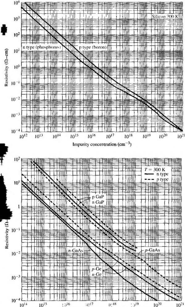 1016 ,017 loK lo Impurity concentration (cm~-) Figure 5.4 I Resistivity versus impurity concentration at 7 = 300 К in (a) silicon and (b) gennanium, gallium arsenide, and gallium phosphide. (From Szellll) 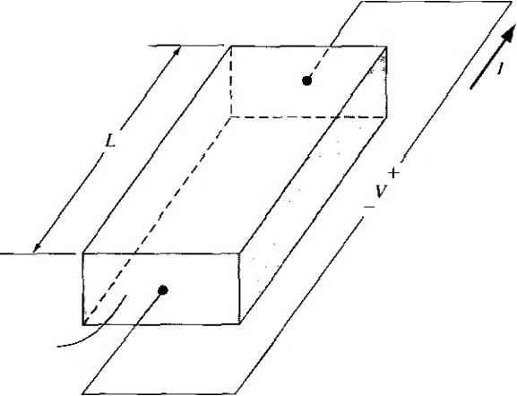 Area л Figure 5.5 I Bar of semiconductor material as a resistor We can now rewrite Equation (5.19) as  (52: Equation (5.22b) is Ohms law for a semiconductor. The resistance is a function of resistivity, or conductivity, as well as the geometry of the semiconductor If we consider, for example, a p-type semiconductor with an acceptor doping [Nj - 0) in which Na ft/, and if we assume that the electron and hole mobilities are of the same order of magnitude, then the conductivity becomes If we also assume complete ionization, then Equation (5.23) becomes (5.23): (5.24) The conductivity and resistivity of an extrinsic semiconductor are a function pri-luarily of the majority carrier parameters. We may plot the carrier concentration and conductivity of a semiconductor as a funcrion of temperature for a particular doping concentration. Figure 5.6 shows the electron concentration and conductivity of silicon as a function of inverse temperature for the case when Ni = Ю^* cm\ In the midtemperature range, or extrinsic range, as shown, we have complete ionization-the electron concentration remains essentially constant. However, the mobility is a function of temperature so the conductivity 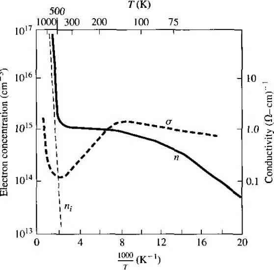 Figure 5.6 I Electron concentration and conductivity versus inverse temperature for silicon. (After Szefll].) varies with temperature in this range. At higher temperatures, the intrinsic carrier concentration increases and begins to dominate the electron concentration as well as the conductivity. In the lower temperature range, freeze-out begins to occur; the electron concentration and conductivity decrease with decreasing temperature. Objectivl EXAMPLE 5.2 To determine the doping concentration and majority carrier mobility given the type and conductivity of a compensated semiconductor. Consider compensated n-type silicon at Г = 300 К, with a conductivity of rr 16(-cm)~ and an acceptor doping concentration of 10 cm~-. Determine the donor с centration and the electron mobility. con- Solution For n-type silicon at 7 = 300 K, we can assume complete ionization; therefore the conductivity, assuming - N. > , is given by We have that 16 = (1.6 X 10-) ,(AV - 10) Since mobility is a function of the ionized impurity concentration, we can use Figure 5.3 along with trial and error to detennine Pn and A. For example, if we choose Ni =2 x 10, then Nj = + =3x10 so that fi 510 cm/V-s which gives a = 8.16 (Q-cm)-If we choose N,i = 5 к J0\ then Nf = 6 x 10 so that ju 325 cmVV-s, which gii fT = 20.8 (-cm)~V The doping is bounded between these two values. Further trial and yields 3.5 X 10 cm- which gives д„ 400cmVV-s (716 (-cm) Comment We can see from this example that, in high-conductivity semiconductor material, mobility isi strong function of carrier concentration. DESIGN EXAMPLE 5.3  Objective To design a semiconductor resistor with a specified resistance to handle a given current densi A silicon semiconductor at T = 300 К is initially doped with donors at a concentratioin iV = 5 X 10 cm~-. Acceptors are to be added to form a compensated p-type material. Th resistor is to have a resistance of 10 and handle a current density of 50 A/cnr when 5 V applied. Solution For 5 V applied to a 10-kQ resistor, the total current is V 5 / = -- = - = 0.5 mA R 10 If the current density is limited to 50 A/cnr, then the cross-sectional area is / 0.5 X 10- , , =---= 10 cm J 50 If we, somewhat arbitrarily al this point, limit the electric field to E = 100 V/cm, then length of the resistor is L = - = -- =5x 10 cm E 100 From Equation (5.22b), the conductivity of the semiconductor is 5 X 10-- RA (10)(10--) = 0.50 (Q-cm) The conductivity of a compensated p-type semiconductor is where the mobility is a function of the total ionized impurity concentration jV, H- jVj. Using trial and error, if = K25 x 10 cm-\ then N +/V = 1.75 x 10 cm-\ and the hole mobility, from Figure 5.3, is approximately fip =410 cnr/\-s. The conductivity is then o=e,{K-Nj) = (\,6x 10-)(410)(1.25 x 10 - 5 x lO) = 0.492 which is very close to the value we need. Comment Since the mobility is related to the total ionized impurity concentration, the determination of (he impurity concentration to achieve a particular conductivity is not straightforward. TEST YOUR UNDERSTANDING E5.5 Silicon at Г = 300 К is doped with impurity concentrations of Nj =5 x lO* cm and Ni, -1 X 10 cm. (<з) What are the electron and hole mobilities? (h) Determine the conductivity and resistivity of the material, [шэ- SOZO = 8> = -о iq) Qg£ = rf s-A/uiD qoOI = ( ) *suv] E5.6 For a particular silicon semiconductor device at Г = 300 К, the required material is n type with a resistivity of 0.10 -cm, (a) Determine the required impurity doping concentration and (b) the resulting electron mobility. [5-д/шэдб9 (Я) у,01 X 6 Л/ эгпЗы W suy] E5.7 A bar of p-typc silicon, such as shown in Figure 5.5, has a cross-sectional area of A = 10~ cm- and a length of L = 1.2 x 10 - cm. For an applied voltage of 5 V, a current of 2 mA is required. What is the required (a) resistance, (h) resistivity of the silicon, and (c) impurity doping concentration? U-iciOf (J)iitsшг(q)ятWuy] For an intrinsic material, the conductivity can be written as = eifin + fip)ni (5.25) The concentrations of electrons and holes are equal in an intrinsic semiconductor, so the intrinsic conductivity includes both the electron and hole mobility. Since, in general, the electron and hole mobilities are not equal, the intrinsic conductivity is not the minimum value possible at a given temperature. 5ЛЛ Velocity Saturation So far in our discussion of drift velocity, we have assumed that mobility is not a function of electric field, meaning that the drift velocity will increase linearly with applied electric field. The total velocity of a particle is the sum of the random thermal velocity and drift velocity. At T = 300 K, the average random thermal energy is given by kmvfi = UT i(0.0259) 0.03885 eV (5.26) о > -О 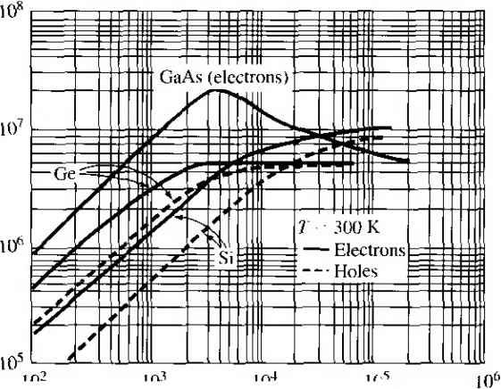 10 10-* 10- Electric field (V/cm) Figure 5.7 I Carrier drift velocity versus electric field for high-purity silicon, germanium, and gallium arsenide. (Fmm Sze 1121) This energy translates into a mean thermal velocity of approximately 10 cm/s for ал electron in silicon. If we assume an electron mobility of д„ = 1350 cm/V-s in low doped silicon, a drift velocity of 10 cm/s, or 1 percent of the thermal velocity, i achieved if the applied electric field is approximately 75 V/cm, This applied electric field does not appreciably alter the energy of the electron. Figure 5.7 is a plot of average drift velocity as a function of applied electric field for electrons and holes in silicon, gallium arsenide, and germaniuiu. At low electric fields, where there is a linear variation of velocity with electric field, the slope of the drift velocity versus electric field curve is the mobility. The behavior t)f the drift velocity of carriers at high electric fields deviates substantially from the linear relationship observed at low fields. The drift velocity of electrons in silicon, for example, saturates at approximately 10 cm/s at an electric field of approximately 30 kV/cm. If the drift velocity of a charge carrier saturates, then the drift current density also saturates and becomes independent of the applied electric field. The drift velocity versus electric field characteristic of gallium arsenide is mere complicated than for sihcon or germanium. At low fields, the slope of the drift velocity versus E-field is constant and is the low-field electron mobility, which is ap-proxinately 8500 cnr/V-s for gallium arsenide. The low-field electron mobility in gallium arsenide is much larger than in silicon. As the field increases, the electron drift velocity in gallium arsenide reaches a peak and then decreases. A differential mobility is the slope of the versus E curve at a particular point on the curve afld the negative slope of the drift velocity versus electric field represents a negative differential mobility. The negative differential mobility produces a negative differential resistance; this characteristic is used in the design of oscillators. 1 ... 14 15 16 17 18 19 20 ... 55 |
||||||||||||||||||||||||||||||||||||||||||||||||||||||||||||||||||||||||||||||||||||||
|
© 2026 AutoElektrix.ru
Частичное копирование материалов разрешено при условии активной ссылки |