 |
 |
 |
| Главная Журналы Популярное Audi - почему их так назвали? Как появилась марка Bmw? Откуда появился Lexus? Достижения и устремления Mercedes-Benz Первые модели Chevrolet Электромобиль Nissan Leaf |
Главная » Журналы » Absorbing materialorganic polymer 1 ... 15 16 17 18 19 20 21 ... 55 GaAs Conduction band 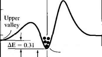 Lower valley  Valence band 1111 flOO Figure 5.8 I Energy-band structure for gallium arsenide showing the upper valley and lower valley in the conduction band. (From Sze fJ3].) The negative differential mobility can be understood by considering the E versus к diagram for gallium arsenide, which is shown again in Figure 5.8. The density of states effective mass of the electron in the lower valley is m* = 0.067/ио- The small effective mass leads to a large mobility. As the E-field increases, the energy of the electron increases and the electron can be scattered into the upper valley, where the density of states effective mass is 0.55шо. The larger effective mass in the upper valley yields a smaller mobility. This intervaJley transfer mechanism resuUs in a decreasing average drift velocity of electrons with electric field, or the negative differential mobility characteristic. 5.2 I CARRIER DIFFUSION There is a second mechanism, in addition to drift, that can induce a current in a semiconductor. We may consider a classic physics example in which a container, as shown in Figure 5.9, is divided into two parts by a membrane. The left side contains gas molecules at a particular temperature and the right side is initially empty. The gas molecules are in continual random thermal motion so that, when the membrane is broken, the gas molecules flow into the right side of the container Diffusion is the process whereby particles flow from a region of high concentration toward a region of low 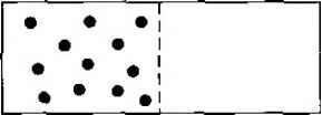 x = 0 Figure 5.9 I Container divided by a membrane with gas molecules on one side. 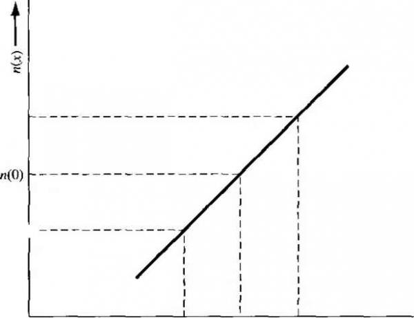 n(-l) - x= -I x = 0 x= +1 Figure 5.101 Electron concentration versus distance. concentration. If the gas molecules were electrically charged, the net flow of cl would result in a diffusion current. 5,2.1 Diffusion Current Density To begin to understand the diffusion process in a semiconductor, we will consider simplified analysis. Assume that an electron concentration varies in one dimensioii shown in Figure 5.10. The temperature is assumed to be uniform so that the averaj diermal velocity of electrons is independent of x. To calculate the current, we willdq termine the net flow of electrons per unit time per unit area crossing the plane al X - 0. If the distance / shown in Figure 5.10 is the mean-free path of an electron, thj is, the average distance an electron travels between collisions (/ - VtiZcn), then с the average, electrons moving to the right at jc = -I and electrons moving to the к at л - +/ will cross the Jt =0 plane. One half of the electrons at jc - -/ will be tra eling to the right at any instant of tiine and one half of the electrons atx = -hi will bj traveling to the left at any given time. The net rate of electron flow, F , in the Fij direction at л - 0 is given by (5.27) If we expand the electron concentration in a Taylor series about jr = 0 keeping only the first two terms, then we can write Equation (5.27) as пф)-1 dn d dn dx (5.28) which becomes Fn = -VtiJ dn dx (5.29) Each electron has a charge (-e), so the current is J = -eFfi - +evthl dn dx (5.30) The current described by Equation (5.30) is the electron diffusion current and is proportional to the spatial derivative, or density gradient, of the electron concentration. The diffusion of electrons from a region of high concentration to a region of low concentradon produces a flux of electrons flowing in the negative x direction for this example. Since electrons have a negative charge, the conventional current direction is in the positive x direction. Figure 5.11a shows these one-dimensional flux and current directions. We may write the electron diffusion current density for this one-dimensional case, in the form dn dx (5.31) where D is called the electron diffusion coefficient, has units of cnr/s, and is a positive quantity. If the electron density gradient becomes negative, the electron diffusion current density will be in the negative jc direction. Figure 5.11b shows an example of a hole concentration as a function of distance in a semiconductor. The diffusion of holes, from a region of high concentration to a region of low concentration, produces a flux of holes in the negative x direction. Since holes are positively charged particles, the conventional diffusion current density is also in the negative x direction. The hole diffusion current density is proportional to the hole density gradient and to the electronic charge, so we may write
с о С о с с tj о  с о с и Electron flux Electron diffusion current density  Hole llux Hoie diffusion current density Figure 5.111 (a) Diffusion of electrons due to a density gradient, (b) Diffusion of holes due to a density gradient. for the one-dimensional case. The parameter Dp is called the hole diffusion coel cient, has units of cm/s, and is a positive quantity. If the hole density gradient comes negative, the hole diffusion current density will be in the positive x directic EXAMPLE 5.4 Objective To calculate the diffusion current density given a density gradient. Assume that, in an n-type gallium arsenide semiconductor at T = 300 K, the elec concentration varies linearly from I x 10 to 7 x 10 cm -* over a distance of 0.10 cm. Ca culate the diffusion current density if the electron diffusion coefficient is D = 225 cm-/s. Solution The diffusion current density is given by dn An Jn\dif =eD - eD - = (L6 x 10-)(225) X 10 - 7 X 10 0.10 = 108 A/cm Comment A significant diffusion current density can be generated in a semiconductor material witho a modest density gradient. TEST YOUR UNDERSTANDING E5.8 The electron concentration i n si 1 icon i s gi ven by л (л) = 10 г' cm ~ (л > 0) where = 10 cm. The electron diffusion coefficient is = 25 cm/s. Determine the electron diffusion current density ai (a) ,v =0,(b)x = 10 * cm, and (c) x -> oc. E5.9 The hole concentration in silicon varies linearly from x 0 to x = O.Ol cm. The hole diffusion coefficient is Dp = 10 cm-/s, the hole diffusion current density is 20 A/cm , and the hole concentration atjt:=0isp = 4xl0 cm~-. What is the value of the hole concentration at л- =0.01 cm? (е-ШЗ , jOl x fiz suy) Е5Л0 The hole concentration in silicon is given by p(x) = 2 x е~р^ cwT {x > 0). The hole diffusion coefficient is Dp = lOcm/s. The value of the diffusion current density at .y = 0 is Jjif = +6.4 A/cm-. What is the value of L? (шл . ot X g = 7 suy) 5.2.2 Total Current Density We now have four possible independent current mechanisms in a semiconductor. These components are electron drift and diffusion currents and hole drift and diffusion currents. The total current density is the sum of these four components, or, for the one-dimensional case, dn dp J enii E -h epfij,E , -\-eD ---L) - (5.33) dx dx This equation may be generalized to three dimensions as J = enfinE-\- epfjipE + еО,Уп - eDVp (5.34) The electron mobility gives an indication of how well an electron moves in a semiconductor as a result of the force of an electric field. The electron diffusion coefficient gives an indication of how well an electron moves in a semiconductor as a result of a density gradient. The electron mobility and diffusion coefficient are not independent parameters. Similarly, the hole mobility and diffusion coefficient are not independent parameters. The relationship between mobility and the diffusion coefficient will be developed in the next section. The expression for the total current in a semiconductor contains four terms. Fortunately in most situations, we will only need to consider one term at any one time at a particular point in a semiconductor. 5.3 I GRADED IMPURITY DISTRIBUTION In most cases so far, we have assumed that the semiconductor is uniformly doped. In many semiconductor devices, however, there may be regions that are nonuniformly doped. We will investigate how a nonuniformly doped semiconductor reaches thermal equilibrium and, from this analysis, we will derive the Einstein relation, which reh mobility and the diffusion coefficient. 5.3.1 Induced Electric Field Consider a semiconductor that is nonuniformly doped with donor impurity atoms. the semiconductor is in thermal equilibrium, the Fermi energy level is со: through the crystal so the energy-band diagram may qualitatively look like 1:1.1 shown in Figure 5.12. The doping concentration decreases as jt increases in this aise There will be a diffusion of majority carrier electrons from the region of high con centration to the region of low concentration, which is in the +x direction. The IIov of negative electrons leaves behind positively charged donor ions. The separaiinn 0 positive and negative charge induces an electric field that is in a direction to ор[Ч1м the diffusion process. When equilibrium is reached, the mobile carrier concent ran or is not exactiy equal to the fixed impurity concentration and the induced electric tick prevents any further separation of charge. In most cases of interest, the space chm induced by this diffusion process is a small fraction of the impurity concentratl( thus the mobile carrier concentration is not too different from the impurity do\ density. The electric potential ф is related to electron potential energy by the ch< (-), so we can write The electric field for the one-dimensional situation is defined as £1ф 1 dEfi Ev =-- = - dx e dx .51; ш-т' Figure 5.12 [ Energy-band diagram for a semiconductor in thermal equilibrium with a nonuniform donor impurity concentration. If the intrinsic Fermi level changes as a function of distance through a semiconductor in thermal equilibrium, an electric held exists in the semiconductor. If we assume a quasi-neutrality condition in which the electron concentration is almost equal to the donor impurity concentration, then we can still write По = rij exp Solving for Ef - Efi, we obtain Ef - Efi If NAx) (5.37) Ef - Efi = kT In y-j (5-) The Fermi level is constant for thermal equilibrium so when we take the derivative with respect to x we obtain dEfi kT dNd(x) --Г^ТТУТ-(5-39) dx Л'(л) dx The electric field can then be written, combining Equations (5.39) and (5.36), as кТ\ 1 dNAx) Ev , (5.40) e J Nx) dx Since we have an electric field, there will be a potential difference through the semiconductor due to the nonuniform doping. Objecrive example 5.5 To determine the induced electric field in a semiconductor in thermal equilibrium, given a linear variation in doping concentration. Assume that the donor concentradon in an n-type semiconductor at Г = 300 К is given by NAx) = 10 lOjc (cm-) where Jt is given in cm and ranges between 0 < x < I /im Solution Taking the derivative of the donor concentration, we have The electric field is given by Equation (5.40), so we have -(0.0259)(-10) Щ. ~ (10 - lOir) Al JC = 0, for example, wc find E, = 25.9 V/cm Comment Wc may recall from our previous discussion of drift current that fairly small electric fields< produce significant drift cuirent densities, so that an induced electric field from noniinifc doping can significantly influence semiconductor device characteristics. 5.3.2 The Einstein Relation If we consider the nonunifirmly doped semiconductor represented by the еш band diagram shown in Figure 5.12 and assume there are no electrical connections] that the semiconductor is in thermal equilibrium, then the individual electron hole currents must be zero. We can write dn dx If we assume quasi-neutrality so that n Л/,/(х), then we can rewrite Eqi tion (5.41) as Л = 0 = efx Ndix)Ej,. + eD dNAx) dx Subsrituting the expression for the electric field from Equation (5.40) into rion (5.42), we obtain 0= -e/iNdix) 1 dNdU) dNM) Nd{x) dx Equation (5.43) is valid for the condition The hole current must also be zero in the semiconductor. Froiu this condit we can show that D, kT Combining Equations (5.44a) and (5.44b) gives Ц„ pp The diffusion coefficient and mobility are not independent parameters. This rek between the mobility and diffusion coefficient, given by Equation (5.45), is knoi the Einstein relation. 5.4 The Hall Effect 177 Table 5.2 I Typical mobility and diffusion coefficient values at Г = 300 К (/i cm-A-s and D = cmVs)
Objective EXAMPLE 5.6 To determine the diffusion coefficient given the carrier mobility. Assume that the mobility of a particular carrier is 1000 cm-A-s at Г = 300 К. Solution Using the Einstein relation, we have that D = j = (0,0259)(1000) = 25.9 cnr/s Comment Although this example is fairly simple and straightforward, it is important to keep in mind the relative orders of magnitude of the mobility and diffusion coefficient. The diffusion coefficient is approximately 40 limes smaller than the mobility al room temperature. Table 5.2 shows the diffusion coefficient values at T - 300 К corresponding to the mobihfies listed in Table 5.1 for silicon, gallium arsenide, and germanium. The relation between the mobility and diffusion coefficient given by Equation (5.45) contains temperature. It is important to keep in mind that the major temperature effects are a result of lattice scattering and ionized impurity scattering processes, as discussed in Section 5.1.2. As the mobilities are strong functions of temperature because of the scattering processes, the diffusion coefficients are also strong functions of temperature. The specific temperature dependence given in Equation (5.45) is a small fraction of the real temperature characteristic. *5.4 I THE HALL EFFECT The Hall effect is a consequence of the forces that are exerted on moving charges by electric and magnetic fields. The Hall effect is used to distinguish whether a semiconductor is n type or p type* and to measure the majority carrier concentration and majority carrier mobility. The Hall effect device, as discussed in this section, is used to experimentally measure semiconductor parameters. However, it is also used extensively in engineering applications as a magnetic probe and in other circuit applicadons. *We will assume an extrinsic semiconductor material in which the majority carrier concentration is much l4han the minority carrier concentration. 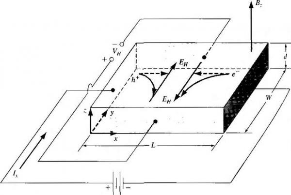 Figure 5.13 I Geometry for measuring the Hall effect. The force on a particle having a charge g and moving in a magnetic field is given by F qvx В (5.46) where the cross product is taken between velocity and magnetic field so that the force vector is perpendicular to both the velocity and magnetic field. Figure 5.13 dlustrates the Hall effect. A semiconductor with a current / placed in a magnetic field perpendicular to the current. In this case, the magnetic field is in the z direction. Electrons and holes flowing in the semiconductor will experience a force as indicated in the figure. The force on both electrons and holes is intk (-y) direction. In a p-type semiconductor (po > o), there will be a buildup of positive charge on the у = 0 surface of the semiconductor and, in an n-type semiconductor ( 0 > Po) there will be a buildup of negative charge on the у - 0 surface. This net charge induces an electric field in the y-di recti on as shown in the figure. In steady state, the magnetic field force will be exactly balanced by the induced electric field force. This balance may be written as Fq[E + vx B]=0 (5.47a) which becomes E, QVyB, (5.47b) The induced electric field in the y-direction is called the Hall field The Hall field produces a voltage across the semiconductor which is called the Hall voltage. We can write = +Ея W (5.48) 1 ... 15 16 17 18 19 20 21 ... 55 |
|
© 2026 AutoElektrix.ru
Частичное копирование материалов разрешено при условии активной ссылки |