 |
 |
 |
| Главная Журналы Популярное Audi - почему их так назвали? Как появилась марка Bmw? Откуда появился Lexus? Достижения и устремления Mercedes-Benz Первые модели Chevrolet Электромобиль Nissan Leaf |
Главная » Журналы » Absorbing materialorganic polymer 1 ... 16 17 18 19 20 21 22 ... 55 The hole mobility is then given by ep Wd Similarly for an n-type semiconductor, the low-field electron mobility is determii from - \7 TI/J enVj,.Wd EXAMPLE 5.7 Objective To determine the majority carrier concentration and mobihty, given Hall effect parameten Consider the geometry shown in Figure 5.13. Let L = \0~ cm, W = \0~ cm, d = 10 cm. Also assume that 7, 1.0 mA, V, = 12.5 V, B, = 500 gauss = 5 x 10 U and = -6.25 mV. Solution A negative Hall vohage for this geometry implies that we have an n-type semiconduc Using Equation (5.54), we can calculate the electron concentration as -(10-)(5x 10-Ъ - 3 . uxlO-)(10-)(-6.25xlO-)=- =5x10 cm The electron mobility is then determined from Equal ion (5.58) as (10-)(10-) (1.6 X 10 )(5x 10-)(12.5)(10-)(10-) - - p 1000 cm-/V-s Comment It is important to note that the MKS units must be used consistently in the Hall effect equati to yield correct results. 5.5 1 SUMMARY The two basic transport mechanisms are drift, due to an applied electric field, and diffusion, due to a density gradient. Carriers reach an average drift velocity in the presence of an applied electric field, di to scattering events. Two scattering processes within a semiconductor are lattice scattering and impurity scattering. The average drift velocity is a linear function of the applied electric field for small values of electric field, but the drift velocity reaches a saturafion limit that is on the . order of 10 cm/s at high electric fields, M Checkpoint 181 Carrier mobility is the ratio of the average drift velocity and applied electric field. The electron and hole mobilities are functions of temperature and of the ionized impurity concentration. The drift current density is the pnxluct of conductivity and electnc field (a form of Ohms law). Conductivity is a function of the carrier concentrations and mobilities. Resistivity is the inverse of conductivity, В The diffusion current density is proportional to the carrier diffusion coefficient and the carrier density gradient. I The diffusion coefficient and mobility are related through the Einstein relation. The Hall effect is a consequence of a charged carrier moving in the presence of perpendicular electric and magnetic fields. The charged carrier is deflected, inducing a Hall voltage. The polarity of the Hall voltage is a function of the semiconductor conductivity type. The majority carrier concentration and mobihty can be determined from the Hall voltage. GLOSSARY OF IMPORTANT TERMS conductivity A material parameter related to carrier drift; quantitatively, the ratio of drift current density to electric field. diffusion The process whereby particles flow from a region of high concentration to a region of low concemrafion. difTusion coeHicient The parameter relating particle flux to the particle density gradient. diffusion current The current that results from the diffusion of charged particles. drift The process whereby charged particles move while under the influence of an electric field. drift current The current that results from the drift of charged particles. drift velocity The average velocity of charged particles in the presence of an electric field. Einstein relation The relation between the mobility and the diffusion coefficient. Hall voltage The voltage induced across a semiconductor in a Hall effect measurement. ionized impurity scattering The interaction between a charged carrier and an ionized impurity center. lattice scattering The interaction between a charged carrier and a thermally vibrating lattice atom. mobility The parameter relating carrier drift velocity and electric field. resistivity The reciprocal of conductivity; a material parameter that is a measure of the resistance to cunrent. velocity saturation The saturation of cairicr drift velocity with increasing electric field. CHECKPOINT After studying this chapter, the reader should have the ability to: Discuss carrier drift current density. Explain why carriers reach an average drift velocity in the presence of an applied electric field. I Discuss the mechanisms of lattice scattering and impurity scattering. Define mobility and discuss the temperature and ionized impurity concentration dependence on mobility. Define conductivity and resistivity Discuss velocity saturation. Discuss carrier diffusion current density. State the Einstein relation. Describe the Hail effect. REVIEW QUESTIONS 1. Write the equation for the total drift current density. 2. Define carrier mobility. What is the unit of mobility? 3. Explain the temperature dependence of mobility. Why is the carrier mobility a fiincti of the ionized impurity concentrations? 4. Define conductivity. Define resistivity. What are the units of conductivity and resisti 5. Sketch the drift velocity of electrons in silicon versus electric field. Repeat for GaAs 6. Write the equations for the diffusion current densities of electrons and holes. 7. What is the Einstein relation? 8. Describe the Hall effect. 9. Explain why the polarity of the Hall voltage changes depending on the conductivity (n type or p type) of the semiconductor. PROBLEMS {Note: Use the semiconductor parameters given in Appendix В if the parameters are specifically given in a problem.) Section 5.1 Carrier Drift 5.1 Consider a homogeneous gallium arsenide semiconductor at 7 = 300 К with 10 cm and N = 0. (a) Calculate the thermal-equilibrium values of electron a hole concentrations, ib) For an applied E-field of 10 V/cm, calculate the drift силе density, (c) Repeat parts (a) and {b) if Nj = 0 and = 10 cm -. \ 5.2 A silicon crystal having a cross-sectional area of 0.001 cnr and a length of 10 cn connected at its ends to a 10-V battery. At 7 = 300 K, we want a current of 100 n in the silicon. Calculate: {a) the required resistance RAb) the required conductivit (c) the density of donor atoms to be added to achieve this conductivity, and {d) concentration of acceptor atoms to be added to form a compensated p-type ma with the conductivity given from part (b) if the initial concentration of donor at Nj = 10 cm--. 5.3 (a) A silicon semiconductor is in the shape of a rectangular bar with a cross-seclio area of 100 дт , a length of 0.1 cm, and is doped with 5 x 10 cm arsenic atoi The temperature is 7 = 300 K. Determine the current if 5 V is applied across the length, {b) Repeat part (a) if the length is reduced to 0.01 cm. (t) Calculate the average drift velocity of electrons in parts (a) and (/?). 5.4 (a) A GaAs semiconductor resistor is doped with acceptor impurities at a concent tion of iV = 10 cm -. The cross-sectional area is 85 finr. The current in the  Problems 183 resistor is to be / = 20 mA with 10 V applied. Determine the required length of the device, {h) Repeat part (a) for silicon. 5.5 (a) Three volts is applied across a 1-cm-long semiconductor ban The average electron drift velocity is 10 cm/s. Find the electron mobility, (b) If the electron mobility in part (a) were 800 cm~A-s, what is the average electron drift velocity? 5.6 Use the velocity-field relations for silicon and gallium arsenide shown in Figure 5.7 todetennine the transit time of electrons through a 1-/лп distance in these materials for an electric field of (a) 1 kV/cm and (h) 50 kV/cm. 5.7 A perfectly compensated semiconductor is one in which the donor and acceptor impurity concentrations are exactly equal. Assuming complete ionization, determine the conducrivity of silicon at T = 300 К in which the impurity concentrations are (a) N,=N = 10-* cm- and (b) N = jVj = lOcm \ 5.8 (a) In a p-type gallium arsenide semiconductor, the conductivity is a = 5 (-cm) at 7 = 300 K. Calculate the thermal-equifibriuin values of the electron and hole concentrations, (b) Repeat part (a) for n-type silicon if the resistivity is p = 8 -cm. 5.9 In a particular semiconductor material, д„ = 1000 cm/V-s, Pp = 600 cnrfW-% and Nc = Nv = 10* cm *. These parameters are independent of temperature. The measured conductivity of the intrinsic material is cr = 10~* (f2-cm)~ at Г = 300 К. Find the conductivity at Г = 500 К, 5.10 (a) Calculate the resistivity at Г - 300 К of intrinsic (/) silicon, ( ) germanium, and {iii) gallium arsenide. (7) If rectangular semiconductor bars are fabricated using the materials in part (a), determine the resistance of each bar if its cross-sectional area is 85 pm- and length is 200 m. 5.11 An n-type silicon sample has a resistivity of 5 -cm at Г = 300 К. (a) What is the donor impurity concentration? (b) What is the expected resistivity at (/) Г = 200 К and (/0 T = 400 K. 5.12 Consider silicon doped at impurity concenu-ations of Aj = 2 x 10 cm~* and /V = 0. An empirical expression relating electron drift velocity to electric field is given by  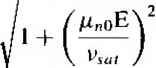 where д„о - 1350 cm /V-s, v,t - 1.8 x 10 cm/s, and E is given in V/cm. Plot electron drift current density (magnitude) versus electric field (log-log scale) over the range 0 < E < 10 V/cm. 5.13 Consider silicon at Г = 300 К. Assume the electron mobility is д„ = 1350 cm/V-s, The kinetic energy of an electron in the conduction band is (I /2)ml , where m* is the effective mass and is the drift velocity. Detemiine the kinetic energy of an electron in the conduction band if the applied electric field is (a) 10 V/cm and (b) 1 kV/cm. 5.14 Consider a semiconductor that is uniformly doped with = 10* cm * and = 0, with an applied electric field of E = 100 V/cm. Assume that д„ = 1000 cm/V-s and = 0. Also assume the following parameters: K=2x lOr/300)- cm- = I x IOr/300)/-cm- = 1.10 eV (a) Calculate the electric-current density at Г = 300 К. (b) At what temperature wil this current increase by 5 percent? (Assume the mobilities are independent of temperature.) 5.15 A semiconductor material has electron and hole mobilities (j. and respecti When the conductivity is considered as a function of the hole concentration po, (a) show that the minimum value of conductivity, Gi, can be written as j  2сг,(м /у) (M + M/>) where a, is the intrinsic conductivity, and (b) show that the corresponding hole concentration is po = i (м /Д/,). 5.16 A particular intrinsic semiconductor has a resistivity of 50 Q-cm alT = 300 К and! 5 QCm at Г = 330 К, Neglecting the change in mobility with temperature, detemj the bandgap energy of the semiconductor 5.17 Three scattering mechanisms are present in a particular semiconductor material. If only the first scattering mechanism were present, the mobility would be Д| = 2000 cm /V-s, if only the second mechanism were present, the mobility would be P2 1500 cmA-s, and if only the third mechanism were present, the mobility wt be дз = 500 cmA-s. What is the net mobility? 5.18 Assume that the mobility of electrons in silicon злТ = 300 К is /i = 1300 cmA Also assume that the mobility is limited by lattice scattering and varies as T~. Determine the electron mobility at (a) Г = 200 К and (b) T = 400 K. 5Л9 Two scattering mechanisms exist in a semiconductor. If only the first mechanism ц present, the mobility would he 250 cmVV-s. If only the second mechanism werep .sent, the mobility would be 500 cmVV-s. Determine the mobility when both scatto mechanisms exist at the same time, 5.20 The effective density of states functions in silicon can be written in the form  N, = 2.8 X 10 - /V. = 1.04 x 10  Assume the mobilities are given by -3/2 / 43/2 Assume the bandgap energy is £ = 1.12 eV and independent of temperature, the intrinsic conductivity as a function of Г over the range 200 <T< 600 K. 5.21 {a) Assume that the electron mobility in an n-type semiconductor is given by 1350 M = -r---T7T cm7V-s 1+ 5 X 10 where Nj is the donor concentration in cm \ Assuming complete ionization, plotl conductivity as a funcfion of over the range 10 < Nj < 10 cm~-. (b) Coi the results of part (a) to that if the mobility were assumed to be a constant equal Problems 1350 cmA-s. (c) If an electric field of F = 10 V/cm is applied to the semiconductor, plot the electron drift current density of parts (a) and (h). Section 5.2 Carrier Diffusion 5.22 5.23 5.25 5.26 5.27 5.28 Consider a sample of silicon at Г = 300 K. Assume that the electron concentration varies linearly with distance, as shown in Figure 5.14. The diffusion current density is found to be y,j = 0.19 A/cnr. If the electron diffusion coefficient is Д, = 25 cmVs, determine the electron concentration at x =0. The electron concentration in silic(?n decreases linearly from 10 cm to 10 ст over a distance of 0Л0 cm. The cross-sectional area of the sample is 0.05 cm~. The electron diffusion coefficient is 25 crnVs. Calculate the electron diffusion current. 5 The electron concentration in a sample of n-type silicon varies lineariy from 10 cm at X = 0 to 6 X 10 cm * at x = 4 pm. There is no applied electric field. The electron current density is experimentally measured to be - 400 A/cm. What is the electron diffusion coefficient? The hole concentration in p type GaAs is given by p 10(1 - x/L)cm~ for 0 < A < 1 where L - 10 дт. The hole diffusion coefficient is 10 cm /s. Calculate the hole diffusion current density at (й) Jt = 0, (/?) jc = 5 m, and {c) x = 10 дт. The hole concentration is given by p = 10 exp {-х/Ь^) cm~ for л > 0 and the electron concentrarion is given by 5 x 10 * exp (H-x/L ) cm~- for jt < 0. The values of L, and are 5 X 10 * cm and 10~ cm, respectively. The hole and electron diffusion coefficients are 10 cxvch and 25 cm/s, respecfively. The total current density is defined as the sum of the hole diffusion current density at .r = 0 and the electron diffusion current density at л- = 0, Calculate the total current density. The hole concentration in germanium at Г = 300 К varies as p{x) = I0 exp 22.5) where Jf is measured in дт. If the hole diffusion coefficient is Dp = 48 cm/s, determine the hole diffusion current density as a function of x. The electron concentration in silicon at Г = 3(Ю К is given by n{x) = 10 exp 5 X 10  0010 л (cm) Figure 5.141 Figure for Problem 5.22. where x is measured in /xm and is hmited to 0 < л < 25 jum. The electron diffusit coefficient is =25 cm-/s and the electron mobility is д„ = 960 cnr/V-s. The electron current density through the semiconductor is constant and equal to J = -40 A/cm. The electron current has both diffusion and drift current components. Determine the electric field as a function of jc which must exist in the semicondm 5.29 The total current in a semiconductor is constant and is composed of electron drift current and hole diffusion current. The electron concentration is constant and is eqi to 10 cm . The hole concentration is given by p(x) = 10 exp - cm- (x > 0) where JL = 12 m. The hole diffusion coefficient is D, = 12 cm/s and the elect mobility is = 1 ООО cmA-s. The total current density is J =4.8 A/cm-. Calculi (a) the hole diffusion current density versus x, (b) the electron current density vers X, and (c) the electric field versus x. *5.30 A constant electric field, E = 12 V/cm, exists in the -f-л direction of an n-type gallii arsenide semiconductor for 0 < jc < 50 дт. The total current density is a constant and is 7 = 100 A/cm-. At л = 0, the drift and diffusion currents are equal. Let T = 300 к and ii 8000 cm/V-s. (a) Determine the expression for the electron concentration n(x). (b) Calculate the elecU*on concentrafion at jc = 0 and at = 50 jLtm. (c) Calculate the drift and diffusion current densities at jc = 50 дт. *5.31 In n-type silicon, the Fermi energy level varies linearly with distance over a short range. At JC = 0, £f - Ef, = 0.4 eV and, at jc = 10 - cm, Ef Efi = 0.15 eV. (a) Write the expression for the electron concentration over the distance, (h) If the electron diffusion coefficient is D =25 cm/s, calculate the electron diffusion current density at (0 x = 0 and {ii) x - 5 x 10~ cm. *5.32 (a) The electron concentradon in a semiconductor is given by = 10(1 - x/L) forO < л < L, where L = 10 pm. The electron mobility and diffusion coefficient! /x = 1000 cm/V-s and D = 25.9 cm/s. An electric field is applied such that the total electron current density is a constant over the given range of jc and is 7 - -80 A/cm. Determine the required electric field versus distance function, (b) Repeat part (a) if Л = -20 A/cml Section 5.3 Graded Impurity Distribution 5.33 Consider a semiconductor in thermal equilibrium (no current). Assume that the donor concentration varies exponentially as Nj{x) = Noexp(-ax) over the range 0 < .v < \/a where Njo is a constant, (a) Calculate the electric field as a function of jc for 0 < л < 1/a. (b) Calculate the potential difference between JC = 0 and JC = I /a. 5.34 Using the data in Example 5.5, calculate the potential difference between jc 0 and X = 1 /xm. 5.35 Determine a doping profile in a semiconductor at Г = 300 К that will induce an electric field of I kV/cm over a length of 0.2 дт.  Probfems 187 *5.36 In GaAs, the donor impurity concentration varies as iVjj exp (.v/L) for 0 5 л < L, where L = 0.1 дт and Nd = 5 x 10 cm -*. Assume д = 6000 cm /V-s and T - 300 K. (<r/) Derive the expression for the electron diffusion current density versus distance over the given range of x. (/?) Determine the induced electric field that generates a drift current density that compensates the diffusion current density. 5.37 (fl) Consider the electron mobility in silicon for iV. - 10cm from Figure 5.2a. Calculate and plot the electron diffusion coefficient versus temperature over the range -50 < Г < 200С. (h) Repeat part {a) if the electron diffusion coefficient is given by D = (0.0259)д„ for all temperatures. What conclusion can be made about the temperature dependence of the diffusion coefficient? 5.3S (a) Assume that the mobihty of a carrier at 7 = 300 К is д = 925 cmVV-s. Calculate the carrier diffusion coefficient, (b) Assume that the diffusion coefficient of a carrier at T = 300 X is D 28.3 crnVs. Calcubte the carrier mobility. Section 5.4 The Hall Effect (Note: Refer to Figure 5.13 for the geometry of the Hall effect.) 5.39 A sample of silicon is doped with 10 boron atoins per cm\ The Hall sample has the same geometrical dimensions given in Example 5.7. The current is Л = 1 mA with B- = 350 gauss = 3.5 x 10 * tesla. Determine (a) the Hall voltage and (b) the Hall field. 5.40 Germanium is doped with 5 x 10 donor atoms per cm at Г = 300 К. The dimensions of the Hall device are = 5 x 10~- cm, W = 2 x 10~ cm, and L = 10~ cm. The current is A 250 д A, the applied voltage is Ц = 100 mV, and the magnetic flux density h B~ = 500 gauss = 5 x 10~ tesla. Calculate: (a) the Hall voltage, (b) the Hall field, and (c) the carrier mobility. 5.41 A silicon Hall device at T - 300 К has the following geometry: d - 10~ cm, W = 10~ cm, and L 10~ cm. The following parameters are measured: /, = 0.75 mA, V, = 15 V, Vh = +5.8 mV, and = 1000 gauss = 10 tesla. Determine (a) the conductivity type, (b) the majority carrier concentration, and (c) the majority carrier mobility. 5.42 Consider silicon at 7 300 K. A HalJ effect device is fabricated with the following geometry: d 5 x \0 cm, 1У = 5 x 10- cm, and L = 0.50 cm. The electrical parameters measured are: /д =0.50 mA, Ц = 1.25 V, and B- - 650 gauss = 6.5 X 10- tesla. The Hall field is Eh = -16.5 mV/cm. Determine ia) the НаП voltage, {b) the conductivity type, (c) the majority carrier concentration, and (d) the majority carrier mobility. 5*43 Consider a gallium arsenide sample at Г = 300 К. A Hall effect device has been fabricated with the following geometry: d 0.01 cm, W = 0.05 cm, and L = 0.5 cin. The electrical parameters are: A- = 2.5 mA, 2.2 V, and B- =2.5 x 10- tesla. The Hall voltage is Vh = -4.5 mV. Find: (a) the conductivity type, {b) the majority carrier concentration, (c) the mobility, and {d) the resistivity. Summary and Review 5.44 An n-type silicon semiconductor resistor is to be designed so that it carries a current of 5 mA with an applied voltage of 5 V. (a) If Nj 3 x 10 cm~- and = 0, design a resistor to meet the required specifications, (b) If = 3 x 10 cm~ and  Na =2.5 X 10 cm redesign the resistor, (c) Discuss the relative lengths of the two designs compared to the doping concentration. Is there a linear relationship? 5.45 In fabricating a Hall effect device, the two points at which the Hall voltage is measured may not be lined up exactly peфendicular to the current E (see Figure 5.13). Discuss the effect this misalignment will have on the Hall voltage. Show that a valid Hall voltage can be obtained from two measurements: first with the magnetic field in the -\-z direction, and then in the -z direction. 5.46 Another technique for determining the conductivity type of a semiconductor is called the hot probe method. It consists of two probes and an ammeter that indicates the direction of current. One probe is heated and the other is at room temperature. No voltage is applied, but a current will exist when the probes touch the semiconductor Explain the operation of this hot probe technique and sketch a diagram indicating the direction of current for p- and n-type semiconductor samples. READING LIST *1. Bube, R. H. Electrons in Solids: An Introductory Survey, 3rd ed. San Diego, С A: Academic Press, 1992. 2. Kano, K. Semiconductor Devices, Upper Saddle River, NJ: Prentice Hall, 1998. *3. Lund Strom, M, Fundamentals of Carrier Transport. Vol. X of Modular Series on Solid State Devices. Reading, MA: Addison-Wesley, 1990. 4. MuUer, R. S., and T. I. Kamins. Device Electronics for Integrated Circuits. 2nd ed. New York: Wiley, 1986. 5. Navon, D. H. Semiconductor Microdevices and Materials. New York: Holt, Rinehart & Winston, 1986. 6. Pierret, R. F. Semiconductor Device Fundamentals. Reading, MA: Addison-Wesley Publishing Co., 1996. 7. Shur, M. Introduction to Electronic Devices. New York: John Wiley and Sons, 1996. *8. Shur, M. Physics of Semiconductor Devices. Englewood Cliffs, NJ: Prendce Hall, 1990. 9, Singh, J. Semiconductor Devices: An Introduction. New York: McGraw-Hill, 1994. 10. Singh, J. Semiconductor Devices: Basic Principles. New York: John Wiley and Sons, 2001. 11. Streetman, B. G., and S. Banerjee. Solid State Electronic Devices. 5th ed. Upper Saddle River, NJ: Prentice Hall, 2000. 12. Sze, S. M. Physics of Semiconductor Devices. 2nd ed. New York: John Wiley and Sons, 1981. 13. Sze, S. M. Semiconductor Devices: Physics and Technology, 2nd ed. New York: John Wiley and Sons, 2001. *14. van der Ziel, A. Solid State Physical Electronics. 2nd ed. Englewood Cliffs, NJ: Prendce Hall, 1968. 15. Wang, S. Fundamentals of Semiconductor Theory and Device Physics, Englewood Cliffs, NJ: Prentice Hall, 1989. 16. Yang, E. S. Microelectronic Devices. New York: McGraw-Hill, 1988.  Nonequilibrium Excess Carriers in Semiconductors PREVIEW Our discussion of the physics of semiconductors in Chapter 4 was based on thennal equilibrium. When a voltage is applied or a current exists in a semiconductor device, the semiconductor is operating under nonequilibrium conditions. In our discussion of current transport in Chapter 5, we did not address nonequilibrium conditions but implicitly assumed that equilibrium was not significantly disturbed. Excess electrons in the conduction band and excess holes in the valence band may exist in addition to the thermal-equilibrium concentrarions if an external excitation is applied to the semiconductor. In this chapter, we will discuss the behavior of nonequilibrium electron and hole concentrarions as functions of time and space coordinates. Excess electrons and excess holes do not move independently of each other. They diffuse, drift, and recombine with the same effective diffusion coefficient, drift mobility, and lifetime. This phenomenon is called ambipolar transport. We will develop the ambipolar transport equation which describes the behavior of the excess electrons and holes. The behavior of excess carriers is fundamental to the operation of semiconductor devices. Several examples of the generation of excess carriers will be explored to illustrate the characterisrics of the ambipolar transport phenomenon. The Fermi energy was previously defined for a semiconductor in thermal equilibrium. The creation of excess electrons and holes means that the semiconductor is no longer in thermal equilibrium. We can define two new parameters that apply to the nonequilibrium semiconductor: the quasi-Fermi energy for electrons and the quasi-Fermi energy for holes. Semiconductor devices are generally fabricated at or near a surface. We will study the effect of these surfaces on the characteristics of excess electrons and holes. These effects can significantly influence the semiconductor device properties. 1 ... 16 17 18 19 20 21 22 ... 55 |
|
© 2026 AutoElektrix.ru
Частичное копирование материалов разрешено при условии активной ссылки |