 |
 |
 |
| Главная Журналы Популярное Audi - почему их так назвали? Как появилась марка Bmw? Откуда появился Lexus? Достижения и устремления Mercedes-Benz Первые модели Chevrolet Электромобиль Nissan Leaf |
Главная » Журналы » Absorbing materialorganic polymer 1 2 3 4 5 ... 55 EXAMPLE L3 Objective To calculate the surface density of atoms on a particular plane in a crystal. Consider the body-centered cubic structure and the (110) plane shown in Figure 1.8a. Assume the atoms can be represented as hard spheres with the closest atoms touching each other. Assume the lattice constant is i = 5 A. Figure 1 -Sh shows how the atoms arc cut by the (110) plane. The atom at each corner is shared by four similar equivalent lattice planes, so each corner atom effectively contributes one-fourth of its area to this lattice plane as indicated in the figure. The four corner atoms then effectively contribute one atom to this lattice plane. The atom in the center is completely enclosed in the lattice plane. There is no other equivalent plane that cuts the center atom and the comer atoms, so the entire center atom is included in the number of atoms in the crystal plane. The lattice plane in Figure 1.8b, then, contains two atoms. 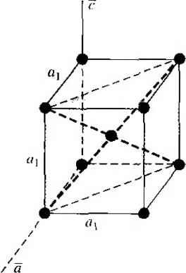 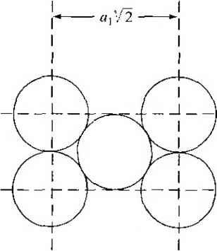 Figure 1,8 I (a) The (110) plane in a body-centered cubic and (b) the atoms cut by the (110) plane in a body-centered cubic. Solution We find the surface density by dividing the number of lattice atoms by the surface area, or in this case Surface density = 2 atoms (А,)( ,л/2) (5x 10-)(л/2) which is 5.66 X lO * atoms/cm~ Comment The surface density of atoms is a function of the particular crystal plane in the lattice and gen erally varies from one crystal plane to another. TEST YOUR UNDERSTANDING E1.3 Determine the distance between nearest (110) planes iti a simple cubic lattice with a lattice constant of an = 4.83 A. (VZV£ *suv) о El.4 The lattice constant of a face-centered-cubic structure is 4.75 A. Calculate the surface density of atoms for (a) a (100) plane and (i?) a (110) plane. U- riOI X 1Г9 (q) hOI X 988 suy] In addition to describing crystal planes in a lattice, we may want to describe a particular direction in the crystal. The direction can be expressed as a set of three integers which are the components of a vector in that direction. For example, the body diagonal in a simple cubic lattice is composed of vector components 1, 1, 1. The body diagonal is then described as the [1111 direction. The brackets are used to designate direction as distinct from the parentheses used for the crystal planes. The three basic directions and the associated crystal planes for the siinple cubic structure are shown in Figure 1.9. Note that in the simple cubic lattices, the [hkl] direction is perpendicular to the (hkl) plane. This perpendicularity may not be true in noncubic lattices. 13.4 The Diamond Structure As already stated, silicon is the most common semiconductor material. Silicon is referred to as a group IV element and has a diamond crystal structure. Germanium is also a group IV element and has the same diamond structure. A unit cell of the diamond structure, shown in Figure 1.10, is more complicated than the simple cubic structures that we have considered up to this point. We may begin to understand the diamond lattice by considering the tetrahedral structure shown in Figure 1.11. This structure is basically a body-centered cubic with 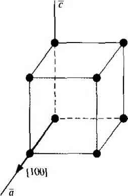 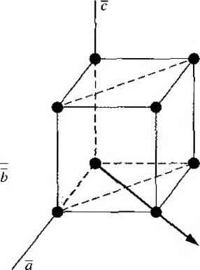 [UOl 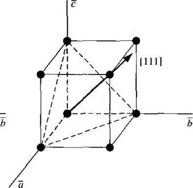 Figure 1.9 I Three lattice directions and planes: (a) (100) plane and llOOj direction, (b) (110) plane and fl 101 direction, (c)(ИI)plane and[\\\] direction. 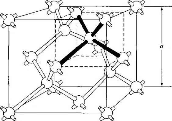 Figure 1.10 I The diamond structure. Figure 1.111 The tetrahedral structure of closest neighbors in the diamond lattice. 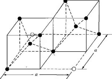 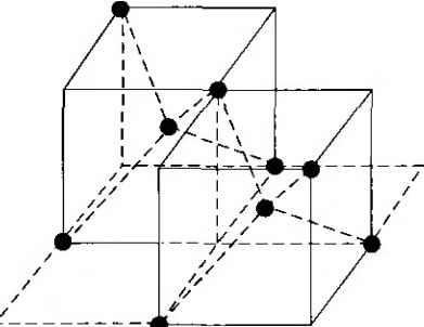 (a) (b) Figure 1.12 I Portions of the diamond lattice: (a) bottom half and (b) top half. four of the comer atoms missing. Every atom in the tetrahedral structure has four nearest neighbors and it is this structure which is the basic building block of the diamond lattice. There are several ways to visualize the diamond structure. One way to gain a further understanding of the diamond lattice is by considering Eigure t. 12. Eigure 1.12a shows two body-centered cubic, or tetrahedral, structures diagonally adjacent to each other. The shaded circles represent atoms in the lattice that are generated when the structure is translated to the right or left, one lattice constant, a. Eigure 1.12b represents the top half of the diamond structure. The top half again consists of two tetrahedral structures joined diagonally, but which are at 90 with respect to the bottom-half diagonal. An important characteristic of the diamond lattice is that any atom within the diamond structure will have four nearest neighboring atoms. We will note this characteristic again in our discussion of atomic bonding in the next section. 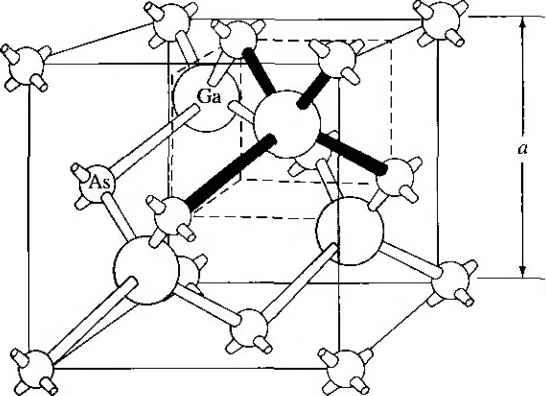 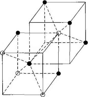 Figure 1.13 I The zincblende (sphalerite) lattice of GaAs. Figure 1.14 I The tetrahedral structure of closest neighbors in the zincblende lattice. The diamond structure refers to the particular lattice in which all atoms are of the same species, such as silicon or germanium. The zincblende (sphalerite) structure differs from the diamond structure only in that there are two different types of atoms in the lattice. Compound semiconductors, such as gallium arsenide, have the zincblende structure shown in Figure 1.13. The important feature of both the diamond and the zincblende structures is that the atoms are joined together to form a tetrahedron. Figure 1.14 shows the basic tetrahedral structure of GaAs in which each Ga atom has four nearest As neighbors and each As atom has four nearest Ga neighbors. This figure also begins to show the interpcnctration of two sublattices that can be used to generate the diamond or zincblende lattice. TEST YOUR UNDERSTANDING El.5 The lattice constant of silicon is 5.43 A. Calculate the volume density of silicon atoms. (е шэ .qi xg suy) 1.4 I ATOMIC BONDING We have been considering various single-crystal structures. The question arises as to why one particular crystal structure is favored over another for a particular assembly of atoms. A fundamental law of nature is that the total energy of a system in thermal equilibrium tends to reach a minimum value. The interaction that occurs between atoms to form a solid and to reach the minimum total energy depends on the type of atom or atoms involved. The type of bond, or interaction, between atoms, then, depends on the particular atom or atoms in the crystal. If there is not a strong bond between atoms, they will not stick together to create a solid. The interaction between atoms can be described by quantum mechanics. Although an introduction to quantum mechanics is presented in the next chapter, the quantum-mechanical description of the atomic bonding interaction is still beyond the scope of this text. We can nevertheless obtain a qualitative understanding of how various atoms interact by considering the valence, or outermost, electrons of an atom. The atoms at the two extremes of the periodic table (excepting the inert elements) tend to lose or gain valence electrons, thus forming ions. These ions then essentially have complete outer energy shells. The elements in group i of the periodic table tend to lose their one electron and become positively charged, while the elements in group Vll tend to gain an electron and become negatively charged. These oppositely charged ions then experience a coulomb attraction and form a bond referred to as an ionic bond. Tf the ions were to get too close, a repulsive force would become dominant, so an equilibrium distance results between these two ions. In a crystal, negatively charged ions tend to be surrounded by positively charged ions and positively charged ions tend to be surrounded by negatively charged ions, so a periodic array of the atoms is formed to create the lattice. A classic example of ionic bonding is sodium chloride. The interaction of atoms tends to form closed valence shells such as we see in ionic bonding. Another atomic bond that tends to achieve closed-valence energy shells is covalent bonding, an example of which is found in the hydrogen molecule. A hydrogen atom has one electron and needs one more electron to complete the lowest energy shell. A schematic of two noninteracting hydrogen atoms, and the hydrogen molecule with the covalent bonding, are shown in Figure 1Л5. Covalent bonding results in electrons being shared between atoms, so that in effect the valence energy shell of each atom is full. Atoms in group IV of the periodic table, such as silicon and germanium, also tend to form covalent bonds. Each of these elements has four valence electrons and needs four more electrons to complete the valence energy shell. If a silicon atom, for example, has four nearest neighbors, with each neighbor atom contributing one valence electron to be shared, then the center atom will in effect have eight electrons in its outer shell. Eigure 1Л6а schematically shows five noninteracting silicon atoms with the four valence electrons around each atom. A two-dinnensional representation H- -Гн H}=(H (b) Figure 1Л5 [ Representation of (a) hydrogen valence electrons and (b) covalent bonding in a hydrogen molecule. Sj)-I -(Si I -(Si)- I [l I -(§)-(§)=(si I II Figure 1Л61 Representation of (a) silicon valence electrons and (b) covalent bonding in the silicon crystal. of the covalent bonding in silicon is shown in Figure 1Л 6b. The center atom has eight shared valence electrons. A significant difference between the covalent bonding of hydrogen and of silicon is that, when the hydrogen molecule is formed, it has no additional electrons to form additional covalent bonds, while the outer silicon atoms always have valence electrons available for additional covalent bonding. The silicon array may then be formed into an infinite crystal, with each silicon atom having four nearest neighbors and eight shared electrons. The four nearest neighbors in silicon forming the covalent bond correspond to the tetrahedral structure and the diamond lattice, which were shown in Figures 1.11 and 1.10, respectively. Atomic bonding and crystal structure are obviously directly related. The third major atomic bonding scheme is referred to as metallic bonding. Group I elements have one valence electron. If two sodium atoms (Z - 11), for example, are brought into close proximity, the valence electrons interact in a way similar to that in covalent bonding. When a third sodium atom is brought into close proximity with the first two, the valence electrons can also interact and continue to form a bond. Solid sodium has a body-centered cubic structure, so each atom has eight nearest neighbors with each atom sharing many valence electrons. We may think of the positive metallic ions as being surrounded by a sea of negative electrons, the solid being held together by the electrostatic forces. This description gives a qualitative picture of the metallic bond. A fourth type of atomic bond, called the Van der Waals bond, is the weakest of the chemical bonds. A hydrogen fluoride (HF) molecule, for example, is formed by an ionic bond. The effective center of the positive charge of the molecule is not the same as the effective center of the negative charge. This nonsymmetry in the charge distribution results in a small electric dipole that can interact with the dipoles of other HF molecules. With these weak interactions, solids formed by the Van der Waals bonds have a relatively low melting temperature-in fact, most of these materials are in gaseous form at room temperature. Ч.5 I IMPERFECTIONS AND IMPURITIES IN SOLIDS Up to this point, we have been considering an ideal single-crystal structure. In a real crystal, the lattice is not perfect, but contains imperfections or defects; that is, the perfect geometric periodicity is disrupted in some manner. Imperfections tend to alter the electrical properties of a material and, in some cases, electrical parameters can be dominated by these defects or impurities. 1,5Л Imperfections in Solids One type of imperfection that all crystals have in common is atomic thermal vibration. A perfect single crystal contains att)ms at particular lattice sites, the atoms separated from each other by a distance we have assumed to be constant. The atoms in a ♦Indicates sections that can be skipped without loss of continuity. (a) (b) Figure 1Л7 I Two-dimensional representation of a single-crystal lattice showing (a) a vacancy defect and (b) an interstitial defect. crystal, however, have a certain thermal energy, which is a function of temperature. The thermal energy causes the atoms to vibrate in a random manner about an equilibrium lattice point. This random thermal motion causes the distance between atoms to randomly fluctuate, slightly disrupting the perfect geometric arrangement of atoms. This imperfection, called lattice vibrations, affects some electrical parameters, as we will see later in our discussion of semiconductor material characteristics. Another type of defect is called a point defect. There are several of this type that we need to consider. Again, in an ideal single-crystal lattice, the atoms are arranged in a perfect periodic arrangement. However, in a real crystal, an atom may be missing from a particular lattice site. This defect is referred to as a vacancy; it is schematically shown in Figure L17a. In another situation, an atom may be located between lattice sites. This defect is referred to as an interstitial and is schematically shown in Figure 1.17b. In the case of vacancy and interstitial defects, not only is the perfect geometric arrangement of atoms broken, but also the ideal chemical bonding between atoms is disrupted, which tends to change the electrical properties of the material. A vacancy and interstitial may be in close enough proximity to exhibit an interaction between the two point defects. This vacancy-interstitial defect, also known as a Frenkel defect, produces different effects than the simple vacancy or interstitial. The point defects involve single atoms or single-atom locations. In forming single-crystal materials, more complex defects may occur. A line defect, for example, occurs when an entire row of atoms is missing from its nonnal lattice site. This defect is referred to as a line dislocation and is shown in Figure 1.18. As with a point defect, a line dislocation disrupts both the normal geometric periodicity of the lattice and the ideal atomic bonds in the crystal. This dislocation can also alter the electrical properties of the material, usually in a more unpredictable manner than the simple point defects. Other complex dislocations can also occur in a crystal lattice. However this introductory discussion is intended only to present a few of the basic types of defect, and to show that a real crystal is not necessarily a perfect lattice structure. The effect of these imperfections on the electrical properties of a semiconductor will be considered in later chapters. I I I I T T T till ! I T T + \ i i I I 1 I \ + t + i t I f J 1 1 Figure 1.18 I A two-dimensional representation of a line dislocation.  Substitutional impurity / / / / / / / / / / / / / / / Interstitial 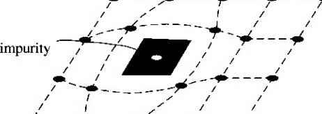 Figure 1.19 I Two-dimensional representation of a single-crystal lattice showing (a) a substitutional impurity and (b) an intersitital impurity. 1.5,2 Impurities in Solids Foreign atoms, or impurity atoms, may be present in a crystal lattice. Impurity atoms may be located at normal lattice sites, in which case they are called substitutional impurities. Impurity atoms may also be located between normal sites, in which case they are called interstitial impurities. Both these impurities are lattice defects and are schematically shown in Figure 1.19. Some impurities, such as oxygen in silicon, tend to be essendally inert; however, other impurities, such as gold or phosphorus in silicon, can drastically alter the electrical properties of the material. In Chapter 4 we will see that, by adding controlled amounts of particular impurity atoms, the electrical characteristics of a semiconductor material can be favorably altered. The technique of adding impurity atoms to a semiconductor material in order to change its conductivity is called doping. There are two general methods of doping: impurity diffusion and ion implantation. The actual diffusion process depends to some extent on the material but, in general, impurity diffusion occurs when a semiconductor crystal is placed in a high-temperature lOOOC) gaseous atmosphere containing the desired impurity atom. At this high temperature, many of the crystal atoms can randomly move in and out of their single-crystal lattice sites. Vacancies may be created by this random motion so that impurity atoms can move through the lattice by hopping from one vacancy to another. Impurity diffusion is the process by which impurity particles move from a region of high concentration near the surface, to a region of lower concentration within the crystal. When the temperature decreases, the impurity atoms become permanently frozen into the substitutional lattice sites. Diffusion of various impurities into selected regions of a semiconductor allows us to fabricate complex electronic circuits in a single semiconductor crystal. Ion implantation generally takes place at a lower temperature than diffusion. A beam of impurity ions is accelerated to kinetic energies in the range of 50 keV or greater and then directed to the surface of the semiconductor. The high-energy impurity ions enter the crystal and come to rest at some average depth from the surface. One advantage of ion implantation is that controlled numbers of impurity atoms can be introduced into specific regions of the crystal. A disadvantage of this technique is that the incident impurity atoms collide with the crystal atoms, causing lattice-displacement damage. However, most of the lattice damage can be removed by thermal annealing, in which the temperature of the crystal is raised for a short time. Thermal annealing is a required step after implantation. *1.6 I GROWTH OF SEMICONDUCTOR MATERIALS The success in fabricating very large scale integrated (VLSI) circuits is a result, to a large extent, of the development of and improvement in the formation or growth of pure single-crystal semiconductor materials. Semiconductors are some of the purest materials. Silicon, for example, has concentrations of most impurities of less than 1 part in 10 billion. The high purity requirement means that extreme care is necessary in the growth and the treatment of the material at each step of the fabrication process. The mechanics and kinetics of crystal growth are extremely complex and will be described in only very general terms in this text. However, a general knowledge of the growth techniques and terminology is valuable. 1.6Л Growth from a Melt A common technique for growing single-crystal materials is called the Czochraiski method. In this technique, a small piece of single-crystal material, known as a seed, is brought into contact with the surface of the same material in liquid phase, and then slowly pulled from the melt. As the seed is slowly pulled, solidification occurs along the plane between the solid-liquid interface. Usually the crystal is also rotated slowly as it is being pulled, to provide a slight stirring action to the melt, resulting in a more uniform temperature. Controlled amounts of specific impurity atoms, such as boron or phosphorus, may be added to the melt so that the grown semiconductor crystal is intentionally doped with the impurity atom. Figure 1.20 shows a schematic of the Czochraiski growth process and a silicon ingot or boule grown by this process. Indicates sections that can be skipped without loss of continuity. Chuck Seed Crystal  Heaters Container О О о о о е о Tube Мек Crucible  Figure 1.201 (а) Model of а crystal puller and (b) photograph of a silicon wafer with an array of integrated circuits. The circuits are tested on the wafer then sawed apart into chips that are mounted into packages, (Photo courtesy of Intel Софога11оп.) 1 2 3 4 5 ... 55 |
|
© 2026 AutoElektrix.ru
Частичное копирование материалов разрешено при условии активной ссылки |