 |
 |
 |
| Главная Журналы Популярное Audi - почему их так назвали? Как появилась марка Bmw? Откуда появился Lexus? Достижения и устремления Mercedes-Benz Первые модели Chevrolet Электромобиль Nissan Leaf |
Главная » Журналы » Absorbing materialorganic polymer 1 ... 19 20 21 22 23 24 25 ... 55 dp(x, t) jc = 0 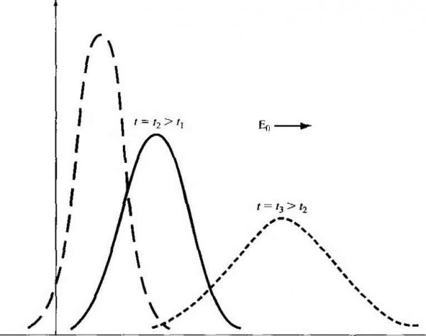 Distance, X Figure 6.9 i Excess-hole concentration versus distance at various times for a constant applied electric held. with the excess electrons so that at f = oo the excess hole concentration is zero. In this particular example, both diffusion and recombination processes are occurring at the same time. Figure 6.9 shows a plot of Equation (6.70) as a function of distance x at various times for the case when the applied electric field is not zero. In this case, the pulse of excess minority carrier holes is drifting in the -\-x direction, which is the direction of the electric field. We still have the same diffusion and recombination processes as we had before. An important point to consider is that, with charge neutrality, Su - SpuX any instant of time and at any point in space. The excess-electron concentration is equal to the excess-hole concentration. In this case, then, the excess-electron pulse is moving in the same direction as the applied electric field even though the electrons have a negative charge. In the ambipolar transport process, the excess carriers are characterized by the minority carrier parameters. In this example, the excess carriers behave according to the minority carrier hole parameters, which include Dp, p, and TpQ. The excess majority carrier electrons are being pulled along by the excess minority carrier holes. TEST YOUR UNDERSTANDING E6.7 As a good approximation, the peak value of a normalized excess carrier concentration, given by Equafion (6.70), occurs aix = ppEot, Assume the following parameters: TpQ 5 /xs. Dp = 10 cm/s, Др = 386 cm/V-s, and Eq - 10 V/cm. Calculate the peak value at times of {o)t = 1 /xs, {h)t 5 /xs, (c) т = 15 Д8, and () r = 25 /xs. What are the corresponding values of jc for parts {a) to f £96 = *0l 0 (Я) E6.8 The excess carrier concentration, given by Equation (6 JO), is to be calculated at distances of one diffusion length away from the peak value. Using the parameters given in E6.7, calculate the values ofSp for (й) / = 1 psat U) 1.093 x 10- cm and iii)x = -3.21 X 10- cm; ib)t =5 ms at (0 x = 2.64 x 10 cm and (ii) X = 1.22 X 10~ cm; (c) r = 15 /xs at ii)x = 6.50 x 10 - cin and 07) .V = 5.08 X 10- cm. [eOT (..0 gOT (.0 P) tTI (.0 Vll (.0 {Я) -вЖ (/.0 бОг (.0 Н suvl Еб.9 Using the parameters given in E6.7, (a) plot Sp(x,f) from Equation (6.70) versus x for (i)t 1 /xs, {ii) t - 5 fis, and (Hi) t = 15 s, and {b) plot Sp{x. t) versus time for {i)x = 10 cm, iii)x 3 x 10 cm, and (Hi) .v 6 x 10 ctn.  6.3.4 Dielectric Relaxation Time Constant We have assumed in the previous analysis that a quasi-neutrality conditions exists- that is, the concentration of excess holes is balanced by an equal concentration of excess electrons. Suppose that we have a situation as shown in Figure 6.10, in which a uniform concentration of holes Sp is suddenly injected into a portion of the surface of a semiconductor. We will instantly have a concentration of excess holes and a net positive charge density that is not balanced by a concentration of excess electrons. How is charge neutrality achieved and how fast? There are three defining equations to be considered. Poissons equation is (6.71) The current equation. Ohms law, is I J =aE (6,72) The continuity equation, neglecting the effects of generation and recombination, is Эр St (6.73) holes  Figure 6Л01 The injection of a concentration of holes into a small region at the surface of an n-type semwonductor. Substituting Equation (6.74) into the continuity equation, we have op dp dp (6.75) Since Equation (6.75) is a function of time only, we can write the equation as a total derivative. Equation (6.75) can be rearranged as + I-!p = o (6.76) Equauon (6.76) is a first-order differential equation whose solution is pit) p{0)e- (6.77) where Td = - (6.78) and is called the dielectric relaxation time constant EXAMPLE 6,5 Objecrive Calculate the dielectric relaxation time constant for a particular semiconductor. Assume an n-type semiconductor with a donor impurity concentration of Nj = 10 cm Solution The conductivity is found as о eii N = (1.6 X 10-)(1200)00) = 1.92 (П-ст) where the value of mobility is the approximate value found from Figure 53. The permittivity of silicon is € = = (11.7)(8.85 X 10-) F/cm The dielectric relaxation time constant is then € (11.7)(8.85x 10-) - =----= 5.39 X 10 s a 1.92 = 0.539 ps The parameter f> is the net charge density and the initial value is given by е{Ьр). We will assume that bp is uniform over a short distance at the surface. The parameter e is the permittivity of the semiconductor. Taking the divergence of Ohms law and using Poissons equation, we find V J = aV-E- (6.74) Comment Equation (6.77) then predicts that in approximately four time constants, or in approximately 2 ps, the net charge density is essentially zero; that is, quasi-neutrahty has been achieved. Since the continuity equation, Equation (6.73), does not contain any generation or recombination terms, the initial positive charge is then neutralized by pulling in electrons from the bulk n-type material to create excess elecU-ons. This process occurs very quickly compared to the normal excess carrier lifetimes of approximately 0Л /is. The condition of quasi-charge-neutral ity is then justified. *6.3.5 Haynes-Shockley Experiment We have derived the mathematics describing the behavior of excess carriers in a semiconductor. The Haynes-Shockley experiment was one of the first experiments to actually measure excess-carrier behavior. Figure 6.11 shows the basic experimental arrangement. The voltage source Vi establishes an applied electric field Eq in the -fx direction in the n-type semiconductor sample. Excess carriers are effecrively injected into the semiconductor at contact A. Contact В is a recrifying contact that is under reverse bias by the voltage source V2- The contact В will collect a fraction of the excess carriers as they drift through the semiconductor. The collected carriers will generate an output voltage, Vq. This experiment corresponds to the problem we discussed in Example 6.4. Figure 6.12 shows the excess-carrier concentrations at contacts A and В for two conditions. Figure 6Л2а shows the idealized excess-carrier pulse at contact A at time / = 0. For a given electric field Eoi, the excess carriers will drift along the semiconductor producing an output voltage as a function of time given in Figure 6.12b. The peak of the pulse will arrive at contact В at time /{j. If the applied electric field is reduced to a value E02, E02 < Eoi, the output voltage response at contact В will look approximately as shown in Figure 6.12c. For the smaller electric field, the drift velocity of the pulse of excess carriers is smaller, and so it will take a longer lime for the 1- Vi 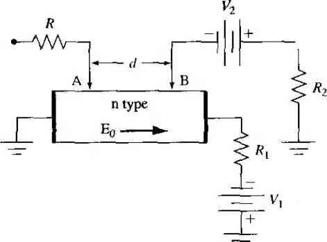 Figure 6Л11 The basic Haynes-Shockley experimental arrangement. о с Time 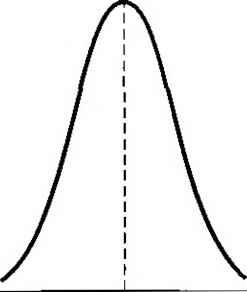 Electric field. Ei Time \ Electric field, \ Ч Time Figure 6.12 I (a) The idealized excess-carrier pulse at terminal A at Г = 0, (b) The excess-carrier pulse versus time at terminal В for a given applied electric field, (c) The excess-carrier pulse versus time at terminal В for a smaller applied electric field. pulse to reach the contact B. During this longer time period, there is more diffusion and more recombination. The excess-carrier pulse shapes shown in Figures 6Л 2b and 6.12c are different for the two electric field conditions. The minority carrier mobility, liferime, and diffusion coefficient can be deter mined from this single experiment. As a good first approximation, the peak of the minority carrier pulse will arrive at contact В when the exponent involving distance and time in Equation (6.70) is zero, or X - fiphot = 0 (6.79a) In this case x = d, where d is the distance between contacts A and B, and t = to, where to is the time at which the peak of the pulse reaches contact B. The mobility may be calculated as (6.79b) Figure 6.13 again shows the output response as a function of time. At times ti and the magnitude of the excess concentration is of its peak value, if the time difference between ti and t2 is not too large, e* and (47гD,0 do not change appreciably during this time; then the equation (d - fipEoty (6.80) is satisfied at both t = ti and r = f2- If we set t = fj and / = /2 in Equation (6.80) and add the two resulting equations, we may show that the diffusion coefficient is given by Dp = (fipEo)HAty 16fo (6.81) where At = t2- tl (6.82) 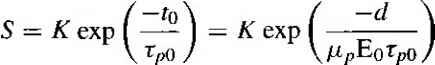 The area S under the curve shown in Figure 6ЛЗ is proportional to the number of excess holes that have not recombined with majority carrier electrons. We may write (6.83) where К is г. constant. By varying the electric field, the area under the curve will change. A plot of In (5) as a function of {d/PpEo) will yield a straight line whose slope is (l/Tpo), so the minority carrier lifetime can also be determined from this experiment. The Haynes-Shockley experiment is elegant in the sense that the three basic processes of drift, diffusion, and recombination are all observed in a single experiment. 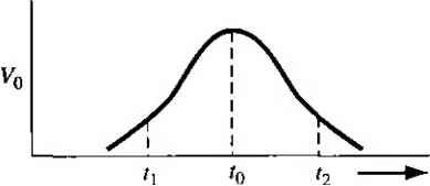 Time Figure 6ЛЗ I The output excess-carrier pulse versus time to determine the diffusion coefficient. The determination of mobility is straightforward and can yield accurate values. The determination of the diffusion coefficient and lifetime is more complicated and may i lead to some inaccuracies. 6.4 I QUASI-FERMI ENERGY LEVELS The thermal-equilibrium electron and hole concentrations are functions of the Fermi energy level. We can write (Ef - Efi\ (6.84a) Po = n, exp I - I (6.84b) where Ef and Efj are the Fermi energy and intrinsic Fermi energy, respectively, and Hi is the intrinsic carrier concentration. Figure 6.14a shows the energy-band diagram for an n-type semiconductor in which Ep > Efi. For this case, we may note from Equations (6.84a) and (6.84b) that fiQ > and < as we would expect. Similarly, Figure 6.14b shows the energy-band diagram for a p-type semiconductor in which Ef < Efi. Again we may note from Equations (6.84a) and (6.84b) that 0 < and po > ni, as we would expect for the p-type material. These results are for thermal equilibrium. If excess carriers are created in a semiconductor, we are no longer in thermal equilibrium and the Fermi energy is strictly no longer defined. However, we may define a quasi-Fermi level for electrons and a quasi-Fermi level for holes that apply for nonequilibrium. If Sn and Sp are the excess electron and hole concentrations, respectively, we may write: , / Ffn - Efi no -hSn = n, exp I-~- (6.85a) с о Л (И Щ Figure 6Л4 I Thcnmal-equilibrium energy-band diagrams for {a) n-type semiconductor and (6> p-type semiconductor. 6 - 4 Quasi-Ferml Energy Levels 217  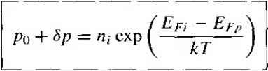 (6.85b) where f/r and Efp are the quasi-Perm j energy levels for electrons and holes, respectively. The total electron concentration and the total hole concentration are functions of the quasi-Fermi levels. Objective example 6.6 To calculate the quasi-Fermi energy levels. Consider an n-type semiconductor at Г = 300 К with carrier concentrations of - 10* cm -. Hi = 10 cm-*, and po = cm~. In nonequilibrium, assume that the excess carrier concentrations are 6 = 5p 10 * cm-\ Solution The Fermi level for thermal equiUbriuin can be determined from Equation (6.84a). We have Er - Efi = kT In -j 0,2982 eV We can use Equation (6.85a) to determine the quasi-Fermi level for electrons in nonequilibrium. We can write Ef, - Efi кТ\п {- 2984 eV Equation (6.85b) can be used to calculate the quasi-Fermi level for holes in nonequilibrium. We can write 1 Efi - Etjy = kT In ( = 0.179 eV Comment We may note that the quasi-Fermi level for electrons is above En while the quasi-Fermi level for holes is below Е/.,. Figure 6.15a shows the energy-band diagram with the Fermi energy level corresponding to thermal equilibrium. Figure 6.15b now shows the energy-band diagram under the nonequilibrium condition. Since the majority carrier electron concentration does not change significantly for this low-injection condition, the quasi-Fermi level for electrons is not much different from the thermal-equilibrium Fermi level. The quasi-Fermi energy level for the minority carrier holes is significanriy different from the Fermi level and illustrates the fact that we have deviated from thermal equilibrium significanriy. Since the electron concentrarion has increased, the quasi-Fermi level for electrons has moved slightly closer to the conduction band. The hole 0.2982 eV 0.2982 eV с
Figure 6.15 1 (a) Thermal-equilibriura energy-band diagram for = 10 cm and . (b) Quasi-Fermi levels for electrons and holes if lO cm excess hi = 10 cm carriers are present. concentration has increased significantly so that the quasi-Fermi level for holes has moved much closer to the valence band. We will consider the quasi-Fermi energy levels again when we discuss forward-biased pn junctions. TEST YOUR UNDERSTANDING E6.10 Silicon aiT - 300 К is doped at impurity concentrations of Л^ = 10 cm- and = 0. Excess carriers are generated such that the steady-state values are Sn = Sp - 5 x W cm~-\ (a) Calculate the thermal equilibrium Fermi level with respect io Efi, (b) Determine Ef and Efp with respect to Efi. lA A693*0 - - -.7 4 98K0 - - 3 (Я) -ЛЭ ШГО = -3 - 3 Н suy] E6.11 Impurity concentrations of = 10 cm and ~6 x 10 * cm are added to silicon at Г = 300 К. Excess carriers are generated in the material such that the steady-state concentrations are 6/7 = 2 x 10 * cm. (a) Find the thermal equilibrium Fermi level with respect to Ef/. (b) Calculate Ef and Efp with respect to Efi, [ЛЭ toeeo = - -3 a 09fto = - -я № A t6£-0 = - 3 W -suvl 6.5 I EXCESS-CARRIER LIFETIME The rate at which excess electrons and holes recombine is an important characteristic of the semiconductor and influences many of the device characteristics, as we will see in later chapters. We considered recombination briefly at the beginning of this chapter and argued that the recombination rate is inversely proportional to the mean carrier lifetime. We have assumed up to this point that the mean carrier liferime is simply a parameter of the semiconductor material. We have been considering an ideal semiconductor in which electronic energy states do not exist within the forbidden-energy bandgap. This ideal effect is present in a perfect single-crystal material with an ideal periodic-potential function. In a real semiconductor material, defects occur within the crystal and disrupt the perfect periodic-potential function. If the density of these defects is not too great, the defects will create discrete electronic energy states within the forbidden-energy band. These allowed energy states may be the dominant effect in determining the mean carrier lifetime. The mean carrier lifetime may be determined from the Shockley-Read-Hall theory of recombination. 6.5.1 Shockley-Read-Hall Theory of Recombination An allowed energy state, also called a trap, within the forbidden bandgap may act as a recombination center, capturing both electrons and holes with almost equal probability. This equal probability of capture means that the capture cross sections for electrons and holes are approximately equal. The Shockley-Read-Hall theory of recombinarion assumes that a single recombination center, or trap, exists at an energy Ef within the bandgap. There are four basic processes, shown in Figure 6.16, that may occur at this single trap. We will assume that the trap is an acceptor-type trap; that is, it is negatively charged when it contains an electron and is neutral when it does not contain an electron. The four basic processes are as follows: Process 1: The capture of an electron from the conduction band by an inirially neutral empty trap. Process 1 Process 2 EJeciron capture Elccrroj] emission Process 3 Process 4 Hole capture Hole emission Figure 6.161 The four basic trapping and emission processes for the case of an acceptor-type trap. 1 ... 19 20 21 22 23 24 25 ... 55 |
||||||||||||||
|
© 2026 AutoElektrix.ru
Частичное копирование материалов разрешено при условии активной ссылки |