 |
 |
 |
| Главная Журналы Популярное Audi - почему их так назвали? Как появилась марка Bmw? Откуда появился Lexus? Достижения и устремления Mercedes-Benz Первые модели Chevrolet Электромобиль Nissan Leaf |
Главная » Журналы » Absorbing materialorganic polymer 1 ... 21 22 23 24 25 26 27 ... 55 quasi-Fermi level The quasi-Fermi level for electrons and the quasi-Fermi level for holes relate the nonequilibrium electron and hole concentrations, respectively, to the intrinsic carrier concentration and the intrinsic Fenui level. recombination rate The rate (#/cm-s) at which electron-hole pairs recombine. surface recombination velocity A parameter that relates the gradient of the excess carrier concentration at a surface to the surface concentration of excess carriers, surface states The electronic energy states that exist within the bandgap at a semiconductor surface. CHECKPOINT After studying this chapter, the reader should have the ability to: Describe the concept of excess generation and recombination. Describe the concept of an excess carrier lifetime. Describe how the time-dependent diffusion equations for holes and electrons are derived. Describe how the ambipolar transport equation is derived. Understand the consequence of the coefficients in the ambipolar transport equation reducing to the minority carrier values under low injection and extrinsic semiconductors. Apply the ambipolar transport equation to various problems. Understand the concept of the dielectric relaxation time constant. Calculate the quasi-Fermi levels for electrons and holes. Calculate the excess carrier recombination rate for a given concentration of excess carriers. Understand the effect of a surface on the excess carrier concentrations. REVIEW QUESTIONS 1. Why are the electron generation rate and recombination rate equal in thermal equilibrium? 2. Explain how the density of holes, for example, can change as a result of a change in the flux of particles. 3. Why is the general ambipolar transport equation nonlinear? 4. Explain qualitatively why a pulse of excess electrons and holes would move together in the presence of an applied electric field. 5. Explain qualitatively why the excess carrier lifetime reduces to that of the minority carrier under low injection. 6. What is the time dependence of the density of excess carriers when the generation rate becomes zero? 7. In the presence of an external force, why doesnt the density of excess carriers continue to increase with time? 8. When a concentration of one type of excess carrier is suddenly created in a semiconductor, what is the mechanism by which the net charge density quickly becomes zero? 9- State the definition of the quasi-Fermi level for electrons. Repeat for holes. 10. Why, in general, is the concentration of excess carriers less at the surface of a semiconductor than in the bulk? Problems 231 PROBLEMS {Note: Use the semiconductor parameters listed in Appendix В if they are not speciiically given in a problem. Assume T = 300 K.) Section 6.1 Carrier Generation and Recombination 6.1 Consider a semiconductor in which л о = 10 cm * and = 10 cm~-. Assume that the excess-carrier lifetime is 10~ s. Determine the electron-hole recombination rate if the excess-hole concentration isSp = 5 x JO cm~\ 6.2 A semiconductor, in thermal equilibrium, has a hole concentration of pQ = 10 cm and an intrinsic concentration of n, - 10 cm~\ The minority carrier lifetime is 2 X 10 s. (a) Determine the thermal-equilibrium recombination rate of electrons. (h) Determine the change in the recotnbination rate of electrons if an excess electron concentration of (Sfi = 10- cm exists. 6.3 An n-type silicon sample contains a donor concentration of Nj = 10 cm~-. The minority carrier hole lifetime is found to be Тро = 20 jus. (a) What is the lifetime of the majority carrier electrons? {h) Determine the thermal equilibrium generation rate for electrons and holes in this material, (c) Determine the thermal equilibrium recombination rate for electrons and holes in this material. 6.4 (a) A sample of semiconductor has a cross-sectionaJ area of I cm and a thickness of 0Л cm. Determine the number of electron-hole pairs that are generated per unit volume per unit time by the uniform absoфtion of I watt of light at a wavelength of о 6300 A. Assume each photon creates one electron-hole pair, {h) If the excess minority carrier lifetime is 10 s. what is the steady-state excess carrier concentration? Section 6.2 Mathematical Analysis of Excess Carriers 6.5 Derive Equation (6.27) from Equations (6.18) and (6.20). 6.6 Consider a one-dimensional hole flux as shown in Figure 6.4. If the generation rate of holes in this differential volume is gp = 10- cm -s and the recombination rate is 2 X 10 cm-s , what must be the gradient in the particle current density to maintain a steady-state hole concentration? 6.7 Repeat Problem 6.6 if the generation rate becomes zero. Section 6.3 Ambipolar Transport 6.8 Starting with the continuity equations given by Equations (6.29) and (6.30), derive the ambipolar transport equation given by Equation (6.39). 6.9 A sample of Ge at T = 300 К has a uniform donor concentration of 2 x 10- cm~. The excess carrier lifetime is found to be Zpo = 24 /zs. Determine the ambipolar diffusion coefficient and the ambipolar mobility. What are the electron and hole lifetimes? 6.10 Assume that an n-type semiconductor is uniformly illuminated, producing a uniform excess generation rate g\ Show that in steady state the change in the semiconductor conductivity is given by Да = e{p, +Pp)Tpog 6.11 Light is incident on a sihcon sample starting at / = 0 and generating excess carriers uniformly throughout the silicon for r > 0. The generation rate is g = 5 x 102 cm-- s-. The silicon {T = 300 K) is n type with N,i = 5 x 10 cm and Na = 0. Let rt, = 1.5 X 10 cm-\ r o = 10 s, and ro = 10 s. Also let д„ = 1000 cm-/V-s and Pp = 420 cmA-s. Determine the conductivity of the silicon as a function of time for r > 0. 6.12 An n-type gallium arsenide semiconductor is doped with Nj = lO cm- * and Na =0. The minority carrier lifetime is rJO = 2 x 10 s. Calculate the steady-state increase in conductivity and the steady-state excess carrier recombination rate if a uniform generation rate, g = 2 x 10 cm--s , is incident on the semiconductor. 6.13 A sihcon sample at Г = 300 К is n type with Л^ =5 x 10 cm - and Na = 0. The sample has a length of 0,1 cm and a cross-secdonal area of 10 cm. A voltage of 5 V is applied between the ends of the sample. For Г < 0, the sample has been illuminated with light, producing an excess-carrier generation rate of = 5 x 10 cm -s uniformly throughout the entire silicon. The minority carrier lifetime is ro =3 X iO~ s. At = 0, the light is turned off Derive the expression for the current in the sample as a function of time r > 0. (Neglect surface effects.) 6Л4 Consider a homogeneous gallium arsenide semiconductor at Г = 300 К with yv = 10 cm and Nj = 0. A light source is turned on at f = 0 producing a uniform generation rate of g = 10 cm-s~. The electric field is zero, (a) Derive the expression for the excess-carrier concentration and excess carrier recombination rate as a function of time, (b) If the maximum, steady-state, excess-carrier concentradon is to be 1 X 10 cm , determine the maximum value of the minority carrier lifetime. (c) Determine the times at which the excess minority carrier concentration will be equal to (г) three-fourths, (ii) one-half, and ( /) one-fourth of the steady-state value. 6.15 In a sihcon semiconductor material at Г = 300 К, the doping concentrations are Nj = 10 cm - and N = 0. The equilibrium recombination rate is ?,o = 10 cm--s- A uniform generation rate produces an excess-carrier concentration of 5n = Sp 10* cm -, (a) By what factor does the total recombination rate increase? {h) What is the excess-carrier lifetime? 6.16 Consider a silicon material doped with 3 x lO* cm donor atoms. At f = 0, a light source is turned on, producing a uniform generation rate of = 2 x lO** cm-s . At / = 10 s, the light source is turned off Determine the excess minority carrier concentration as a function of Г for 0 < Г < oo. Let т^,o = 10 s. Plot the excess minority carrier concentration as a function of time. 6.17 A semiconductor has the following properties: D = 25 cmVs r a = 10 s Dp = 10 curls Tpii = 10 s The semiconductor is a homogeneous, p-type {N = 10 cm -) material in thermal equilibrium for / < 0. At f 0, an external source is turned on which produces excess carriers uniformly at the rate of g = 10 cm-s . At Г = 2 x Ю * s, the external source is turned off. (a) Derive the expression for the excess-electron concentration as a function of time for 0 < r < oo. Determine the value of the excess-electron concentration at (/) / = 0, ( ) r = 2 x 10 s, and ( /) / oo. (c) Plot the excess-electron concentration as a function of time. 6Л8 Consider a bar of p-type silicon material that is homogeneously doped to a value of 3 X IO cm at Г 300 К. The applied electric field is zero. A light source is Problems Light ptype jf = 0 Figure 6Л9 I Figure for Problems 6Л 8 and 6.20. 6.19 6.20 6.21 6.22 incident on the end of the semiconductor as shown in Figure 6.19. The excess-carrier concentration generated at .v = 0 is fS/?(0) = <5 (0) = 10 cm~-. Assume the following parameters (neglect surface effects): 1200cm-/V-s T o = 5 x 10 s lip = 400 cm-/V-s Tf,i) = 1 X 10- (a) Calculate the steady-state excess electron and hole concentrations as a function of distance into the semiconductor (b) Calculate the electron diffusion current density as a function of JC. The .V = 0 end of an TV, = 1 x 10 * cm doped semi-inhnite {x > 0) bar of silicon maintained at 7 = 300 К is aUached to a minority carrier digester which makes Пр = 0 at Jt ~0(п^, is the minority carrier electron concentration in a p-type semiconductor). The electric field is zero, (a) Determine the thermal-equilibrium values of Upo and ppo. (b) What is the excess minority carrier concentration at x = 0? (c) Derive the expression for the steady-state excess minority carrier concentration as a function of JC. In a p-type silicon semiconductor, excess carriers are being generated at the end of the semiconductor bar at x = 0 as shown in Figure 6.19. The doping concentration is /V =5 X lO* cm * and =0. The steady-state excess-carrier concentration at JC = 0 is 10* cm. (Neglect surface effects.) The applied electric field is zero. Assume that г„ц = tq = 8 x 10 s. (й) Calculate 8n, and the electron and hole diffusion current densities at л =0. (b) Repeat part (a) for x = L . Consider an n-type silicon sample. Excess carriers are generated at jt = 0 such as shown in Figure 6.6. A constant electric field Eq is applied in the H-.v direction. Show that the steady-state excess carrier concentration is given by Sp(x) = Дехр(5 л) JC > 0 and Sp{x) = Лехр(л>л) л < 0 where Plot the excess carrier concentration Sp(x) versus a from Problem 6.21 for (a) Eq = 0 and(/?)E() = 10 V/cm. ♦6.23 Consider the semiconductor described in Problem 6.18. Assume a constant electric field E{) is applied in the -\-x direction, (a) Derive the expression for the steady-state excess-electron concentration. (Assume the solution is of the form e~ (b) Plot Sn Illumination    Figure 6.20 I Figure for Problem 6.25. versus JC for (0 Eo =0 and (/0 Eo = 12 V/cm. (c) Explain the general characteristics of the two curves plotted in part (b), 6.24 Assume that a p-type semiconductor is in thermal equilibrium for / < 0 and has an infinite minority carrier lifetime. Also assume that the semiconductor is uniformly illuminated, resulting in a uniform generation rate, g(0 which is given by (r) = Gp forO<f<r g(t)=0 forr<Oandr>r where G is a constant. Find the excess minority carrier concentralion as a function of time. *6.25 Consider the n-type semiconductor shown in Figure 6.20. Illumination produces a constant excess-carrier generation rate, G, in the region -L<:x< -\-L. Assume that the minority carrier lifetime is infinite and assume that the excess minority carrier hole concentration is zero at jc = -3L and at jc = -\-3L. Find the steady-state excess minority carrier concentration versus л, for the case of low injection and for zero applied electric field. 6.26 An n-type germanium sample is used in the Haynes-Shockley experiment. The length of the sample is 1 cm and the applied voltage is V\ = 2.5 V. The contacts A and В are separated by 0.75 cm. The peak of the pulse arrives at contact В 160 s after carrier injection at contact A. The width of the pulse is Дг = 75.5 /iS. Determine the hole mobility and diffusion coefficient. Compare the results with the Einstein relation. 6.27 Consider the function /(jc, f) = (47rD/) exp (-jcV4Dr). (a) Show that this function is a solution to the differenfial equation D(df/dx) = df/dt. (b) Show that the integral of the function /(jc, 0 over x from - oo to 4-oo is unity for all values of time, (c) Show that this function approaches a 5 function as t approaches zero. 6.28 The basic equation in the Haynes-Shockley experiment is given by Equation (6.70). ;lJH (a) Plot Sp{x,t) versus x for various values of t and for Eo = 0 as well as for Eo / 0. {b) Plot <5p(jc, /) versus / for various values of x and for Eq = 0 as well as for Eq 0. Section 6,4 Quasi-Fermi Energy Levels 6.29 An n-type silicon sample with = 10 cm~ is steadily illuminated such that g - 10 cm~-s~. If T o = Tpo = IO * s, calculate the position of the quasi-Fermi levels for electrons and holes with respect to the intrinsic level (assume that rii = 1.5 X 10* cm -). Plot these levels on an energy-band diagram. over the range 0 < < 10 cm~-. Use a log scale for hn, Section 6.5 Excess Carrier Lifetime 6.36 Consider Equation (6.99) and the definitions of Тр\) and r o by Equations (6.103) and (6 Л 04). Let n = p i, Assume that in a particular region of a semiconductor, n = p = 0, {a) Determine the recombination rate R. (b) Explain what this result means physically. 6.37 Again consider Equation (6.99) and the definitions of т^ and т,к) given by Equations (6.103) and (6.104). Let ZpQ = 10~ s and r o = 5 x 10 s. Also let n = = = 10 cm~. Assume very low injection so that Sn < rt,. Calculate R/5n for a semiconductor which is (я) n-type (n po), (h) intrinsic (no = po - п;), and (c) p-type (/?() /7o). Section 6-6 Surface Effects *6.38 Consider an n-type semiconductor as shown in Figure 6.2 К doped at N,{ = 10 cm~ and with a uniform excess-carrier generafion rate equal to g 10* cm --s~. Assume that P, 10 cm/s and т^о = 10~ s. The electric field is zero. ntype.  .v = 0 - X Figure 6.21 Figure for Problem 6.38 6.30 Consider a p-type silicon semiconductor at T 300 К doped al N, =3 x 10*- cm~-. {a) Determine the position ot the Fermi level with respect to the intrinsic Fermi level. (b) Excess carriers are generated such that the excess-carrier concentration is 10 percent of the thermal-equilibrium majority carrier concentration. Determine the quasi-Fermi levels with respect to the intrinsic Fermi level, (c) Plot the Fermi level and quasi-Fermi levels with respect to the intrinsic level, 6.31 Consider an n-type gallium arsenide semiconductor axT = 300 К doped al TVj - 5 x 10 cm . (a) Determine Еу - Ef if the excess-carrier concentration is 0.1 N,j, {b) Determine Ef, - Ef, 6.32 A p-type gallium arsenide semiconductor at Г = 300 К is doped at Л', = 10 cm~. The excess-carrier concentration varies linearly from 10 cm~ to zero over a distance of 50 дт. Plot the position of the quasi-Fermi levels with respect to the intrinsic Fermi level versus distance. 6.33 Consider p-type silicon at T = 300 К doped to N = 5 x lO * cm~. Assume excess carriers are present and assume that Ef - Efp = (0.01 (я) Does this condition correspond to low injection? Why or why not? (b) Determine Ef - Efj, 6.34 An n-type silicon sample is doped with donors at a concentration of /V = 10 cm~-. Excess carriers are generated such that the excess hole concentrarion is given by LJj bp{x) = 10 * exp (-x/ lO*) cm *. Plot the function £f, - Ef versus x over the range 0 < л < 4 x 10 65 For a p-type silicon material doped at A, = 10 cni~\ plot Ef - Ef versus 8n 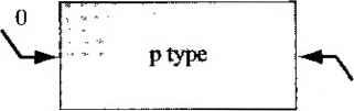 S DO x = 0 = W = 30X 10 cm s = 0 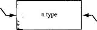 s(W) л = W = 20 x lOrcm Figure 6.22 I Figure for Problem 6.39. Figure 6.23 I Figure for Problem 6.40, Illumination s = 0 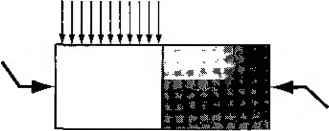 x=-W л = 0 Figure 6,24 I Figure for Problem 6.41. (a) Determine the steady-state excess minority carrier concentration versus x if the surface recombination velocity at jc = 0 is (/) s 0, {ii)s = 2000 cm/s, and (iii) s = oo. Ф) Calculate the excess minority carrier concentration at jc = 0 for {i)s= 0, (ii) s = 2000 cm/s, and (iii) s = oo, *6.39 (a) Consider the p-type semiconductor shown in Figure 6.22 with the following parameters: =5 x 10 cm~-, = 25 cm-/s, and r o = 5 x 10 s. The surface recombination velocities at the two surfaces are shown. The electric field is zero. The semiconductor is illuminated at jc = 0 with an excess-carrier generafion rate equal to = 2 x 10- cm~--s~. Determine the excess minority carrier electron concentration versus x in steady state, (b) Repeat part (o) for т^о oo. *6.40 Consider the n-type semiconductor shown in Figure 6.23. Assume that Dp = 10 cm /s and Tpo 00. The electric field is zero. Assume that a flux of excess electrons and holes is incident at x = 0. Let the flux of each carrier type be 10 carriers/cm--s. Determine the minority carrier hole current versus jc if the surface recombination velocity is (a) s(W) oo and (b) s(W) = 2000 cm/s. *6.41 A p-type semiconductor is shown in Figure 6.24. The surface recombination velocities are shown. The semiconductor is uniformly illuminated for - W < jc < 0 producing a constant excess-carrier generation rate Gq. Determine the steady-state excess-carrier concentration versus jc if the minority carrier lifetime is infinite and if the electric field is zero. 6.42 Plot 8p(x) versus x for various values of s using Equation (6.113). Choose reasonable parameter values. Summary and Review *6.43 Consider an n-type semiconductor as shown in Figure 6,21. The material is doped at Nj = 3 x 10 cm~ and Na = 0. Assume that Dp = 12cm-/s and Xpo = 2x 10 s. The electric field is zero. Design the surface recombination velocity so that the minority carrier diffusion current density at the surface is no grealer than Jp = -0.18 A/cm with a uniform excess-carrier generation rate equal to = 3 x 10 cm--s-. Reading List 6.44 Consider a semiconductor with excess carriers present. From the definition of carrier lifetimes and recombination rates, determine the average time that an electron stays in the conduction band and the average time that a hole stays in the valence band. Discuss these relations for (a) an intrinsic semiconductor and {h) an n-type semiconductor. 6.45 Design a gallium arsenide photoconductor that is 5 дт thick. Assume that т„() = Tpo 10- s and = 5x lOVm \ With an excitation of g = 10 cm--s , a photocurrent of at least 1 д A is desired with an applied voltage of 1 V. READING LIST 1. Bube, R. H. Photoelectronic Properties of Semiconductors, New York: Cambridge University Press, 1992. *2. deCogan, D. Solid State Devices: A Quantum Physics Approach. New York: Springer-Veriag, 1987. 3. Hall, R. H. Electron-Hole Recombination. Physical Review 87, no. 2 (July 15, 1952), p. 387. 4. Haynes, J. R., and W. Shockley. The Mobility and Life of Injected Holes and Electrons in Germanium. Physical Review 81, no. 5 (March 1, 1951), pp. 835-843. ♦5. Hess, K. Advanced Theory of Semiconductor Devices. Englewood Cliffs, NJ: Prentice Hall, 1988. 6. Kano, K. Semiconductor Devices, Upper Saddle River, NJ: Prentice Hall, 1998. 7. Kingston, R. H. Semiconductor Surface Physics. Philadelphia: University of Pennsylvania Press, 1957. 8. McKelvey, J. P Solid State Physics for Engineering and Materials Science. Malabar, FL.: Krieger Publishing, 1993. 9. Pierret, R. F. Semiconductor Device Fundamentals. Reading, MA: Addison-Wesley, 1996, m Shockley, W., and W T. Read, Jr. Statistics of the Recombinations of Holes and Electrons. Physical Review 87, no. 5 (September 1, 1952), pp. 835-842. 11. Singh, J. Semiconductor Devices: An Introduction. New York: McGraw-Hill, 1994. 12. Singh, J. Semiconductor Devices: Basic Principles, New York: John Wiley and Sons, 2(Ю1. 13. Streetman, B. G., and S. Banerjee. Solid State Electronic Devices. 5th ed. Upper Saddle River, NJ: Prentice Hall, 2000. *14. Wang, S. Fundamentals of Semiconductor Theory and Device Physics. Englewood Cliffs, NJ; Prentice HaU, 1989. СНА РЖ Е R  The pn Junction PREVIEW W to this point in the text, we have been considering the properties of the I semiconductor material. We calculated electron and hole concentrations in thermal equilibrium and determined the position of the Fermi level. We then considered the nonequilibrium condition in which excess electrons and holes are present in tiie semiconductor. We now wish to consider the situation in which a p-type and an n-type semiconductor are brought into contact with one another to form a pn junction. Most semiconductor devices contain at least one junction between p-type and n-type semiconductor regions. Semiconductor device characteristics and operation are intimately connected to these pn junctions, so considerable attention is devoted initially to this basic device. The pn junction diode itself provides characteristics that are used in rectifiers and switching circuits. In addition, the analysis of the pn junction device establishes some basic temiinology and concepts that are used in the discussion of other semiconductor devices. The fundamental analysis techniques used for the pn junction will also be applied to other devices. Understanding the physics of the pn junction is, therefore, an important step in the study of semiconductor devices. The electrostatics of the pn junction is considered in this chapter and the current-voltage characteristics of the pn junction diode are developed in the next chapter. 7.11 BASIC STRUCTURE OF THE pn JUNCTION Figure 7. la schematically shows the pn junction. It is important to realize that the entire semiconductor is a single-crystal material in which one region is doped with acceptor impurity atoms to form the p region and the adjacent region is doped with donor atoms to form the n region. The interface separating the n and p regions is referred to as the metallurgical junction. 7.1 Basic Structure of the pn Junction  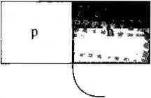 Metallurgical junction  Hole diffusion Electron diffusion X- 0 (b) Figure 7.1 I (a) Simplified geometry of a pn junction; (b) doping profile of an ideal uniformly doped pn junction. negative charge positive charge 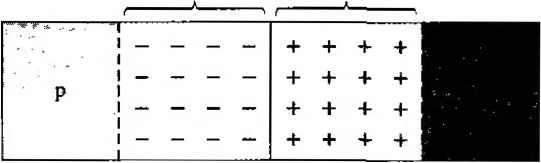 *Diffusion force on- holes Space charge region - E-field E-tleld E licki force on force on holes electrons Diffusion force on electrons Figure 7.2 I The space charge region, the electric field, and the forces acting on the charged carriers. The impurity doping concentrarions in the p and n regions are shown in Figure 7.1b. For simplicity, we will consider a step junction in which the doping concentration is uniform in each region and there is an abrupt change in doping at the junction. Inirially, at the metallurgical junction, there is a very large density gradient in both the electron and hole concentrations. Majority carrier electrons in the n region will begin diffusing into the p region and majority carrier holes in the p region will begin diffusing into the n region. If we assume there are no external connecrions to the semiconductor, then this diffusion process cannot conrinue indefinitely. As electrons diffuse from the n region, positively charged donor atoms are left behind. Similariy, as holes diffuse from the p region, they uncover negatively charged acceptor atoms. The net positive and negative charges in the n and p regions induce an electric field in the region near the metallurgical junction, in the direction from the positive to the negative charge, or from the n to the p region. The net positively and negatively charged regions are shown in Figure 7.2. These two regions are referred to as the space charge region. Essentially all electrons and holes are swept out of the space charge region by the electric field. Since the space charge region is depleted of any mobile charge, this region is also referred to as the depletion region; these two terms will be used interchangeably. Density gradients still exist in the majority carrier concentrations at each edge of the space charge region. We can think of a density gradient as producing a diffusion force that acts on the majority carriers. These diffusion forces, acting on the electrons and holes at the edges of the space charge region, are shown in the figure. The electric field in the ace charge region produces another force on the electrons and holes which is in the 1 ... 21 22 23 24 25 26 27 ... 55 |
|
© 2026 AutoElektrix.ru
Частичное копирование материалов разрешено при условии активной ссылки |