 |
 |
 |
| Главная Журналы Популярное Audi - почему их так назвали? Как появилась марка Bmw? Откуда появился Lexus? Достижения и устремления Mercedes-Benz Первые модели Chevrolet Электромобиль Nissan Leaf |
Главная » Журналы » Absorbing materialorganic polymer 1 ... 22 23 24 25 26 27 28 ... 55 opposite direction to the diffusion force for each type of particle. In thermal equilibrium, the diffusion force and the E-field force exactly balance each other. 7.2 I ZERO APPLIED BIAS We have considered the basic pn junction structure and discussed briefly how the space charge region is formed. In this section we will examine the properties of the step junction in thermal equilibrium, where no currents exist and no external excitation is applied. We will determine the space charge region width, electric field, and potential through the depletion region. 7,2Л Built-in Potential Barrier If we assume that no voltage is applied across the pn junction, then the junction is in thermal equilibrium-the Fermi energy level is constant throughout the entire system. Figure 7.3 shows the energy-band diagram for the pn junction in thermal equilibrium. The conduction and valance band energies must bend as we go through the space charge region, since the relative position of the conduction and valence bands with respect to the Fermi energy changes between p and n regions. Electrons in the conduction band of the n region see a potential barrier in trying to move into the conduction band of the p region. This potential barrier is referred to as the built-in potential barrier and is denoted by V/ -. The built-in potential barrier maintains equilibrium between majority carrier electrons in the n region and minority carrier electrons in the p region, and also between majority carrier holes in the p region and minority carrier holes in the n region. This potential difference across the junction cannot be measured with a voltmeter because new potential barriers will be formed between the probes and the semiconductor that will cancel V, The potential V[,i maintains equilibrium, so no current is produced by this voltage. The intrinsic Fermi level is equidistant from the conduction band edge through the junction, thus the built-in potential barrier can be determined as the difference Фрр Figure 7.3 I Energy-band diagram of a pn junction in thermal equilibrium. between the intrinsic Fermi levels in the p and n regions. We can define the potentials (/r and ф^р as shown in Figure 7.3, so we have Ф Ф (7.1) In the n region, the electron concentration in the conduction band is given by -{E, - Ef) Щ) - Nc exp which can also be written in the form (7.2) fiQ - Hi exp Ef - Efi kT (7.3) where n, and Ef, are the intrinsic carrier concentration and the intrinsic Fermi en-. ergy, respectively. We may define the potential фfn in the n region as Efi - Ef (7.4) Equation (7.3) may then be written as По - exp -(ефг„) кТ (7-5) Taking the natural log of both sides of Equation (7.5), setting no - Nj, and solving for the potential, we obtain Феп = - In - e V Similarly, in the p region, the hole concentration is given by Efi - Ef (7-6) A) - Na = rii exp (7-7) where is the acceptor concentration. We can define the potential фfp in the p region as e4fp = Efi - Ef (7.8) Combining Equations (7.7) and (7.8), we find that фрр^-\--In - e \ rii (7.9) Finally, the built-in potential barrier for the step junction is found by substituting Equations (7.6) and (7.9) into Equation (7.1), which yields 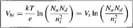 (7.10) where Ц ~ кТ/е and is defined as the thermal voltage. At this time, we should note a subtle but important point concerning notation. Previously in the discussion of a semiconductor material, Л/j and Л/ denoted donor and acceptor impurity concentrations in the same region* thereby forming a compensated semiconductor. From this point on in the text, Л^ and Na will denote the net donor and acceptor concentrations in the individual n and p regions, respectively. If the p region, for example, is a compensated material, then Na will represent the difference between the actual acceptor and donor impurity concentrations. The parameter Nii is defined in a similar manner for the n region. EXAMPLE 7.1 I Objective 8 -3 To calculate the built-in potential barrier in a pn junction. Consider a silicon pn junction at Г = 300 К wiih doping densities N = I x lO cm andAj = 1 X 10 cm \ Assume that= 1.5 x 10 cm~-\ Solution The built-in potential barrier is determined from Equation (7.10) as Vbi (0.0259) In 15\ П (I0**)(10) - 0Л54 V If we change the acceptor doping from N 1 x 10* cm lo = 1 x 10 cm \ but keep all other parameter values constant, then the built-in potential barrier becomes Vi = 0.635 V. Ш Comment The built-in potential barrier changes only slightly as the doping concentrations change by orders of magnitude because of the logarithmic dependence. TEST YOUR UNDERSTANDING E7.1 Calculate the built-in potential barrier in a silicon pn junction at 7 = 300 К for E7,2 {a) Л^, = 5 X 10 cm~\ Nj = 10 cm- and {h) N, 10 cm = 2 X 10* cm- [A SSO (0 Л 96Г0 ( ) Vl Repeat Е7Л for a GaAs pn junction. [A IT i4) Ч 9Z \ i) -uvl 7.2,2 Electric Field An electric field is created in the depletion region by the separation of positive and negative space charge densities. Figure 7.4 shows the volume charge density distribution in the pn junction assuming uniform doping and assuming an abrupt junction approximation. We will assume that the space charge region abruptly ends in the n region at X --л„ and abruptly ends in the p region at x quantity). -Xp (x, is a positive p (C/cmO P  Figure 7.41 The space charge density in a uniformly doped pn junction assuming the abrupt junction approximation. The electric field is determined from Poissons equation which, for a one-dimensional analysis, is й^-ф(х) -p{x) dEix) (7Л1) where ф{х) is the electric potential, E(x) is the electric field, p{x) is the volume charge density, and f 5 is the permittivity of the semiconductor. From Figure 7.4, the charge densities are p{x) - -eNa -Xp < JC < 0 p(x) - eN 0 < X < Xft (7.12a) (7.12b) The electric field in the p region is found by integrating Equation (7.11). We have that EfJdx-f-dx (7.13) where Ci is a constant of integration. The electric field is assumed to be zero in the neutral p region for x < -Xp since the currents are zero in thermal equilibrium. As there are no surface charge densities within the pn junction structure, the electric field is a continuous function. The constant of integration is determined by setting E = 0 at JC - -Xp. The electric field in the p region is then given by E --(x Л-Хр) -A> < JC < 0 (7.14) In the n region, the electric field is determined from -- dx =-X + C2 (7.15) where C2 is again a constant of integration. The constant C2 is determined by setting; E = 0 at X = , since the E-field is assumed to be zero in the n region and is a continuous function. Then (Xn - x) 0 < JC < (7 л 6) The electric field is also continuous at the metallurgical junction, or at x = 0. Setting Equations (7.14) and (7Л6) equal to each other at x = 0 gives NiiXp - NfjXjj (7Л7) Equation (7.17) states that the number of negative charges per unit area in the p region is equal to the number of positive charges per unit area in the n region. Figure 7.5 is a plot of the electric field in the depletion region. The electric field direction is from the n to the p region, or in the negative x direction for this geometry. For the uniformly doped pn junction, the E-field is a linear function of distance through the junction, and the maximum (magnitude) electric field occurs at the metallurgical junction. An electric field exists in the depletion region even when no voltage is applied between the p and n regions. The potential in the junction is found by integrating the electric field. In the p region then, we have E(x) dx (x -h Xp) dx (7.18) (7.19) where Cj is again a constant of integration. The potential difference through the pn junction is the important parameter, rather than the absolute potential, so we may arbitrarily set the potential equal to zero at x = -Xp. The constant of integration is 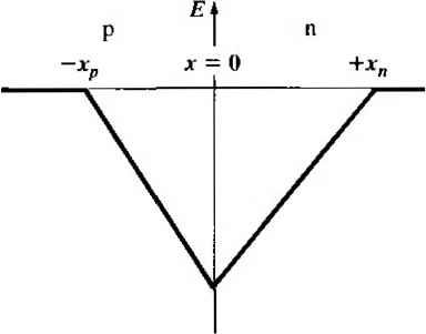 Figure 7.5 I Electric field in the space charge region of a uniformly doped pn junction. then found as so that the potential in the p region can now be written as (7.20) {X+Xpf i-Xn <x <0) (7.21) The potential in the n region is determined by integrating the electric field in the n region, or {x -x)dx (7.22) Then (7.23) where Cj is another constant of integration. The potential is a continuous function, so setting Equation (7.21) equal to Equation (7.23) at the metallurgical junction, or at x = 0, gives 1 = 4 (7.24) The potential in the n region can thus be written as ФМ = - * у j + (0 < < x ) (7.25) Figure 7.6 is a plot of the potential through the junction and shows the quadratic dependence on distance. The magnitude of the potential at x = x is equal to the
Figure 7.6 I Electric potential through the space charge region of a uniformly doped pn junction. built-m potential barrier. Then from Equation (7.25), we have ф(л x ) = - {Nxl + NaxD (7.26) The potential energy of an electron is given by £ = -еф, which means that the electron potential energy also varies as a quadratic function of distance through the space charge region. The quadratic dependence on distance was shown in the energy-band diagram of Figure 7.3, although we did not explicitly know the shape of the curve at that time. У 7.2.3 Space Charge Width We can determine the distance that the space charge region extends into the p and n regions from the metallurgical junction. This distance is known as the space charge width. From Equation (7Л 7), we may write, for example. (7.27) Then, substituting Equation (7.27) into Equation (7.26) and solving for л: , we obtain iNa + Ndj (7.28) Equation (7.28) gives the space charge width, or the width of the depletion region, Xn extending into the n-type region for the case of zero applied voltage. Similarly, if we solve forj£: from Equation (7.17) and substitute into Equation (7.26), we find
(7.29) where х^ is the width of the depletion region extending into the p region for the case of zero applied voltage. The total depletion or space charge width Wis the sum of the two components, or W = x + Xp Using Equations (7.28) and (7.29), we obtain (7.30) (7.31) The built-in potential barrier can be determined from Equation (7.10), and then the total space charge region width is obtained using Equation (7.31). Objective To calculate the space charge width and electric field in a pn junction. Consider a silicon pn junction at T = 300 К with doping concentrations of A = 10* cm- and N,t = 10 cm- Solution In Example 7T, we determined the built-in potential barrier as V/ = 0.635 V. From Equation (7.31), the space charge width is 111/2 2f л Уы 2(11.7)(8.85 X 10- *)(0.635) ~ 1.6 X 10- 0.951 X 10 cm = 0.951 дт 10 + 10- (10б)(Ш1-) Using Equations (7,28) and (7.29), we can find .r = 0.864 дт, and Xp = 0.086 дт. The peak electric field at the metallurgical junction, using Equation (7.16) for example, is -eNx, -(1.6 X 10-)(10)(0.864 x 10) 7s (ll.7)(8.85 X 10-) -1.34 X 10 V/ctn Comment The peak electric field in the space charge region of a pn junction is quite large. We must keep in mind, however, that there is no mobile charge in this region; hence there will be no drift current. We may also note, from this example, that the width of each space charge region is a reciprocal function of the doping concentration: The depletion region will extend further into the lower-doped region. EXAMPLE 7.2 TEST YOUR UNDERSTANDING e7.3 A silicon pn junction at Г = 300 К with zero applied bias has doping concentrations of = 5 X lO cm~ and = 5 x 10 cm~\ Determine x ,Xp, W, and E ШЭ 01 X 1П7 = л- SUV) E7.4 Repeat E7.3 for a GaAs pn junction, (шэ/д oi x 98 £ = Г' al ШЭ , oi X 9F9 Ж oi x 09*5 = шэ y oi x 09 = uy) 7.3 I REVERSE APPLIED BIAS If we apply a potential between the p and n regions, we will no longer be in an equilibrium condition-the Fermi energy level will no longer be constant through the system. Figure 7.7 shows the energy-band diagram of the pn junction for the case   Figure 7.7 J Energy-band diagram of a pn junction under reverse bias. when a positive voltage is applied to the n region with respect to the p region. As the positive potential is downward, the Fermi level on the n side is below the Fermi level on the p side. The difference between the two is equal to the applied voltage in units of energy. The total potential barrier, indicated by Ушл- has increased. The applied potential is the reverse-bias condition. The total potential barrier is now given by VtotaJ ~ \Фгп \ + \Фгр\ -h yR (7.32) where V/? is the magnitude of the applied reverse-bias voltage. Equation (7.32) can be rewritten as = Уы + Уп (7.33) i where V/ is the same built-in potential barrier we had defined in thermal equilibrium. 7.3.1 Space Charge Width and Electric Field Figure 7.8 shows a pn junction with an applied reverse-bias voltage V/?. Also indicated in the figure are the electric field in the space charge region and the electric field Eapp, induced by the applied voltage. The electric fields in the neutral p and n regions are essentially zero, or at least very small, which means that the magnitude of the electric field in the space charge region must increase above the thermabequilibrium value due to the applied voltage. The electric field originates on positive charge and terminates on negative charge; this means that the number of positive and negative charges must increase if the electric field increases. For given impurity doping concentrations, the number of positive and negative charges in the depletion region can be increased only if the space charge width W increases. The space charge width W increases, -app Figure 7.8 i A pn junction, with an applied reverse-bias voltage, showing the directions of the electric field induced by and the space charge electric field. therefore, with an increasing reverse-bias voltage Vr. We are assuming that the elec-uic field in the bulk n and p regions is zero. This assumption will become clearer in the next chapter when we discuss the current-voltage characteristics. In all of the previous equations, the built-in potential barrier can be replaced by the total potential barrier. The total space charge width can be written from Equation (7.31) as (7.34) showing that the total space charge width increases as we apply a reverse-bias vt>Jt-age. By substituting the total potential barrier У^ы into Equations (7.28) and (7.29), the space charge widths in the n and p regions, respectively, can be found as a func-Hon of applied reverse-bias voltage. Objective To calculate the width of the space charge region in a pn junction when a reverse-bias voltage is applied. Again consider a silicon pn junction at 7 = 300 К with doping concemrafions of = 10 cm- and = 10 cm \ Assume that = 1.5 x lO* cm and let Vr = 5Y Ш Solution The built-in potential barrier was calculated in Example 7.1 for this case and is Уы =0.635 V. The space charge width is determined from Equation (7.34). We have 2(11Л)(8.85х 10-)(0.635 + 5) 1.6 x 10- 10 -h 10 15 П (10)(10) so that EXAMPLE 7.3 W = 2.83 x 10- cm = 2.83 }im 1 ... 22 23 24 25 26 27 28 ... 55 |
|
© 2026 AutoElektrix.ru
Частичное копирование материалов разрешено при условии активной ссылки |