 |
 |
 |
| Главная Журналы Популярное Audi - почему их так назвали? Как появилась марка Bmw? Откуда появился Lexus? Достижения и устремления Mercedes-Benz Первые модели Chevrolet Электромобиль Nissan Leaf |
Главная » Журналы » Absorbing materialorganic polymer 1 ... 23 24 25 26 27 28 29 ... 55 Comment The space charge width has increased from 0.951 /im at zero bias to 2.83 дт at a reverse bias of5V. The magnitude of the electric field in the depletion region increases with an applied reverse-bias voltage. The electric field is still given by Equations (7.14) and (7.16) and is still a linear function of distance through the space charge region. Since Xn and Xp increase with reverse-bias voltage, the magnitude of the electric field also increases. The maximum electric field still occurs at the metallurgical junction. The maximum electric field at the metallurgical junction, from Equations (7.14Ш and (7.16), is n Ещах - -eNXfj -eNaX, (7,35] If we use either Equation (7.28) or (7.29) in conjunction with the total potential bar-* rier, Vbi + , then
(7.36) We can show that the maximum electric field in the pn junction can also be written as Ernax - -2{Уы + Ун) where W is the total space charge width. DESIGN EXAMPLE 7.4  Objecrive To design a pn junction to meet maximum electric field and voltage specifications. Consider a silicon pn junction at Г = 300 К with a p-type doping concentration of Na = 10** cm . Determine the n-type doping concentration such that the maximum electric field is [Emaxl = 3 X 10 V/cm at a reverse-bias voltage of Vf = 25 V. Solution The maximum electric field is given by Equation (7.36). Neglecting Уы compared to V, we can write lEfiiji I {lev. \Na+Nj 3 X 10 2(1.6 X 10)(25) / 10 (11.7)(8.85 X 10 ) which yields 1Л8 X 10 cm Conclusion A smaller value of results in a smaller value of lEixl for a given reverse-bias voltage. The value of determined in this example, then, is the maximum value that will meet the specifications. TEST YOUR UNDERSTANDING E7.5 (a) A silicon pn junction al T = 300 К is reverse-biased at -SV. The doping concentrations arc N =5 x 10 cm~ and Л^ -5 x 10 cm~-. Determine Xn.Xp, and lEpiaxI- (b) Repeat part (a) for a reverse bias voltage of Vr = 12 V. [ш^/А i-OI X teT = l 3l ги t-OI X 06T = M шэ o\ x = x uioOl X en = (Я) -шэ/л^О! X ПТ = Г Н1 шэ 01 х ig\ м *шэ 5 01 X ei7T = шэ от X et?T = ( ) suy] Е7.6 The maximum electric field in a reverse-biased GaAs pn junction at T = 300 К is to be lEiaxI =2.5 X 10 V/cm. The doping concentrations are Л^ = 5 x 10 cm~ and Л^ = 8 X 10* cm-. Determine the reverse-bias voltage that will produce this maximum electric field. (A £ZL пу) 7.3.2 Junction Capacitance Since we have a separation of ptsitive and negative charges in the depletion region, a capacitance is associated with the pn junction. Figure 7.9 shows the charge densities in the depletion region for applied reverse-bias voltages of Vr and Vr +dVR. An increase in the reverse-bias voltage dV will uncover additional positive charges in the n region and additional negative charges in the p region. The junction capacitance is defined as where Ш с (7.38) (7.39) dQ = eNj dxn - eN dXp The differential charge dQ is in units of C/cm so that the capacitance С is in units of farads per square centimeter (F/cm), or capacitance per unit area. For the total potential barrier. Equation (7.28) may be written as HI 1/2 2ev(Vft, + Vr) (7.40) The junction capacitance can be written as , G dx., С = = eN so that  With applied V. Wilh applied + dVf dx - Figure 7.9 I Differential change in the space charge width with a differential change in reverse-bias voltage for a uniformly doped pn junction. (7.43 Exactly the same capacitance expression is obtained by considering the space charge region extending into the p region Xp. The junction capacitance is also referred to а the depletion layer capacitance. EXAMPLE 7,5 Objective To calculate the junction capacitance of a pn junction. Consider the same pn junction as that in Example 7.3. Again assume that Vp -5\. Solution The junction capacitance is found from Equation (7.42) as С (1.6 X IQ )(11.7)(8.85 X 10-)(10Ъ(10) 2(0.635+ 5)(10 + 105) С =3.66 X 10 F/cm 7 щ 3 Reverse Applied Bias If the cross-sectional area of the pn junction is, for example, A = 10 cm-, then the total junction capacitance is CCA= 0.366 x 10-F = 0.366 pF Comment The value of junction capacitance is usually in the pF, or smaller, range. If we compare Equation (7.34) for the total depletion width IV of the space charge region under reverse bias and Equation (7.42) for the junction capacitance C\ we find that we can write (7.43) Equation (7.43) is the same as the capacitance per unit area of a parallel plate capacitor. Considering Figure 7.9, we may have come to this same conclusion earlier. Keep in mind that the space charge width is a function of the reverse bias voltage so that the junction capacitance is also a function of the reverse bias voltage applied to the pn junction. 73.3 One-Sided Junctions Consider a special pn junction called the one-sided junction. If, for example, this juncrion is referred to as a pn junction. The total space charge width, from Equation (7.34), reduces to Уы + Vr) ] (7.44) Considering the expressions forx and Xp, we have for the pn junction Xn < Xf, (7.45) (7.46) Almost the entire space charge layer extends into the low-doped region of the junction. This effect can be seen in Figure 7.10. The juncrion capacitance of the pn junction reduces to 2(Vbi + Vr) (7.47) The depletion layer capacitance of a one-sided junction is a function of the doping concentration in the low-doped region. Equarion (7.47) may be manipulated to give 204M:jv (7.48) --V,  Figure 7.10 I Space charge density of a one-sided p+n junction. 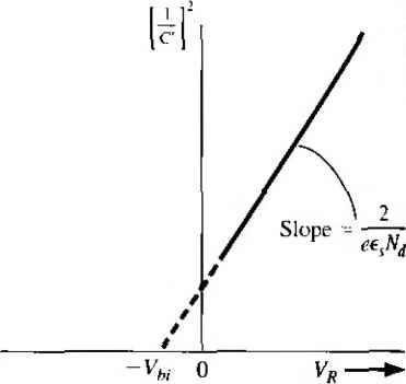 Figure 7.11 I {\/Cf versus Vr of a uniformly doped pn junction. which shows that the inverse capacitance squared is a hnear function of applied reverse-bias voltage. Figure 7.11 shows a plot of Equation (7.48). The built-in potential of the junction can be determined by extrapolating the curve to the point where (1 / CY - 0. The slope of the curve is inversely proportional to the doping concentration of the low-doped region in the junction; thus, this doping concentration can be experimentally determined. The assumptions used in the derivation of this capacitance include uniform doping in both semiconductor regions, the abrupt junction approximation, and a planar junction. EXAMPLE 7.6 Objective To determine the impurity doping concentrations in a p+n junction given the parameters from Figure 7.11. Assume a silicon p+n junction at Г = 300 К with = 1.5 x 10* cm *. Assume that the intercept of the curve in Figure 7.11 gives V = 0.855 V and that the slope is 1,32 X 10(F/cm)- (V)-i. Solution The slope of the curve in Figure 7.U is given by l/eeN, so we may write £e,(slope) (1.6 X 10⁻¹)(П.7)(8.85 x 10-)(1.32 x lOj 15 -3 =9.15 X 10 cm 7.4 Nonuniiorm}y Doped Junctions m the expression for V which h № can solve for as ? /еУы\ {1.5xl0<)= / 0.855 \ - = ]4tfj= 9.15 X 10- Hj rich yields iV = 534 x 10 cm-- Comment The results of this example show that N, therefore the assumption of a one-sided juitction was valid. A one-sided pn junction is useful for experimentally determining the doping concentrations and built-in potential. TEST YOUR UNDERSTANDING E7J A silicon pn junction at Г 300 К has doping concentrations of jV 3 x 10 cm and At, = 8 x 10 cm, and has a cross-sectional area of Л =5 x ]0~ cm. Determine the junction capacitance at (a) = 2 V and (t) VV 5 V. iJd LYO iq) 17690 i) -suvl E7.8 The experimentally measured junction capacitance of a one-sided silicon n p junction biased at V? 4 V at Г = 300 К is С = 1.10 pF. The built-in potential barrier is found to be V;, = 0,782 V. The cross-sectional area is Л 10 * cm, Find the doping concentrations. (- ifil UV=N gfil L N sV) =7.4 I NONUNIFORMLY DOPED JUNCTIONS In the pn junctions considered so far, we have assumed that each semiconductor region has been uniformly doped. In actual pn junction structures, this is not always true. In some electronic applications, specific nonuniform doping profiles are used to obtain special pn junction capacitance characteristics. 7A1 Linearly Graded Junctions If we start with a uniformly doped n-type semiconductor, for example, and diffuse acceptor atoms through the surface, the impurity concentrations will tend to be like those shown in Figure 7.12. The point x - jc on the figure corresponds to the metallurgical junction. The depletion region extends into the p and n regions from the metallurgical junction as we have discussed previously. The net p-type doping 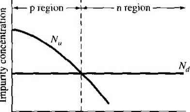 Surface Figure 7.12 f Impurity concentrations of a pn junction with a nonuniformly doped p region. p region 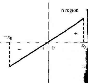 Figure 7.13 I Space charge density linearly graded pn junction. concentration near the metallurgical junction may be approximated as a linear fui tion of distance from the metallurgical junction. Likewise, as a first approximat the net n-type doping concentration is also a linear function of distance extenc into the n region from the metallurgical junction. This effective doping profile referred to as a linearly graded junction. Figure 7.13 shows the space charge density in the depletion region of the early graded junction. For convenience, the metallurgical junction is placed atx = The space charge density can be written as where й is the gradient of the net impurity concentration. The electric field and potential in the space charge region can be determh from Poissons equation. We can write so that the electric field can be found by integration as eax / 2 24 - dx~{x -X,) The electric field in the linearly graded junction is a quadratic function of dist rather than the linear function found in the uniformly doped junction. The maximi electric field again occurs at the metallurgical junction. We may note that the electri< field is zero at both x = -f jcq and at л - - Xo. The electric field in a nonuniform! doped semiconductor is not exactly zero, but the magnitude of this field is small, so setting E = 0 in the bulk regions is still a good approximation. The potential is again found by integrating the electric field as (7.52)  7.4 Nonuniformly DopedJunctions 2S7 If we arbitrarily set 0 at x = -xq, then the potential through the junction is -ea (x л \ ea The magnitude of the potential at jc - -f-.vo will equal the built-in potential barrier for this function. We then have that 2 eaxi Ф(хо) - T -Уы (7-54) Another expression for the built-in potential barrier for a linearly graded junction can be approximated from the expression used for a uniformly doped junction. We can write  Уы - Уг In (7.55) where Ndixo) and Na{-Xo) are the doping concentrations at the edges of the space charge region. We can relate these doping concentrations to the gradient, so that N,f(xo) axQ (7.56a) K(-JCq) - axQ (7.56b) Then the built-in potential barrier for the linearly graded junction becomes V,- = V,ln (7.57) There may be situations in which the doping gradient is not the same on either side of the junction, but we will not consider that condition here. If a reverse-bias voltage is applied to the junction, the potential barrier increases. The built-in potential barrier 14,- in the above equations is then replaced by the total potential barrier Vfyi + Уц. Solving for xo from Equation (7.54) and using the total potential barrier, we obtain  хо=-\1~(Уы + Ун) [2 ea (7.58) The junction capacitance per unit area can be determined by the same method as we used for the uniformly doped junction. Figure 7.14 shows the differential charge dQ which is uncovered as a differential voltage dV \s applied. The junction capacitance is then . dQ dxo С =:~ = (eaxo) (7.59) dVR dVR p (C/cm) t C P n) A> = 4) do 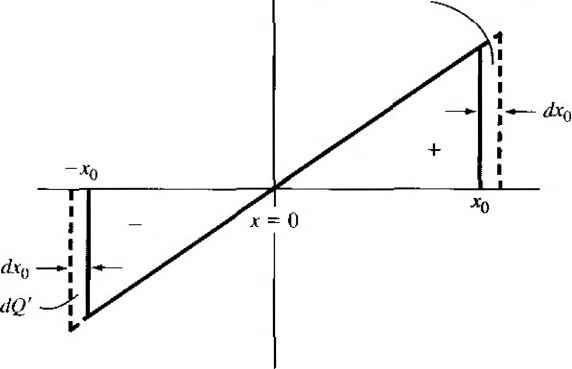 Figure 7Л4 I Differential change in space charge width with a differential change in reverse-bias voltage for a linearly graded pn junction. Using Equation (7.58), we obtain С eae: (7.60) We may note that С is proportional to (Уы + V)~ for the linearly graded junction as compared to С'а{Уы + V/)~ for the uniformly doped junction. In the linearly graded junction, the capacitance is less dependent on reverse-bias voltage than in the uniformly doped junction. 7.4.2 Hyperabrupt Junctions The uniformly doped junction and linearly graded junction are not the only possible doping profiles. Figure 7.15 shows a generalized one-sided p+n junction where the generalized n-type doping concentration for x > 0 is given by N = Bx (7.61) The case of m 0 corresponds to the uniformly doped junction and m = -fl corresponds to the linearly graded junction just discussed. The cases of m = -1-2 and m = +3 shown would approximate a fairly low-doped epitaxial n-type layer grown on a much more heavily doped n+ substrate layer. When the value ofm is negative, we have what is referred to as a hyperabrupt junction. In this case, the n-type doping is larger near the metallurgical junction than in the bulk semiconductor. Equation (7.61) is used to approximate the n-type doping over a small region near x - jcq and does not hold at X = 0 when m is negative. In a more exact analysis, Уы in Equation (7.60) is replaced by a gradient voltage. However, this analysis is beyond the scope of this text.
Figure 7.15 [ Generalized doping profiles of a one-sided p+n junction. (From Sze [141} The junction capacitance can be derived using the same analysis method as be-)ге and is given by \Пт+2) (7.62) ten m is negative, the capacitance becomes a very strong function of reverse-bias voltage, a desired characteristic in varactor diodes. The term varactor comes from the words variable reactor and means a device whose reactance can be varied in a controlled manner with bias voltage. If a varactor diode and an inductance are in parallel, the resonant frequency of the LC circuit is (7.63) The capacitance of the diode, from Equation (7.62), can be written in the form С = Co{Vw + Уд)-/ +2> (7.64) In a circuit application, we would, in general, like to have the resonant frequency be Ilinear function of reverse-bias voltage Vr, so we need С (x V (7.65) 1 ... 23 24 25 26 27 28 29 ... 55 |
|||||||||||||||||||||||||||
|
© 2026 AutoElektrix.ru
Частичное копирование материалов разрешено при условии активной ссылки |