 |
 |
 |
| Главная Журналы Популярное Audi - почему их так назвали? Как появилась марка Bmw? Откуда появился Lexus? Достижения и устремления Mercedes-Benz Первые модели Chevrolet Электромобиль Nissan Leaf |
Главная » Журналы » Absorbing materialorganic polymer 1 ... 24 25 26 27 28 29 30 ... 55 260 С Н А Р Т Е R 7 The pn Junction From Equation (7.64), the parameter m required is found from m + 2 = 2 (7.66a A specific doping profile will yield the desired capacitance characteristic. 7.5 I SUMMARY Ш A imitomily doped pn juncuon was initially considered, in which one region of a semiconductor is uniformly doped with acceptor impurities and the adjacent region is uniformly doped with donor impurities. This type of junction is called a homoj unction. A space charge region, or depletion region, is formed on either side of the metallurgical junction separating the n and p regions. This region is essentially depleted of any mobile electrons or holes. A net positive charge density, due to the positively charged donor impurity ions, exists in the n region and a net negative charge density, due to the negatively charged acceptor impurity ions, exists in the p region. An electric field exists in the depletion region due to the net space charge density. The direction of the electric field is from the n region to the p region. A potential difference exists across the space-charge region. Under zero applied bias, this potential difference, known as the built-in potential barrier, maintains thermal equilibrium and holds back majority carrier electrons in the n-region and majority carrier holes in the p region. An applied reverse bias voltage (n region positive with respect to the p region) increases the potential barrier iticreases the space charge width, and increases the magnitude of the electric field. As the reverse bias voltage changes, the amount of charge in the depletion region changes. This change in charge with voltage defines the junction capacitance. The linearly graded junction represents a nonuniformly doped pn junction. Expressions for the electric field, built-in potential barrier, and junction capacitance were derived. The functional relationships differ from those of the uniformly doped junction. Specific doping profiles can be used to obtain specific capacitance characteristics. A hyperabrupt junction is one in which the doping decreases away from the metallurgical junction. This type of junction is advantageous in varactor diodes that are used in resonant circuits. GLOSSARY OF IMPORTANT TERMS abrupt j unction approximation The assumpfion that there i s an abrupt discontin uity i n space charge density between the space charge region and neutral semiconductor region. built-in potential harrier The electrostatic potential difference between the p and n regions of a pn junction in thermal equilibrium. depletion layer capacitance Another term for junction capacitance. depletion region Another term for space charge region. hyperabrupt junction A pn junction in which the doping concentration on one side decreases away from the metallurgical junction to achieve a specific capacitance-voltage characteristic. Junction capacitance The capacitance of the pn junction under reverse bias. lineariy graded junction A pn junction in which the doping concentrarions on either side of the metallurgical junction are approximated by a linear distriburion. metailurgical junction The interface between the p- and n-doped regions of a pn junction. one-sided junction A pn junction in which one side of the juncrion is much more heavily doped than the adjacent side. reverse bias The condition in which a positive voltage is applied to the n region with respect to the p region of a pn junction so that the potential barrier between the two regions increases above the thermal-equilibrium built-in potential barrier space charge region The region on either side of the metallurgical junction in which there is a net charge density due to ionized donors in the n-region and ionized acceptors in the p region. space charge width The width of the space charge region, a function of doping concentrations and applied voltage. varactor diode A diode whose reactance can be varied in a controlled manner with bias voltage. CHECKPOINT After studying this chapter, the reader should have the ability to: Describe why and how the space charge region is formed. Draw the energy band diagram of a zero-biased and reverse-biased pn junction. Define and derive the expression of the built-in potential barrier voltage. Derive the expression for the electric field in space charge region of the pn junction. Describe what happens to the parameters of the space charge region when a reverse bias voltage is applied. Define and explain the junction capacitance. Describe the characteristics and properties of a one-sided pn junction, Describe how a linearly graded junction is formed. Define a hyperabrupt j unction. REVIEW QUESTIONS L Define the built-in potential voltage and describe how it maintains thermal equilibrium. 2. Why is an electric field formed in the space charge region? Why is the electric field a linear function of distance in a uniformly doped pn junction? 3. Where does the maximum electric field occur in the space charge region? 4. Why is the space charge width larger in the lower doped side of a pn junction? 5. What is the functional dependence of the space charge width on reverse bias voltage? 6. Why does the space charge width increase with reverse bias voltage? 7. Why does a capacitance exist in a reverse-biased pn junction? Why does the capacitance decrease with increasing reverse bias voltage? PROBLEMS Section 7.2 Zero Applied Bias 7.1 {a} Calculate in a silicon pn junction at Г = 300 К for (a) Nj = 10 cm and = (/) 10\ ( ) 10 (iii) \0\ (iv) 10 cm-\ (h) Repeat part (a) for N,i = 10 cm-\ 7.2 Calculate the built-in potential barrier, Ц>>, for Si, Ge, and GaAs pn junctions if they each have the following dopant concentrations at Г = 300 К: (a) Ki = 10 cm Na = 10 cm - [h] Nj = 5x 10 /V = 5 X lO* (c) Nj = 10 N, = 10 7.3 (a) Plot the built-in potential barrier for a symmetrical {N = N) silicon pn junction at r = 300 К over the range 10- < N, = Nj < 10 cm- (b) Repeat part (a) for a GaAs pn junction. 7.4 Consider a uniformly doped GaAs pn junction with doping concentrations of N = 5 X 10 cm * and =5 x 10 cm~ Plot the built-in potential barrier voltage, Vtyj, versus temperature for 200 <T < 500 K. 7.5 An abrupt sihcon pn junction at zero bias has dopant concentrations of Л', = 10cm -* and Nj = 5 x \0 cm~\ T = 300 K. (a) Calculate the Fermi level on each side of the junction with respect to the intrinsic Fermi level. (/?) Sketch the equilibrium energy-band diagram for the junction and determine V/ from the diagram and the results of part {а).(с) Calculate 14, using Equation (7.10), and compare the results to part (b). (d) Determine x , .r and the peak electric field for this junction. 7.6 Repeat problem 7.5 for the case when the doping concentrations are N = Nj = 2 x 10cm--\ 7.7 A silicon abrupt junction in thermal equilibrium at Г = 300 К is doped such that E - Ef = 0.21 eV in the n region and Ef. - £, = 0.18 eV in the p region. (a) Draw the energy band diagram of the pn junction, (h) Determine the impurity doping concentrations in each region, (c) Determine V/ . 7.8 Consider the uniformly doped GaAs junction at Г = 300 К. At zero bias, only 20 percent of the total space charge region is to be in the p region. The built-in potential barrier is Уы = 1.20 V. For zero bias, determine (a) Na, (h) jVj, (c) jc , id)Xp, and (e) -max* 7.9 Consider the impurity doping profile shown in Figure 7.16 in a silicon pn junction. For zero applied voltage, (a) determine Уы, (i) calculate л„ and Xp, (c) sketch the thermal equilibrium energy band diagram, and (d) plot the electric field versus distance through the junction. 8. What is a one-sided pn junction? What parameters can be determined in a one-sided pn junction? 9, What is a Hnearly graded junction? 10. What is a hyperabrupt junction and what is one advantage or characteristic of such a junction? Probiems ptype -4 X 10 2 fim n type Figure 7Л6 I Figure for Probleiu 7.9, Figure 7.17 I Figure for Problem 7.12. *7.10 A uniformly doped silicon pn junction is doped to levels of N,i =5 x lO cm and = lO* cm~\ The measured built-in potential barrier is Vf = 0.40 V. Deteriuine the temperature at which this result occurs. (You may have to use trial and error to solve this problem.) 7Л1 Consider a uniformly doped silicon pn junction with doping concentrations A = 5 x 10 cm- and = 10 cm-\ (a) Calculate at T = 300 K. {b) Determine the temperature at which Vii decreases by 1 percent. 7.12 An isotype step junction is one in which the same impurity type doping changes from one concentration value to another value. An n-n isotype doping profile is shown in Figure 7.17. (fO Sketch the thermal equilibrium energy band diagram of the isotype junction, (b) Using the energy band diagratn, deterinine the built-in potenfial barrier (c) Discuss the charge distribution through the junction. A particular type of junction is an n region adjacent to an intrinsic region. This junction can be modeled as an n-type region to a lightly doped p-type region. Assume the doping concentrations in silicon at T = 300 К are = 10 cin and jV = 10- cm *. For zero applied bias, determine (<r/) Vti, {b) jc , (c) Xp, and (J) E Sketch the electric field versus distance through the junction. 7.14 We are assuming an abrupt deplefion approximation for the space charge region. That is, no free carriers exist within the deplefion region and the semiconductor abruptly changes to a neutral region outside the space charge region. This approximation is adequate for most applications, but the abrupt transition does not exist. The space charge region changes over a distance of a few Debye lengths, where the Debye length in the n region is given by Calculate Lo and find the ratio of Lu/x,i for the following conditions. The p-type doping concentration is JV = 8 x 10 cm~ and the n-type doping concentration is -cm- 7.15 (a) jVj = 8 x 10 cm-\ (h) = 2.2 x 10 cm and (c) Л/j = 8 x 10 Examine how the electric field versus distance through a uniformly doped pn junction varies as the doping concentrations vary. For example, consider = 10 cm- and let lO < iV < 10 cm--\ then consider Л^ = 10 cm- and let  10 < Na S 10 cm--\ and iinally consider Nj = 10 cm - and let 10 <K< 10 cm-\ What can be said about the results for Na > WONj or Nj > lOONJ Assume zero applied bias. Section 7.3 Reverse Applied Bias 7Л6 An abrupt silicon pn junction has dopant concentrations of N - 2 x 10 cm and N=2x10 cm-- at T = 300 K. Calculate (a) Уы, Ф) W at V/ = О and l/>f = 8 V, and (c) the maximum electric field in the space charge region at V = 0 and Vr = 8 V 7.17 Consider the junction described in Problem 7.11, The junction has a cross-sectional area of lO cm and has an applied reverse-bias voltage of Уц =5 V. Calculate (a) Уы, Ф) Xft.Xp, (c) Emax, and (d) the total junction capacitance. 7.18 An ideal one-sided silicon np junction has uniform doping on both sides of the abrupt junction. The doping relation is Ni = SON. The built-in potential barrier is Уы = 0.752 V. The maximum electric field in the junction is E = 1.14 x lO V/cm for a reverse-bias voltage of 10 V. Г = 300 К. Determine {a) N, Nj Ф) Xp for Vfi = 10, and (c) C; for У^ 10. 7.19 A silicon n+p junction is biased at = 10 V. Determine the percent change in (a) junction capacitance and Ф) built-in potential if the doping in the p region increases by a factor of 2. 7.20 Consider two pn silicon junctions at T = 300 К reverse biased at V/? = 5 V. The impurity doping concentrations injunction A are N - 10 cm and N,i - cm -\ and those injunction В wrc N = 10* cm and Nj = 10 cm~ Calculate the ratio of the following parameters for junction A to junction B: (a) Ф) lEniaxI, and (c)C. 7.21 (a) The peak electric field in a reverse-biased silicon pn junction is lEmaxI = 3 X 10 V/cm. The doping concentrations are Nj = 4 x 10** cm~ and Na = 4 X 10 cm~ . Find the magnitude of the reverse-bias voltage, ф) Repeat part (a) for = 4 x 10 cm * and N - 4x 10 cm . (c) Repeat part {a) for Л^,; =N.=4x 10⁴m--\ 7.22 Consider a uniformly doped GaAs pn junction at Г = 300 К. The junction capacitance at zero bias is Cj{0) and the junction capacitance with a 10-V reverse-bias voltage is Cj (10), The ratio of the capacitances is =3.13 СД10) Also under reverse bias, the space charge width into the p region is 0.2 of the total space charge width. Determine {a) Уы and ф) N, Nd- 7-23 GaAs pn junction at Г = 300 К has impurity doping concentrations of N = 10 cm and N(j =5 X 10 cm~-. For a particular device application, the ratio of junction capacitances at two values of reverse bias voltage must be C (i) / Cj (V2) - 3 where the reverse bias voltage V>f i = 1 V. Determine V2. 7.24 An abrupt silicon pn junction at T = 300 К is uniformly doped with N = 10** cm * and Nj = lO* cm~*. The pn junction area is 6 x 10 cm. An inductance of 2.2 millihenry is placed in parallel with the pn junction. Calculate the resonant frequency of the circuit for reverse-bias voltages of (a) V/f = 1 V and Ф) Vr = 10 V   +5 X 10  -Ш Figure 7Л8 I Figure for Problem 7.27. Figure 7.19 I Figure for Problem 7.28. 7.25 7.26 7.27 7.28 7.29 7.30 7.31 A uniformly doped silicon p+n junction at 7 = 300 К is to be designed such that at a reverse-bias voltage of V;? = 10 V, the maximum electric field is limited to Emjix = 10* V/cm. Determine the maxiium doping concentrafion in the n region. A silicon pn junction is to be designed which meets the following specifications at T = 300 K. At a reverse-bias voltage of 1.2 V, 10 percent of the total space charge region is to be in the n region and the total junction capacitance is to be 3.5 x 10 F with a cross-sectional area of 5.5 x lO cnr. Detennine {a) JV , (/?) Л^,/, and (c) Уы. A silicon pn junction at Г = 300 К has the doping profile shown in Figure 7.18. Calculate (a) V/,;, (h) and Xp at zero bias, and (c) the applied bias required so that Xn = 30 дт. Consider a silicon pn junction with the doping profile shown in Figure 7.19. T = 300 K. (a) Calculate the applied reverse-bias voltage required so that the space charge region extends entirely through the p region, (h) Determine the space charge width into the n -region with the reverse-bias voltage calculated in part (a), (c) Calculate the peak electric field for this applied voltage. (fl) A silicon p n junction has doping concentrations of = 10 cm~ and jVj =5 X 10- cm -. The cross-sectional area of the junction is Л =5 x 10~ cm. Calculate the junction capacitance for {i)VR =0,(u)Vr = 3 V, and ( /) Vr = 6 V. Plot 1/C versus Vr . Show that the slope of the curve can be used to find Nd and that the intersection with the voltage axis yields Уы. (b) Repeat part (a) if the n-type doping concentration changes io = 6 x 10 cm~\ The total juncrion capacitance of a one-sided silicon pn junction at Г = 300 К is measured at V/? =50 mV and found to be 1.3 pF. The junction area is 10 cm and Vfyi - Q.95 \. (a) Find the impurity doping concentration of the low-doped side of the junction, (b) Find the impurity doping concentration of the higher-doped region. Examine how the capacitance С and the function {l/C) vary with reverse-bias voltage Vfi as the doping concentrations change. In particular, consider these plots versus N for N > and versus N,! for N,j > 100/V,. A pn junction has the doping profile shown in Figure 7.20. Assume that x > xq for all reverse-bias voltages, (a) What is the built-in potential across the junction? (b) For   о {Nj - NA {cm-- ) -2 -1 -5 X 10 5 x 10 + 1 +2 I u i region л ifim) Figure 7.20 I Figure for Problem 7.32. Figure 7.21 I Figure for Problem 7.33. the abrupt junction approximation, sketch the charge density through the junction. (c) Derive the expression for the electric field through the space charge region. *7.33 A silicon PIN junction has the doping profile shown in Figure 7.21. The corresponds to an ideal intrinsic region in which there is no impurity doping concentration. A reverse-bias voltage is applied to the PIN junction so that the total depletion width extends from -2 mto+2 jum. (й) Using Poissons equation, calculate the magnitude of the electric field at x = 0, (b) Sketch the electric field through the PIN junction, (c) Calculate the reverse-bias voltage that must be applied. Section 7.4 Nonuniformly Doped Junctions 7.34 7.35 Consider a hnearly graded junction, {a) Starting with Equation (7.49), derive the expression for the electric field given in Equation (7.51). {b) Derive the expression for the potential through the space charge region given by Equation (7.53). The built-in potential barrier of a linearly graded silicon pn junction at Г = 300 К is 14,- 0.70 V. The junction capacitance measured atV/? =3.5VisC = 7.2x 10 F/cm . Find the gradient, й, of the net impurity concentration.  Summary and Review 7.36 A one-sided p+n silicon diode at T = 300 К is doped al /V = 10 cm . Design the junction so that Cy = 0.95 pF at V/? = 3.5 V. Calculate the junction capacitance when V = 1.5V. 7.37 A one-sided p n junction with a cross-sectional area of 10 ** cm has a measured built-in potential of Уы = 0.8 V at Г = 300 К. A plot of (1/Cj) versus is linear for V/? < 1 V and is essentially constant for V/? > 1 V. The capacitance is Cy = 0.082 pF at V/? = 1 V, Determine the doping concentrations on either side of the metallurgical junction that will produce this capacitance characteristic. *7.38 Silicon, at Г = 300 К, is doped at Л^, = lO-** cm for x < 0 and Nj2 = 5 x 10 cm for .T > 0 to form an л - n step junction, (a) Sketch the energy-band diagram, (b) Derive an expression for V/,. (c) Sketch the charge density, electric field, and potential through the Junction, (d) Explain where the charge density came from and is located. *7.39 A diffused silicon pn junction has a linearly graded junction on the p side with fl = 2 x 10 cm , and a uniform doping of 10- cm on the n side, (a) If the Reading List 267 depletion width on the p side is OJ дт at zero bias, find the total depletion width, built-in potential, and maximum electric field at zero bias, {b) Plot the potential function through the junction. READING LIST 1. Dimitrijev, S. Understanding Semiconductor Devices, New York: Oxford University Press, 2000. 2. Kano, K. Semiconductor Devices. Upper Saddle River, NJ: Prentice Hall, 1998. *3. Li, S. S. Semiconductor Physical Electronics. New York: Plenum Press, 1993. 4. Muller, R. S., and T. I. Kamins. Device Electronics for Integrated Circuits. 2nd ed. New York: Wiley, 1986. 5. Navon, D. H. Semiconductor Microdevices and Materials. New York: Holt, Rinehart & Winston, 1986. 6. Neudeck, G. W. The PN Junction Diode. Vol. 2 of the Modular Series on Solid State Devices. 2nd ed. Reading, MA: Addison-Wesley, 1989. *7, Ng, K. K. Complete Guide to Semiconductor Device.. New York: McGraw-Hill, 1995. 8. Pierret, R. R Semiconductor Device Fundamentals. Reading, MA: Addison-Wesley, 1996. *9. Roulston, D. J. Л/7 Introduction to the Physics of Semiconductor Devices. New York: Oxford University Press, 1999. 10. Shur, M. Introduction to Electronic Devices. New York: John Wiley and Sons, 1996. *11. Shur, M. Physics of Semiconductor Devices. Englewood Cliffs, NJ: Prentice Hall, 1990. 12. Singh, J. Semiconductor Devices: Basic Principles. New York: John Wiley and Sons, 2001. 13. Streetman, B.C., and S. Banerjee. Solid State Electronic Device., 5 th ed. Upper Saddle River, NJ: Prentice-Hal I, 2000. 14. Sze, S. M. Physics of Semiconductor Devices. 2nd ed. New York; Wiley, 1981. 15. Sze, S. M. Semiconductor Devices: Physics and Technology, 2nd ed. New York: John Wiley and Sons, Inc., 2001. *16. Wang, S. Fundamentals of Semiconductor Theory and Device Physics. Englewood Cliffs, NJ: Prentice Hall, 1989. 17. Yang, E, S. Microelectronic Devices. New York: McGraw-Hill, 1988.  CHAPTER о The pn Junction Diode PREVIEW In the last chapter, we discussed the electrostatics of the pn junction in thermal equilibrium and under reverse bias. We determined the built-in potential barrier at thermal equilibrium and calculated the electric field in the space charge region. We also considered the junction capacitance. In this chapter, we will consider the pn junction with a forward-bias voltage applied and will determine the current-voltage characteristics. The potential barrier of the pn junction is lowered when a forward-bias voltage is applied, allowing electrons and holes to flow across the space charge region. When holes flow from the p region across the space charge region into the n region, they become excess minority carrier holes and are subject to the excess minority carrier diffusion, drift, and recombination processes discussed in Chapter 6. Likewise, when electrons from the n region flow across the space charge region into the p region, they become excess minority carrier electrons and are subject to these same processes. When semiconductor devices with pn junctions are used in linear amplifiers, for example, time-varying signals are superimposed on the dc currents and voltages. A small sinusoidal voltage superimposed on a dc voltage applied across a pn junction will generate a small-signal sinusoidal current. The ratio of the sinusoidal current to voltage yields the smalUsignal admittance of the pn junction. The admittance of a forward-biased pn junction contains both conductance and capacitance terms. The capacitance, called a diffusion capacitance, differs from the junction capacitance discussed in the last chapter. Using the admittance function, the small-signal equivalent circuit of the pn junction will be developed. The last three topics considered in this chapter are junction breakdown, switching transients, and the tunnel diode. When a sufficiently large reverse-bias voltage is applied across a pn junction, breakdown can occur, producing a large reverse-bias current in the junction, which can cause heating effects and catastrophic failure of the diode. Zener diodes, however, are designed to operate in the breakdown region. Breakdown puts limits on the amount of voltage that can be applied across a pn junction. When a pn junction is switched from one conducting state to the other, transients in the diode current and voltage occur. The switching time of the pn junction will be discussed here, and again in later chapters which deal with the switching of transistors. 8.1 I pn JUNCTION CURRENT When a forward-bias voltage is applied to a pn junction, a current will be induced in the device. We initially consider a qualitative discussion of how charges flow in the pn junction and then consider the mathematical derivation of the current-voltage relationship. 8.1Л Qualitative Description of Charge Flow in a pn Junction We can qualitatively understand the mechanism of the current in a pn junction by again considering the energy band diagrams. Figure 8.1a shows the energy band diagram of a pn junction in thermal equilibrium that was developed in the last chapter. We argued that the potential barrier seen by the electrons, for example, holds back the large concentration of electrons in the n region and keeps them from flowing into the p region. Similarly, the potential barrier seen by the holes holds back the large 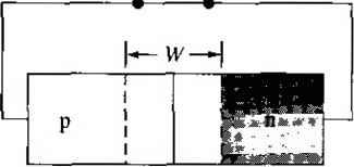 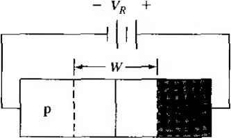 + v - ------ 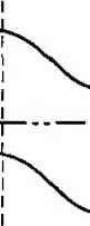 ----£f, Fp 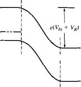 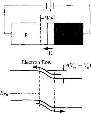 I..:----jr I----E Hole flow (fl) Figure 8.1 IA pn juncrion and its associated energy band diagram for (a) гего bias, (b) reverse bias, and (c) forward bias. 1 ... 24 25 26 27 28 29 30 ... 55 |
||||||||||||||||||
|
© 2026 AutoElektrix.ru
Частичное копирование материалов разрешено при условии активной ссылки |