 |
 |
 |
| Главная Журналы Популярное Audi - почему их так назвали? Как появилась марка Bmw? Откуда появился Lexus? Достижения и устремления Mercedes-Benz Первые модели Chevrolet Электромобиль Nissan Leaf |
Главная » Журналы » Absorbing materialorganic polymer 1 ... 25 26 27 28 29 30 31 ... 55 concentration of holes in the p region and keeps them from flowing into the n region. The potential barrier, then, maintains thermal equilibrium. Figure 8.1 b shows the energy band diagram of a reverse-biased pn junction. The potential of the n region is positive with respect to the p region so the Fermi energy in the n region is lower than that in the p region. The total potential barrier is nnv larger than for the zero-bias case. We argued in the last chapter that the incrc; potential barrier continues to hold back the electrons and holes so that there is still essentially no charge flow and hence essentially no current. Figure 8.1c now shows the energy band diagram for the case when a positive voltage is applied to the p region with respect to the n region. The Fermi level in ihe p region is now lower than that in the n region. The total potential barrier is now reduced. The smaller potential barrier means that the electric field in the depletion region is also reduced. The smaller electric field means that the electrons and holes! are no longer held back in the n and p regit)ns, respectively. There will be a diffusion of holes from the p region across the space-charge region where they now will flow into the n region. Similarly, there will be a diffusion of electrons from the n region j across the space-charge region where they will flow into the p region. The flow of 1 charge generates a current through the pn junction. The injection of holes into the n region means that these holes are minority carriers. Likewise, the injection of electrons into the p-region means that these electrons are minority carriers. The behavior of these minority carriers is described by the ambipolar transport equations that were discussed in Chapter 6, There will be diffusion as well as recombination of excess carriers in these regions. The diffusion of carriers implies that there will be diffusion currents. The mathematical derivation of the pn junction current-voltage relationship is considered in the next section. 8Л,2 Ideal Current-Voltage Relationsliip The ideal current-voltage relationship of a pn junction is derived on the basis of four assumptions. (The last assumption has three parts, but each part deals with current.) They are: L The abrupt depletion layer approximation applies. The space charge regions have abrupt boundaries and the semiconductor is neutral outside of the depletion region. 2, The Maxwell-Boltzmann approximation applies to canier statistics. 3- The concept of low injection applies. 4a, The total current is a constant throughout the entire pn structure. 4b. The individual electron and hole currents are continuous functions through the pn structure. 4c. The individual electron and hole currents are constant throughout the depletion region. Notation can sometimes appear to be overwhelming in the equations in this chapter. Table 8.1 lists some of the various electron and hole concentration terms thay Table 8.1 I Commonly used terms and notation for this chapter Term Meaning Пр{-Хр) У^п = Pn - PnO Acceptor concentration in the p region of the pn junction Donor concentration in the n region of the pn junction Thermal equilibrium majority carrier electron concentration in the n region Thermal equilibrium majority carrier hole concentration in the p region Thermal equilibrium minority carrier electron concentration in the p region Thermal equilibrium minority carrier hole concentration in the n region Total minority carrier electron concentrarion in the p region Total minority carrier hole concentration in the n region Minority carrier electron concentration in the p region at the space-charge edge Minority carrier hole concentration in the n region at the space charge edge Excess minority carrier electron concentration in the p region Excess minority carrier hole concentration in the n region appear. Many terms have already been used in previous chapters but are repeated here for convenience. 8.1.3 Boundary Conditions Figure 8.2 shows the conducrion-band energy through the pn juncrion in thermal equilibrium. The n region contains many more electrons in the conduction band than the p region; the built-in potential barrier prevents this large density of electrons from flowing into the p region. The built-in potential barrier maintains equilibrium between the carrier distributions on either side of the junction. An expression for the built-in potenrial barrier was derived in the last chapter and was given by Equarion (7.10) as 1/ 1/1 fA eV> Ы Electron energy Figure 8.2 I Conduction-band energy through a pn junction. If we divide the equation by кТ/е, take the exponential of both sides, then take the reciprocal, we obtain If we assume complete ionization, we can write ПпО - N where no is the thermal-equihbrium concentration of majority carrier electrons in the n region. In the p region, we can write where no is the thermal-equi И brium concentration of minority carrier electrons. Substituting Equations (8.2) and (8.3) into Equation (8.1) yields Про = (jexp (8.4) This equation relates the minority carrier electron concentrarion on the p side of the junction to the majority carrier electron concentration on the n side of the junction in thermal equilibrium. If a positive voltage is applied to the p region with respect to the n region, the potential barrier is reduced. Figure 8.3a shows a pn junction with an applied voltage K,. The electric field in the bulk p and n regions is normally very small. Essentially all of the applied voltage is across the junction region. The electric field Epp induced by the applied voltage is in the opposite direction to the thermal equilibrium space charge electric field, so the net electric field in the space charge region is reduced below the equilibrium value. The delicate balance between diffusion and the E-field force 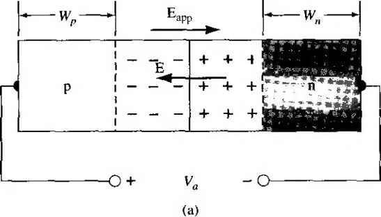 Figure 8.3 ) (a) A pn junction with an applied forward-bias voltage showing the direcfions of the electric field induced by Va and the space charge electric field, (b) Energy-band diagram of the forward-biased pn junction. achieved at thermal equilibrium is upset. The electric field force that prevented majority carriers from crossing the space charge region is reduced; majority carrier electrons from the n side are now injected across the depletion region into the p material, and majority carrier holes from the p side are injected across the depletion region into the n material. As long as the bias V is applied, the injection of carriers across the space charge region conrinues and a current is created in the pn junction. This bias condition is known as forward bias; the energy-band diagram of the forward-biased pn junction is shown in Figure 8.3b. The potential barrier Vtj in Equation (8.4) can be replaced by (V/ - V) when the juncrion is forward biased. Equation (8.4) becomes Пр= л„о exp -е(Уы - Уд) кТ Ппо exp -еУы кТ ехр (8-5) If we assume low injection, the majority carrier electron concentration о* for example, does not change significantly. However, the minority carrier concentration, tip, can deviate from its thermal-equilibrium value Про by orders of magnitude. Using Equation (8.4), we can write Equation (8.5) as 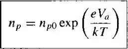 (8.6) When a forward-bias voltage is applied to the pn juncrion, the juncrion is no longer in thermal equilibrium. The left side of Equation (8.6) is the total minority carrier electron concentration in the p region, which is now greater than the thermal equilibrium value. The forward-bias voltage lowers the potenrial barrier so that majority carrier electrons from the n region are injected across the junction into the p region, thereby increasing the minority carrier electron concentration. We have produced excess . minority carrier electrons in the p region. \ When the electrons are injected into the p region, these excess carriers are subject to the diffusion and recombination processes we discussed in Chapter 6. Equation (8.6), then, is the expression for the minority carrier electron concentration at the j edge of the space charge region in the p region. Exactiy the same process occurs for majority carrier holes in the p region which are injected across the space charge region into the n region under a forward-bias voltage. We can write that Pn = Pno exp (8-7) where is the concentration of minority carrier holes at the edge of the space charge region in the n region. Figure 8.4 shows these results. By applying a forward-bias voltage, we create excess minority carriers in each region of the pn junction. Hole injection eV If Fleetron injection = 0 X. Figure 8.4 I Excess minority carrier concentrations al the space charge edges generated by the forward-bias voUage, EXAMPLE 8.1 Objective To calculate the minority carrier hole concentration at the edge of the space charge region of a pn junction when a forward bias is applied. Consider a silicon pn junction at Г = 300 К so that /7, = L5 x 10 cm I Assume the n-type doping is 1 x 10 cm~ and assume that a forward bias of 0,60 V is applied to the pn junction. Calculate the minority carrier hole concentration at the edge of the space charge region. Solution From Equation (8.7) we have p = Pno exp I 1 The thermal-equilibrium minority carrier hole concentration is (1.5 X 10) = 2.25 X 10 cm We then have p =2.25 x lOexpf ) v-0259/ 2.59 x 10 cm Comment The minority carrier concentrahon can increase by many orders of magnitude when a forward-1 bias voltage is applied. Low injection still applies, however, since the excess-electron concentration (equal to the excess-hole concentration in order to maintain charge neutrality) is much less than the thermal-equilibrium electron concentration. TEST YOUR UNDERSTANDING E8.1 A silicon pn junction at 7 = 300 К is doped with impurity concentrations of iVj = 5 x 10 cm~ andiV = 2 x 10 cm~\The junction is forward biased at V 0.610 V. fO {x<xp) (8.10) where i.; = Д,т„о. Determine the minority carrier concentrations at the space charge edges. li rfil X 06f С'х-)г^\тэ .,of > Z9L = VYd suyj E8.2 The impurity doping concentrations in a silicon pn jiinction qkT = 300 К arc /Vj = 5 X 10- cm~ and Л^ 5 x 10 cm-\ The minority carrier concentration at either space charge edge is to be no larger than J 0 percent of the respective majority carrier concentration. Calculate the maximum forward bias voltage that can be applied to this junction and still meet the required specifications. [Л 66£;*0 = (tni)V\ suy] E8.3 Repeat E8.2 for a GaAs pn junction with the same doping concentrations. [AL90T (хрш) д -suvl The minority carrier concentrations at the space charge edges, given by Equations (8.6) and (8.7), were derived assuming a forward-bias voltage (V, > 0) was applied across the pn junction. However, nothing in the derivation prevents from being negative (reverse bias). If a reverse-bias voltage greater than a few tenths of a volt is applied to the pn junction, then we see from Equations (8.6) and (8.7) that the minority carrier concentrations at the space charge edge are essenrially zero. The minority canrier concentrations for the reverse-bias condition drop below the thermal-equilibrium values. 8.1,4 Minority Carrier Distribution We developed, in Chapter 6, the ambipolar transport equation for excess minority carrier holes in an n region. This equarion, in one dimension, is dJC- dx Tpo ot where Ьрп - Pn - PnO is the excess minority carrier hole concentrarion and is the difference between the total and thermal equilibrium minority carrier concentrations. The ambipolar transport equation describes the behavior of excess carriers as a tunc-tion of rime and spatial coordinates. In Chapter 5, we calculated drift current densities in a semiconductor. We deter-in ined that relatively large currents could be created with fairly small electric fields. As a first approximation, we will assume that the electric field is zero in both the neutral p and n regions. In the n region for .v > x , we have that E = 0 and g - 0. If we also assume steady state so d{Sp,j)/Bt 0, then Equation (8.8) reduces to where - ОрГрц. For the same set of conditions, the excess minority carrier electron concentration in the p region is determined from The boundary conditions for the total minority carrier concentrations are РпЫ = /7 о exp Пр{~Хр) = Про exp p (x +00) = Пр{х -00) = PnO rtpO (8.1 h (8.111 (8ЛЬ (8.U( As minority carriers diffuse from the space charge edge into the neutral semicond tor regions, they will recombine with majority carriers. We will assume that lengths W and Wp shown in Figure 8.3a are very long, meaning in particular W :s> Lp and Wp L . The excess minority carrier concentrations must appro zero at distances far from the space charge region. The structure is referred to as long pn junction. The general solution to Equation (8.9) is 8p,{x) = рЛх) - PnO Ле + Be-r (x > x) (8.12 and the general solution to Equation (8.10) is Sripix) = Пр(х) (8ЛЗ) Applying the boundary conditions from Equations (8.11c) and (8. lid), the coefficients Л and D must be zero. The coefficients В and С may be determined from the boundary conditions given by Equations (8. И a) and (8.1 lb). The excess carrier concentrations are then found to be, for (jc > x ).
(8.14) (8 Л 5) The minority carrier concentrarions decay exponentially with distance away from the junction to their thermal-equilibrium values. Figure 8.5 shows these results. Again, we have assumed that both the n-region and the p-region lengths are long compared to the minority carrier diffusion lengths. To review, a forward-bias voltage lowers the built-in potential barrier of a pn junction so that electrons from the n region are injected across the space charge region, creating excess minority carriers in the p region. These excess electrons begin diffusing into the bulk p region where they can recombine with majority carrier holes. The excess minority carrier electron concentration then decreases with distance from the junction. The same discussion applies to holes injected across the space charge region into the n region. 8Л .5 Ideal pn Junction Current The approach we use to determine the current in a pn junction is based on the three parts of the fourth assumption stated earlier in this section. The total current in the junction is the sum of the individual electron and hole currents which are constant through the depletion region. Since the electron and hole currents are continuous functions through the pn junction, the total pn junction current will be the minority carrier hole diffusion current at x - jcj plus the minority carrier electron diffusion current at X = -Xp. The gradients in the minority carrier concentrarions, as shown in Figure 8.5, produce diffusion currents, and since we are assuming the electric field to be zero at the space charge edges, we can neglect any minority carrier drift current component. This approach in determining the pn junction current is shown in Figure 8.6. 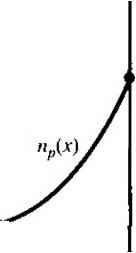 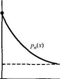 -Xp x = 0 x Figure 8-5 I Steady-state minority carrier concentrations in a pn junction under forward bias. Current t density -Xp X = 0 X Figure 8.6 I Electron and hole current densities through the space charge region of a pn junction. We can calculate the minority carrier hole diffusion current density ax x - from the relation -eD, (8.1( Since we are assuming uniformly doped regions, the thermal-equilibrium came concentration is constant, so the hole diffusion current density may be written as Jp{xn) = -eD, djbpnjx)) dx (8.1 Taking the derivative of Equation (8.14) and substituting into Equation (8.17), obtain The hole current density for this forward*bias condition is in the -\-x direction, whit is from the p to the n region. Similarly, we may calculate the electron diffusion current density x - -Xp\ This may be written as 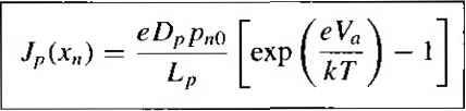 Using Equation (8Л 5), we obtain d{8np{x)) dx (8.l X - -X, (8.: The electron current density is also in the +x direction. An assumption we made at the beginning was that the individual electron and hole cunents were continuous functions and constant through the space charge region. The total current is the sum of the electron and hole currents and is constant throu the entire junction. Figure 8.6 again shows a plot of the magnitudes of these current The total current density in the pn junction is then J = JpiXn) + Jni-Xn) = ~~L-- (8.21X Equation (8.21) is the ideal current-voltage relationship of a pn junction. We may define a parameter Л as eDp PnO О„про ~~L-~r~ 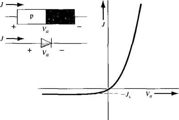 Figure 8.7 Meal /-F characteristic of a pn junction diode. so that Equation (8.21) may be written as 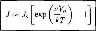 (8.23) \ Equation (8.23), known as the ideal-diode equation, gives a good description of the current-voltage characteristics of the pn junction over a wide range of currents and voltages. Although Equation (8.23) was derived assuming a forward-bias voltage (Ki > 0), there is nothing to prevent from being negative (reverse bias). Equarion (8.23) is plotted in Figure 8.7 as a function of forward-bias voltage V. If the voltage Va becomes negarive (reverse bias) by a few кТ/е V, then the reverse-bias current [ density becomes independent of the reverse-bias voltage. The parameter is then I referred to as the reverse saturation current density. The current-voltage characteristics of the pn juncrion diode are obviously not bilateral. ObjecUve To determine the ideal reverse saturation current density in a silicon pn junction at Г = 300 К. Consider the following parameters in a silicon pn junction: К = N. Д, = 25 cm-Zs Dp = 10 cm/s cm-- т = \.5х 10 cm- V) = t o = 5 X 10 s = 11.7 Solution The ideal reverse saturation current density is given by EXAMPLE 8.2 к 1 ... 25 26 27 28 29 30 31 ... 55 |
||||||||||||
|
© 2026 AutoElektrix.ru
Частичное копирование материалов разрешено при условии активной ссылки |