 |
 |
 |
| Главная Журналы Популярное Audi - почему их так назвали? Как появилась марка Bmw? Откуда появился Lexus? Достижения и устремления Mercedes-Benz Первые модели Chevrolet Электромобиль Nissan Leaf |
Главная » Журналы » Absorbing materialorganic polymer 1 ... 26 27 28 29 30 31 32 ... 55 which nay be rewritten as 1 a 1 /А Na v lO Nd v Substituting the parameters, we obtain = 4Л5 x Ш A/cm. Comment The ideal reverse-bias saturation current density is very small. If the pn junction cross-sectional area were A = 10 * cm, for example, then the ideal reverse-bias diode current would be /, =4Л5 x 10 A. Figure 8.8 I Ideal /-V characteristic of a pn junction diode with the current plotted on a log scale. If the forward-bias voltage in Equation (8.23) is positive by more than a few kT/e\o]is, then the (-1) term in Equation (8.23) becomes negligible. Figure 8.8 shows the forward-bias current-voltage characteristic when the current is plotted on a log scale. Ideally, this plot yields a straight line when V, is greater than a few kT/evo\Xs. The forward-bias current is an exponential function of the forward-bias voltage. DESIGN EXAMPLE 8,3 Objective To design a pn junction diode to produce particular electron and hole current densities at a given forward-bias voltage. Consider a silicon pn junction diode at Г = 300 К. Design the diode such that J =; 20 kicwr and Jp =5 A/cixr at = 0.65 V. Assume the remaining semiconductor paranveters are as given in Example 8.2. Solution The electron diffusion current density is given by Equation (8.20) as Jubstituting the numbers, we have 20=- (1.6 x 10-). 5 x 10 (1.5 x 10 ) 10\2 Г / 0.65 \ /hich yields = 1.01 x 10 cm- hole diffusion current density is given by Equation (8.18) as .2 Г Substituting the numbers, we have 5 = (1.6 x 10~) 5 x 10 (1.5 x 10) i0\2 Г 0.65 \ ! which yields iVj = 2.55 x 10 cm- Comment \ The relative magnitude of the electron and hole current densities through a diode can be varied by changing the doping concentrations in the device. TEST YOUR UNDERSTANDING E8.4 A silicon pn junction at T = 300 К has the following parameters: =5 x 10 cm -\ iVrf = 1 x 10 cm--\ D = 25 cm/s. Dp = 10 cm/s, г„о = 5 x 10 s, and = 1 x 10~ s. The cross-sectional area is Л = lO * cm-and the forward-bias voltage is Va = 0.625 V. Calculate the (a) minority electron diffusion current at the space charge edge, (h) minority hole diffusion current at the space charge edge, and (c) total current in the pn junction diode. [V pfl () 60 I (Я) iil *0 () suyl E8.5 Repeat E8.4 for a GaAs pn junction diode biased at V = 1.10 V. [уш 59-1 (0) Vnt PY\ (q) tOO () suvl 8.1,6 Summary of Physics We have been considering the case of a forward-bias voltage being applied to a pn junction. The forward-bias voltage lowers the potential barrier so that electrons and holes are injected across the space charge region. The injected carriers become minofl ity carriers which then diffuse from the junction and recombine with majority carriers We calculated the minority carrier diffusion current densities at the edge of space charge region. We can reconsider Equations (8.14) and (8.15) and deter the minority carrier diffusion current densities as a function of distance through p- and n-regions. These results are  Jp(x) = m - ] (X > Xn) (8.24) 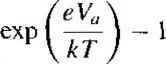 (X < -Xp) (8.25) The minority carrier diffusion current densities decay exponentially in each region. However, the total current through the pn junction is constant. The difference between total current and minority carrier diffusion current is a majority carrier current. Figure 8.9 shows the various current components through the pn structure. The drift of majority earner holes in the p region far from the junction, for example, is to supply holes that are being injected across the space charge region into the n region and also to supply holes that are lost by recombination with excess minority carrier electrons. The same discussion applies to the drift of electrons in the n region. We have seen that excess carriers are created in a forward-biased pn junction. From the results of the ambipolar transport theory derived in Chapter 6, the behavior of the excess carriers is determined by the minority carrier parameters for low injec-rion. In determining the current-voltage relationship of the pn junction, we consider the flow of minority carriers since we know the behavior and characteristics of these Current f Majority carrier hole current Electron diffusion current
Majority carrier electron current Hole diffusion current -x л - 0 x Figure 8.9 I Ideal electron and hole current components through a pn junction under forward bias. particles. It may seem strange, at times, that we concern ourselves so much with minority carriers rather than with the vast number of majority carriers, but the reason for this can be found in the results derived from the ambipolar transport theory. TEST YOUR UNDERSTANDING E8,6 Consider the sihcon pn junction diode described in E8.4. Calculate the electron and hole currents а1{а}х = .v , (/?) jr = jc + LJ, and (c) x = jc + iOLp (see Figure 8.9). [0 V Vtn fpf I = 7 (J): rOt70 V Vtw £fs-0 = 7 tyni 604 = I Viu pgro = 7 ( ) suvl The fact that we now have drift current densities in the p and n regions implies that the electric field in these regions is not zero as we had originally assumed. We can calculate the electric field in the neutral regions and determine the vahdity of our zero-field approximarion. Objective To calculate the electric field required to produce a given majority carrier drift current. Consider a silicon pn junction at T = 300 К with the parameters given in Example 8.2 and with an applied forward-bias voltage = 0.65 V. Solution The total forward-bias current density is given by J = Л We determined the reverse saturation current density in Example 8.2, so we can write J = (4.15 x 10 ) 0.65 \ 0259 = 3.29 A/cm total current far from the junction in the n-region will be majorhy carrier electron drift current, so we can write J Jn eptjNdE The doping concentration is Л^ = 10 cm , and, if we assume Pn = 1350 cm /V-s, then the electric field must be Л 3.29 efiNj (1.6 X 10 9)(1350)(10й) = 1.52 V/cm Comment f We assumed, in the derivation of the current-voltage equation, that the electric field in the neu- tral p and n regions was zero. Although the electric field is not zero, this example shows that ., the magnitude is very small-thus the approximation of zero electric field is very good. EXAMPLE 8.4 8Л -7 Temperature Effects The ideal reverse saturation current density Js, given by Equation (8.22), is a functic of the thermal-equilibrium minority carrier concentrations Про and p o- These minors ity carrier concentrations are proportional to ?, which is a very strong function temperature. For a silicon pn junction, the ideal reverse saturation current density increase by approximately a factor of four for every 10 С increase in temperature. The forward-bias current-voltage relation was given by Equation (8.23). relation includes Л as well as the cxieVa/kT) factor, making the forward-bii current-voltage relation a function of temperature also. As temperature increases, les forward-bias voltage is required to obtain the same diode current. If the voltage ishek constant, the diode current will increase as temperature increases. The change in forward-bias current with temperature is less sensitive than the reverse saturation currei EXAMPLE 8,5 Objective To determine the change in the forward-bias voltage on a pn junction with a change in tem-i perature. Consider a silicon pn junction initially biased at 0.60 V at Г = 300 К. Assume the temperature increases to Г = 310 K. Calculate the change in the forward-bias voltage required to maintain a constant current through the junction. Solution The forward-bias current can be written as follows: oc exp exp {-) If the temperature changes, we may take the ratio of the diode currents at the two temperatures. This ratio is h ехр(-£:Г2)ехр(еУ2/Г2) 7] txp(-Ef,/kTi) exp (e Va\/kT]) If current is to be held constant, then J = J2 and we must have Eg - eVa2 Eg - eVgX Let Ti = 300K, Г2 = 310 K, E = 1.12 eV, and Va\ = 0.60 V Then, solving for V2. we obtain V2 = 0.5827 V Comment The change in the forward-bias voltage is -17.3 mV for a 10°C temperature change. 8.L8 The Short Diode We assumed in the previous analysis that both p and n regions were long compared with the minority carrier diffusion lengths. In many pn junction structures, one region 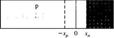 Figure 8.101 Geometry of a short diode. 1лау, in fact, be short coiupared with the minority carrier diffusion length. Figure 8.10 shows one such example: the length W is assumed to be much smaller than the minority carrier hole diffusion length, Lp. The steady-state excess minority carrier hole concentration in the n region is determined from Equation (8.9), which was given as The original boundary condition at x = x still applies, given by Equation (8.lla) as Pn(Xn) = Ajo exp A second boundary condition needs to be determined. In many cases we will assume that an ohmic contact exists at лс = (x + VK ), implying an infinite surface-recombination velocity and therefore an excess minority carrier concentration of zero. The second boundary condition is then written as PnU = + Л10 (8.26) The general solution to Equation (8.9) is again given by Equation (8.12), which was i BpnM = PnM - Pnu - Ae + Be- * (x > x,) In this case, because of the finite length of the n region, both terms of the general solution must be retained. Applying the boundary conditions of Equations (8.1 lb) and (8.26), the excess minority carrier concentration is given by %з() = PnO sinhKx;, 4- ty -x)/Lp] sinh[ty /p] (8-27) Equation (8-27) is the general solution for the excess minority carrier hole concentration in the n region of a forward-biased pn junction. If Wi Lp the assumption for the long diode, Equation (8.27) reduces to the previous result given by Equation (8.14). If <$С L we can approximate the hyperbolic sine terms by sinh( + --)(: + w (8.28a) sinh I -- I (8.28 Then Equation (8.27) becomes  (8.2 The minority carrier concentration becomes a hnear function of distance. The minority carrier hole diffusion current density is given by Jp = -eDp so that in the short n region, we have eDpPno Jn(x) The minority carrier hole diffusion current density now contains the length iV in denominator, rather than the diffusion length Lp. The diffusion current density is largt for a short diode than for a long diode since W < Lp. In addition, since the minority! carrier concentration is approximately a linear function of distance through the n region, the minority carrier diffusion current density is a constant. This constant current implies that there is no recombination of minority carriers in the short region. TEST YOUR UNDERSTANDING E8.7 Consider the silicon pn junction diode described in E8.4- The p region is long and the n region is short with W 2 дт. (a) Calculate the electron and hole currents in the depletion region, (h) Why has the hole current increased compared to that found in E8.4? [p9SF9J3ui snq jUQiptJjS Xiisu9p о\щ Щ1 {q) tyui руд = V P\0= I W uy] 8.2 I SMALL-SIGNAL MODEL OF THE , pn JUNCTION We have been considering the dc characteristics of the pn junction diode. When semiconductor devices with pn junctions are used in linear amplifier circuits, for example, sinusoidal signals are superimposed on the dc currents and voltages, so that the small-signal characteristics of the pn junction become important. 8.2.1 Diffusion Resistance The ideal cunent-voltage relationship of the pn junction diode was given by Equation (8.23), where J and Л are current densities. If we multiply both sides of the 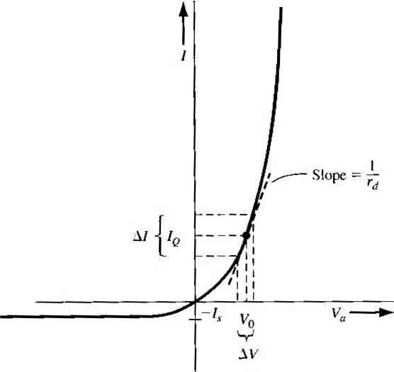 Figure 8.11 I Curve showing the concept of the small-signal diffusion resistance. equation by the junction cross-sectional area, we have Id = h (8.31) where Id is the diode current and h is the diode reverse saturation current. Assume that the diode is forward-biased with a dc voltage Vq producing a dc diode current Ioq If we now superimpose a small, low-frequency sinusoidal voltage as shown in Figure 8. П, then a small sinusoidal current will be produced, superimposed on the dc current. The ratio of sinusoidal current to sinusoidal voltage is called the incremental conductance. In the limit of a very small sinusoidal current and voltage, the small-signal incremental conductance is just the slope of the dc current-voltage curve, or (8.32) The reciprocal of the incremental conductance is the incremental resistance, defined as (833) where Ioq is the dc quiescent diode current. If we assume tiiat the diode is biased sufficientiy far in the forward-bias region, then the (-1) term can be neglected and the incremental conductance becomes gd = K,=Vo (8.34) The small-signal incremental resistance is then the reciprocal function, or 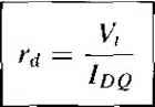 (8.35) The incrennental resistance decreases as the bias current increases, and is inversely proportional to the slope of the I-V characteristic as shown in Figure 8.1 F The incremental resistance is also known as the diffusion resistance, 8.2.2 Small-Signai Admittance In the last chapter, we considered the pn junction capacitance as a function of reverse-bias voltage. When the pn junction diode is forward-biased, another capacij tance becomes a factor in the diode admittance. The small-signal admittance, or pedance, of the pn junction under forward bias is derived using the minority camt diffusion current relations we have already considered. Qualitative Analysis Before we delve into the mathematical analysis, we can quali itatively understand the physical processes that lead to a diffusion capacitance, whici is one component of the junction admittance. Figure 8.12a schemarically shows ц pn junction forward biased with a dc voltage. A small ac voltage is also superimposet on the dc vohage so that the total forward-biased voltage can be written К = Vdc + sin cot, As the voltage across the junction changes, the number of holes injected acn the space charge region into the n region also changes. Figure 8.12b shows the hoi concentration at the space charge edge as a function of time. At f = t(u the ac voU 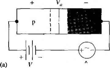 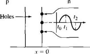 Time PnOexp 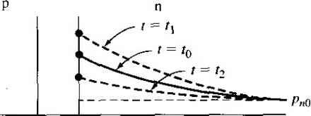 x = 0 Figure 8Л2 I (a) A pn junction with an ac voltage superimposed on a forward-biased dc value; (b) the hole concentration versus time at the space charge edge; (c) the hole concentration versus distance in the n region at three different times. is zero so that the concentration of holes at x = 0 is just given by p (0) /V) exp (Vjc/ K), which is what we have seen previously. Now, as the ac voltage increases during its positive half cycle, the concentration of holes at jc = 0 will increase and reach a peak value att - t], which corresponds to the peak value of the ac voltage. When the ac voltage is on its negative half cycle, the total voltage across the junction decreases so that the concentration of holes at л - 0 decreases. The concentration reaches a minimum value at r = Г2, which corresponds to the time that the ac voltage reaches its maximum negative value. The minority carrier hole concentration at x - 0, then, has an ac component superimposed on the dc value as indicated in Figure 8T2b. As previously discussed, the holes at the space charge edge (x = 0) diffuse into the n region where they recombine with the majority carrier electrons. We will assume that the period of the ac voltage is large compared to the time it takes carriers to diffuse into the n region. The hole concentration as a function of distance into the n region can then be treated as a steady-state distribution. Figure 8.12c shows the steady-state hole concentrations at three different times. At r = to, the ac voltage is zero, so the t = to curve corresponds to the hole distribution established by the dc voltage. The / = 1 curve corresponds to the distriburion established when the ac voltage has reached its peak positive value, and the t - t2 curve corresponds to the distribution established when the ac voltage has reached its maximum negative value. The shaded areas represents the charge Д Q that is alternately charged and discharged during the ac voltage cycle. Exactly the same process is occurring in the p region with the electron concentration. The mechanism of charging and discharging of holes in the n region and electrons in the p region leads to a capacitance. This capacitance is called diffusion capacitance. The physical mechanism of this diffusion capacitance is different from that of the junction capacitance discussed in the last chapter. We will show that the magnitude of the diffusion capacitance in a forward-biased pn junction is usually substantially larger than the junction capacitance. Mathematical Analysis The minority carrier distribution in the pn junction will be derived for the case when a small sinusoidal voltage is superimposed on the dc juncrion voltage. We can then determine small signal, or ac, diffusion currents from these minority carrier functions. Figure 8.13 shows the minority carrier distribution in a pn junction when a forward-biased dc voltage is applied. The origin, x = 0, is set at the edge of the space charge region on the n-side for convenience. The minority carrier hole concentration at x -0 is given by Equation (8.7) as /? (0) = pfjQ exp (eVa/kT), where K is the applied voltage across the junction. Now let V, = Vo + l(0 (8.36) where Vo is the dc quiescent bias voltage and V\(t) is the ac signal voltage which is superimposed on this dc level. We may now write Pn (x = 0) p o exp e(Vo + vi{t)) kT = Pn(0,t) (8.37) 1 ... 26 27 28 29 30 31 32 ... 55 |
|||||||||||||||||||||||||||
|
© 2026 AutoElektrix.ru
Частичное копирование материалов разрешено при условии активной ссылки |