 |
 |
 |
| Главная Журналы Популярное Audi - почему их так назвали? Как появилась марка Bmw? Откуда появился Lexus? Достижения и устремления Mercedes-Benz Первые модели Chevrolet Электромобиль Nissan Leaf |
Главная » Журналы » Absorbing materialorganic polymer 1 ... 27 28 29 30 31 32 33 ... 55 Пы\--. 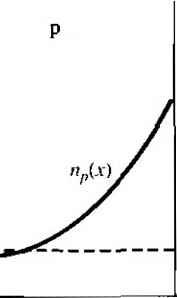 = Pna exp 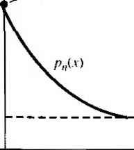 Vkr\ л = 0 Figure 8.13 I The dc characteristics of a forward-biased pn junction used in the small-signal admittance calculations. Equation (8.37) may be written as where / ev](t) РпФ. 0 = Pdc expl Pdc = PnO exp (8.31 (8.3! If we assume that \vi(t)\ < (кТ/е) = VJ, then the exponential term in Equation (8.38) may be expanded into a Taylor series retaining only the linear terms, the minority carrier hole concentration at x = 0 can be written as (8> If we assume that the time-varying voltage ii(/) is a sinusoidal signal, we can] write Equation (8.40) as where V] is the phasor of the applied sinusoidal voltage. Equation (8.41) will be used as the boundary condition in the solution of the time-dependent diffusion equation for the minority carrier holes in the n region. In the neutral n region (jc > 0), the electric field is assumed to be zero, thus the behavior of the excess minority carrier holes is determined from the equation diSp ) 8pn S(8p ) (8.42) where 8pn is the excess hole concentration in the n region. We are assuming that the ac signal voltage v\(t) is sinusoidal. We then expect the steady-state solution for 5p to be of the form of a sinusoidal solution superimposed on the dc solution, or 8pAx,t)8poix) + p,ix)e (843) where 5po{x) is the dc excess carrier concentration and /?i (.v) is the magnitude of the ac component of the excess carrier concentration. The expression for Spoix) is the same as that given in Equation (8.14). Substituting Equation (8.43) into the differential Equation (8.42), we obtain S(Spo(x)) dpi(x) j dx- dx PoCv) + Pi() = j(P\{x)e (8.44) We may rewrite this equation, combining the time-dependent and time-independent terms, as a(%)(x)) SpoixY -jo)pi(x) jO)l (8.45) If the ac component, piix), is zero, then the first bracketed term is just the differential Equation (8. JO), which is identically zero. Then we have, from the second bracketed term. - j(op\(x) = 0 looting that L, = Equation (8.46) may be rewritten in the form pdx)=0 (8.46) (8.47) dp\(x) dx- CIp,(x)=Q where 2 (1 + jgjrx)) The general solution to Equation (8.48) is (8.48) (8.49) (8.50) One boundary condition is that /?] (x +oc) = 0, which implies that the coefficient K2 = 0. Then P{(x) = Kie (8.51) Applying the boundary condititm at x - 0 from Equation (8.41) we obtain pi(0) = ATi = Ale (8.52) The hole diffusion current density can be calculated at л =0. This will be giv (8.53) x = 0 If we consider a homogeneous semiconductor, the derivative of the hole concentration will be just the derivative of the excess hole concentration. Then = -cD, x = 0 x = 0 dx We can write this equation in the form = JpO -b jpU) dpi (x) (8.54) (8.55) where BjSpoix)) dx exp I - I - 1 (8.56) Equation (8.56) is the dc component of the hole diffusion current density and is exactly the same as in the ideal /-V relation derived previously. The sinusoidal component of the diffusion current density is then found from dpi(jO dx (8.57)
where Jp is the current density phasor. Combining Equations (8.57), (8.51), and (8.52), we have Jp -eOpi-Cp) (8.58) We can write the total ac hole current phasor as ip -- AJp eADpCpP, (8.59) where A is the cross-sectional area of the pn junction. Substituting the expression for Cp, we obtain P eADpPdc rr---- (8.60) If we define eADpP (8.61) then Equation (8.60) becomes We can go through the same type of analysis for the minority carrier electrons in the p region. We will obtain where fnO - (8.63) (8.64) The total ac current phasor is the sum of , and / . The pn junction admittance is the total ac current phasor divided by the ac voltage phasor, or / + / / 1 \ г /-- у-~- (8.65) There is not a linear, lumped, finite, passive, bilateral network that can be synthesized to give this admittance funcrion. However, we may make the following approximations. Assume that ОУТрО < 1 (8.66a) <УТ о < 1 (8.66b) These two assumptions imply that the frequency of the ac signal is not too large. Then we may write (8.67a) yj 1 -h 7 tt>r o 1 + (8.67b) Substituting Equations (8.67a) and (8.67b) into the admittance Equarion (8.65) yields (8.68) If we combine the real and imaginary portions, we get ( 70 + / o) + Jo) (8.69) Equation (8.69) may be written in the form p region ГФ) = Pm exp 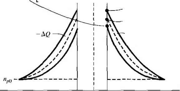 n region ЛДО) = p o exp - Pni) Figure 8.14 I Minority carrier concentration ctiangcs with changing forward-bias voltage. The parameter is called the diffusion conductance and is given by gd - j У'рО -г / оу - yo,i where Ioq is the dc bias current. Equation (8.71) is exactly the same conductance we obtained previously in Equation (8.34). The parameter is called the diffusU capacitance and is given by (/,0 + Аю) = (8.71) usiofu 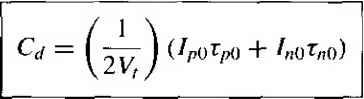 (8.72) The physics of the diffusion capacitance may be seen in Figure 8.14. The dc values of the minority carrier concentrations are shown along with the changes due to the ac component of voltage. The Д Q charge is alternately being charged and discharged through the junction as the voltage across the junction changes. The change in the stored minority carrier charge as a function of the change in voltage is the diffusion capacitance. One consequence of the approximations шго 1 and о>т^о < 1 is that there are no wiggles in the minority carrier curves. The sinusoidal frequency is low enough so that the exponential curves are maintained at all times. EXAMPLE 8.6 Objective To calculate the small-signal admittance of a pn junction diode. This example is intended to give an indication of the magnitude of the diffusion capacitance as compared with the junction capacitance considered in the last chapter. The diffusion resistance will also be calculated. Assume that Nj so that p o px> This assumpiton implies that ,(> > / o- Let T = 300 K, tq = \0~ s, and /,0 = Ioq = 1 niA. Solution The diffusion capacitance, with these assumptions, is given by 10-)(10-) = 1.93 X 10 F The diffusion resistance is V, 0.0259 V - =---- 25.9 12 Ioq 1mA Comment The value of J.93 nF for the diffusion capachance of a forward-biased pn junction is 3 to 4 orders of magnitude larger than the junction capacitance of the reverse-biased pn junction, which we calculated in Example 7.5. The diffusion capacitance tends to dominate the capacitance terms in a forward-biased pn junction. The small-signal diffusion resistance can be fairly small if the diode current is a fairly large value. As the diode current decreases, the diffusion resistance increases. We will consider the impedance of forward-biased pn junctions again when we discuss bipolar transistors. TEST YOUR UNDERSTANDING E8.8 A silicon pn junction diode at T = 300 К has the following parameters: = 8 x 10 cm--\ N,=2x 10 cm-\D = 25 cmVs, = 10 cmVs, r,o = 5x 10 s, and Xpo = \0~ s. The cross-sectional area is Л = 10 cm. Determine the diffusion resistance and diffusion capacitance if the diode is forward biased at (a) = 0.550 V and Ф) Va =0.610 V. № вЖ = о 9 11 = (Ф - ju LOZ =0*811 = *suVl E8.9 A GaAs pn junction diode at T = 300 К has the same parameters given in E8.8 except that D = 207 cm/s and Dp =9.80 cm/s. Determine the diffusion resistance and diffusion capacitance if the diode is forward biased at (й) Va = 0.970 V and (b)Va = 1.045 V. lJu OYI = Ъ 9V\ = -Ju 0t6 0 = £9Z = - () Vl 8.2.3 Equivalent Circuit The small-signal equivalent circuit of the forward-biased pn junction is derived from Equation (8.70). This circuit is shown in Figure 8.15a. We need to add the junction capacitance, which will be in parallel with the diffusion resistance and diffusion capac- itance. The last element we add, to complete the equivalent circuit, is a series resistance. The neutral n and p regions have finite resistances so the actual pn junction will include a series resistance. The complete equivalent circuit is given in Figure 8.15b. The voltage across the actual junction is Va and the total voltage applied to .the pn diode is given by Vapp The junction voltage Va is the voltage in the ideal 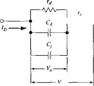 Figure 8Л51 (a) Small-signal equivalent circuit of ideal forward-biased pn junction diode; (b) Complete small-signal equivalent circuit of pn junction. Effect of 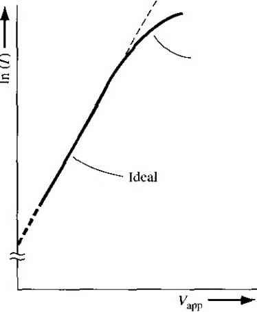 Figure 8Л61 Forward-biased /-V characteristics of a pn junction diode showing the effect of series resistance. current-voltage expression. We can write the expression (8.73) Figure 8 Л 6 is a plot of the current-voltage characteristic fronn Equation (8.73) showing the effect of the series resistance. A larger applied voltage is required to achieve the same current value when a series resistance is included. In most diodes, the series resistance will be negligible. In some semiconductor devices with pn junctions, however, the series resistance will be in a feedback loop; in these cases, the resistance is multiplied by a gain factor and becomes non-negligible. TEST YOUR UNDERSTANDING E8.10 A silicon pn junction diode at Г = 300 К has the same parameters as those described in E8.8, The neutral n-region and neutral p-region lengths are 0.01 cm. Estimate the scries resistance of the diode (neglect ohmic contacts). (13 99 = N suy) 8.3 I GENERATION-RECOMBINATION CURRENTS In the derivation of the ideal current-voltage relationship, we neglected any effects * occurring within the space charge region. Since other current components are generated within the space charge region, the actual I-V characterisrics of a pn junction diode deviate from the ideal expression. The additional currents are generated from the recombination processes discussed in Chapter 6. The recombinarion rate of excess electrons and holes, given by the Shockley-Read-Hall recombination theory, was written as C,jC Nf{np - n;) R -r \ r-,J- I The parameters n and p are, as usual, the concentrations of electrons and holes, spectively. ,ЗЛ Reverse-Bias Generation Current For a pn junction under reverse bias, we have argued that the mobile electrons and holes have essentially been swept out of the space charge region. Accordingly, within [the space charge region, n p 0, The recombination rate from Equarion (8.74) ;omes -Cy,CnNtn.f R = (8.75) C,n + Cpp The negative sign implies a negative recombination rate; hence, we are really generating electron-hole pairs within the reverse-biased space charge region. The recombination of excess electrons and holes is the process whereby we are trying to reestablish thermal equilibrium. Since the concentration of electrons and holes is essentially zero within the reverse-biased space charge region, electrons and holes are being generated via the trap level to also try to reestablish thermal equilibrium. This generation process is schematically shown in Figure 8.17. As the electrons and holes are generated, they are swept out of the space charge region by the electric field. The flow of charge is in the direction of a reverse-bias current. This reverse-bias generation current, caused by the generation of electrons and holes in the space charge region, is in addition to the ideal reverse-bias saturation current. We may calculate the density of the reverse-bias generation current by considering Equation (8.75). If we make a simplifying assumption and let the trap level be at the intrinsic Fermi level, then from Equations (6.92) and (6.97), we have that n = л,- E-held 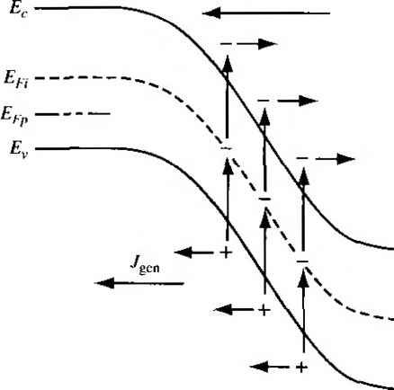 -£c ----Efi Figure 8.17 I Generation process in a reverse-biased pn junction. and p = Equation (8.75) now becomes NrCp NrC, (8.7( Using the definitions of lifetimes from Equations (6.103) and (6.104), we may writ< Equation (8.76) as rii TpO + r o If we define a new lifetime as the average of Гро and r o, or XpQ + r o then the recombination rate can be written as (8.78) R--G 2to (8.7< The negative recombination rate implies a generation rate, so G is the generation rate of electrons and holes in the space charge region. The generation current density in ay be determined from eG dx (8.80) where the integral is over the space charge region. If we assume that the generation rate is constant throughout the sptice charge region, then we obtain 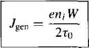 (8.81) The total reverse-bias current density is the sum of the ideal reverse saturation current density and the generation current density, or Л + 4 (8.82) The ideal reverse saturation current density Л is independent of the reverse-bias voltage. However, is a function of the depletion width tV, which in turn is a function of the reverse-bias voltage. The actual reverse-bias current density, then, is no longer independent of the reverse-bias voltage. I Objective To determine the relative magnitudes of the ideal reverse saturation current density and the generation current density in a silicon pn junction at T = 300 K. Consider the sihcon pn junction described in Example 8.2 and Jet Tq = Zpo г,о = 5 x Ш- s. Solution The ideal reverse saturation current density was calculated in Example 8.2 and was found to be Л = 4.15 x 10 A/cnr. The generation current density is again given by Equation (8.81) eni W 2t{) and the depletion width is given by 26, (KNd If we assume, for example, that Уы Ч- = 5 V, then using the parameters given in Example 8.2 we find that IV = 1.14 x 10 * cm, and then calculate the generation current density to be Jgcn =2.74 x 10 A/cm- Comment Coinparing the solutions for the two current densities, it is obvious that, for the silicon pn junction diode at room temperature, the generation current density is approximately four orders of magnitude larger than the ideal saturation current density. The generation current is the dominant reverse-bias current in a silicon pn junction diode. EXAMPLE 8.7 1 ... 27 28 29 30 31 32 33 ... 55 |
|
© 2026 AutoElektrix.ru
Частичное копирование материалов разрешено при условии активной ссылки |