 |
 |
 |
| Главная Журналы Популярное Audi - почему их так назвали? Как появилась марка Bmw? Откуда появился Lexus? Достижения и устремления Mercedes-Benz Первые модели Chevrolet Электромобиль Nissan Leaf |
Главная » Журналы » Absorbing materialorganic polymer 1 ... 28 29 30 31 32 33 34 ... 55 TEST YOUR UNDERSTANDING Е8Л1 A GaAs pn junction diode has the same parameters as described in E8.9. (a) Calculate the reverse-bias generation current if the diode is reverse biased at K/? = 5 V. (b) Determine the ratio of /gen calculated in part (a) to the ideal reverse-saturation current /s- [i Ql X £6*1 Й) V t-Ol x eOT = H suv] 8.3,2 Forward-Bias Recombination Current For the reverse-biased pn junction, electrons and holes are essentially completel; svept out of the space charge region so that n p 0. Under forward bias, how ever, electrons and holes are injected across the space charge region, so we do, i] fact, have some excess carriers in the space charge region. The possibility exists some of these electrons and holes will recombine within the space charge region not become part of the minority carrier distribution. The recombinarion rate of electrons and holes is again given from Equ tion (8.74) as C,{n+n)-hCp(pp) Dividing both numerator and denominator by CnCpNt and using the definitions о T o and Tpo, we may write the recombination rate as \ np - nf Tpo(n -h n) + r o(/7 + p) (8.1 Figure 8.18 shows the energy-band diagram of the forward-biased pn junctic Shown in the figure are the intrinsic Fermi level and the quasi-Fermi levels foj 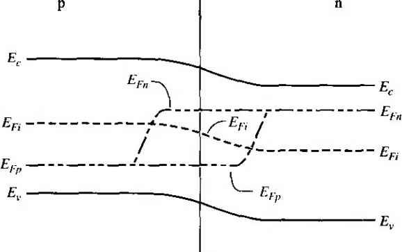 Figure 8Л81 Energy-band diagram of a forward-biased pn junction including quasi-Fermi levels. electrons and holes. From the results of Chapter 6, we may write the electron concentration as n = exp Fn (8.84) and the hole concentration as p - Hi exp Efi - E (8.85) where Efu and Efp are the quasi-Fermi levels for electrons and holes, respectively. From Figure 8.18, we may note that {EFn - Ef,) -h (Efi - Efp) = eV (8.86) where is the applied forward-bias voltage. Again, if we assume that the trap level is at the intrinsic Fermi level, then n = p = n Figure 8.19 shows a plot of the relative magnitude of the recombination rate as a function of distance through the space charge region. This plot was generated using Equations (8.83), (8.84), (8.85), and (8.86). A very sharp peak occurs at the metallurgical junction (x = 0). At the center of the space charge region, we have Efi - (8.87) Relative A Tecombination rate 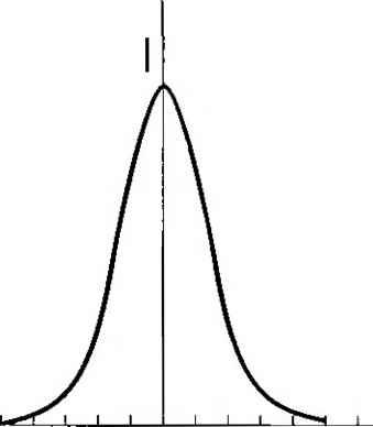 -6 -5 -4 -3-2 -10 1 2 3 4 5 6 Relative distance ttiroijgh space charge region Figure 8.19 I Relative magnitude of the recombination rate through the space charge region of a forward-biased pn junction. Equations (8.84) and (8.85) then become n - fij exp 2k T  (8.89) If we assume that n - p = and that т„о - = tq, then Equation (8.83) becomes fU [ехр(еК, :П-1] (8.90) 2to [exp(V /2r)+ 1] which is the maximum recombination rate for electrons and holes that occurs at tl center of the forward-biased pn junction. If we assume that V, кТ/е, we maj neglect the (-1) term in the numerator and the (+1) term in the denomii Equation (8.90) then becomes 2го \2кТ The recombination current density may be calculated from Лес I eR Jo (8.92) where again the integral is over the entire space charge region. In this case, however, the recombination rate is not a constant through the space charge region. We have calculated the maximum recombination rate at the center of the space charge region, so we may write i/fec - X (8.93) where л' is a length over which the maximum recombination rate is effective. However, since to may not be a well-defined or known parameter, it is customary to write (8.94 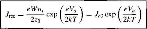 where W is the space charge width. TEST YOUR UNDERSTANDING Е8Л2 Consider a silicon pn junction diode at Г = 300 К with the same parameters given in E8.8. The diode is forward biased at l/ = 0.50 V. (й) Calculate the forward-biased recombination current, (h) Detennine the ratio of /ret.- calculated in part (a) to the ideal diffusion current. [-01 x ]ZL () у 01 x qVZ = 7 () Vl Recom bination 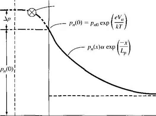 Figure 8.20 I Because of recombination, additional holes from the p region must be injected into the space charge region to cstabHsh the minority carrier hole concentration in the n region. 8.3.3 Total Forward-Bias Current The total forward-bias current density in the pn junction is the sum of the recombination and the ideal diffusion current densities. Figure 8.20 shows a plot of the minority carrier hole concentrarion in the neutral n region. This distribution yields the ideal hole diffusion current density and is a function of the minority carrier hole diffusion length and the applied junction voltage. The distribution is established as a result of holes being injected across the space charge region. If, now, some of the injected holes in the space charge region are lost due to recombination, then additional holes must be injected from the p region to make up for this loss. The flow of these additional injected carriers, per unit time, results in the recombination current. This added component is schematically shown in the figure. The total forward-bias current density is the sum of the recombination and the ideal diffusion current densities, so we can write J - Лес + where У^с is given by Equation (8.94) and Jo is given by (8.95) (8.96) The (-1) term in Equation (8.23) has been neglected. The parameter J, is the ideal reverse saturation current density, and from previous discussion, the value of Ло from the recombination current is larger than the value of Jj, In ( го) Г Total current  Reeombinaiion current, J (slope = ) Ideal diffusion current, (siope - 1) Figure 8.21 I Ideal diffusion, recombination, and total current in a forward-biased pn junction. If we take the natural log of Equations (8.94) and (8.96), we obtain In Угес - In (8.97a; In Jo - In + = In Л + (8.97b Figure 8.21 .shows the recombination and diffusion current components plotted on a log current scale as a function of V/ V. The slopes of the two curves are not the same. Also shown in the figure is the total current density-the sum of the two current components. We may notice that, at a low current density, the recombination current dominates, and at a higher current density, the ideal diffusion current dominates. In general, the diode current-voltage relationship may be written as (8.98) where the parameter n is called the ideality factor. For a large forward-bias voltage, 1 when diffusion dominates, and for low forward-bias voltage, н 2 when recombination dominates. There is a transition region where 1 < < 2. 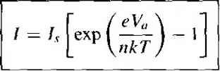 \A I JUNCTION BREAKDOWN the ideal pn junction, a reverse-bias voltage will result in a small reverse-bias current through the device. However, the reverse-bias voltage may not increase withoiit [limit; at some particular voltage, the reverse-bias current will increase rapidly. The )phed voltage at this point is called the breakdown voltage. Two physical mechanisms give rise to the reverse-bias breakdown in a pn junc-tion: the Zener effect and the avalanche effect. Zener breakdown occurs in highly )ped pn junctions through a tunneling mechanism. In a highly doped junction, the conduction and valence bands on opposite sides of the junction are sufficiently close during reverse bias that electrons may tunnel directly from the valence band on the p side into the conduction band on the n side. This tunneling process is schematically shown in Figure 8.22a. The avalanche breakdown process occurs when electrons and/or holes, moving across the space charge region, acquire sufficient energy from the electric field to create electron-hole pairs by colliding with atomic electrons within the depletion region. The avalanche process is schematically shown in Figure 8.22b. The newly created electrons and holes move in opposite directions due to the electric field and thereby add to the existing reverse-bias current. In addition, the newly generated electrons and/or holes may acquire sufficient energy to ionize other atoms, leading to the avalanche process. For most pn juncrions, the predominant breakdown mechanism will be the avalanche effect. If we assume that a reverse-bias electron current / o enters the depletion region at X - 0 as shown in Figure 8.23, the electron current will increase with distance through the depletion region due to the avalanche process. At л- - W, the electron p region n region 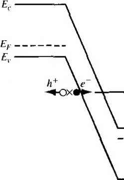 Diffusion ofeXcctroas  Space charge region { + ) E-field  - Pn Diffusion of holes Figure 8.22 f (a) Zener breakdown mechanism in a reverse-biased pn junction; (b) avalanche breakdown process in a reverse-biased pn junction. 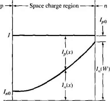 Figure 8.231 Electron and hole current components through the space charge region during avatanche multiplication. current may be written as (8,99) where M is a multiplication factor. The hole current is increasing through the depletion region from the n to p region and reaches a maximum value at jt 0. The, total current is constant through the pn junction in steady state. We can write an expression for the incremental electron current at some point .v as dlix) = InMan dx + Ip(x)ap dx (8.1(Ю) where a and ap are the electron and hole ionization rates, respectively. The ionization rates are the number of electron-hole pairs generated per unit length by an electron (a ) or by a hole (а^). Equation (8.100) may be written as dinix) (8.101) The total current / is given by I I,{x) + Ipix) (8 л 02) which is a constant. Solving for Ip{x) from Equation (8Л02) and substituting into Equation (8.101), we obtain dlnjx) dx -h (ap -a )f (x) =apl (8.103) If we make the assumption that the electron and hole ionization rates are equal so 8-4 J unction Breakdown then Equation (8.103) may be simplified and integrated through the space charge region. We will obtain / (W)~/ (0)-/ (8.105) Using Equation (8.99), Equation (8.105) may be written as МЛ.О-/ЛО) (8.106) Since M / n / and since / (0) ~ I , Equation (8.106) becomes (8.107) The avalanche breakdown voltage is defined to be the voltage at which M approaches infinity. The avalanche breakdown condition is then given by adx = 1 (8.108) The ionization rates are strong functions of electric field and, since the electric field is not constant through the space charge region. Equation (8.108) is not easy to evaluate. If we consider, for example, a one-sided p+n junction, the maximum electric field is given by eN,iX Ещах - (8.109) The depletion width .v is given approximately as (8.110) where Vr is the magnitude of the applied reverse-bias voltage. We have neglected the built-in potential V/ . If we now define Vr to be the breakdown voltage Vg, the maximum electric field, Eniax will be defined as a critical electric field, Eht. at breakdown. Combining Equations (8.109) and (8.110), wc may write (8.111) where Nr is the semiconductor doping in the low-doped region of the one-sided junction. The critical electric field, plotted in Figure 8.24, is a slight funcrion of doping. We have been considering a uniformly doped planar junction. The breakdown voltage will decrease for a linearly graded junction. Figure 8.25 shows a plot of the breakdown voltage for a one-sided abrupt junction and a linearly graded junction. If we take into account the curvature of a diffused junction as well, the breakdown voh-age will be further degraded. 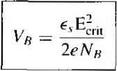 i 20 > 18 S. 16 с О о и [4 12 -Ю One-sided abiupt junction at 300 К 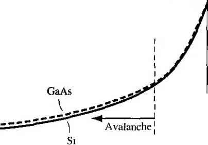 Tutneling 0 10 * i > i ] mil i I .....I -1 i J-LUU\ .......... 10 10 10 5xio Figure 8-241 Critical electric tield at breakdown in a onesided junction as a function of impurity doping concentrations. (FromSze {12].} Impurity concentratioTi Nf (cm ) IqL 1qJ6 д)17 1000 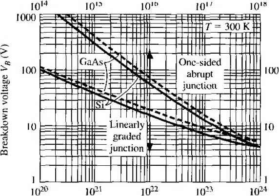 Impurity gradient a (cm Figure 8.25 J Breakdown voltage versus impurity concentration in uniformly doped and linearly graded junctions. (From Sze (121) DESIGN EXAMPLE 8.8  Objective To design an ideal one-sided n p junction diode to meet a breakdown voltage specification. Consider a silicon pn junction diode al Г = 300 К. Assume that jV,/ = 3 x 10 cm -*. Design the diode such that the breakdown voltage is = 100 V. Solution From Figure 8.25, we find that the doping concentration in the low-doped side of a one-sided abrupt junction should be approximately 4 x 10 cm for a breakdown voltage of 100 v.  8 - 5 Charge Storage and Diode Transients 309 For a doping concentration of 4 x 10cm~-\ the critical electric field, from Figure 8.24, is approximately 3.7 x lO* V/cm. Then from Equation (8.111), the breakdown voltage is 110 V, which correlates quite well with the results from Figure 8.25. Conclusion As Figure 8.25 shows, the breakdown voltage increases as the doping concentration decreases in the low-doped region. TEST YOUR UNDERSTANDING E8.13 A one-sided, planar, uniformly doped silicon pn junction diode is required to have a reverse-bias breakdown voltage of = 60 V. What is the maximum doping concentration in the low-doped region such that this specification is met? (t~3 tiOl X 8 Л^ * V) Е8Л4 Repeat E8.13 for a GaAs diode. (£-ШЭ ,01 x &T Af suy) *8.5 I CHARGE STORAGE AND DIODE TRANSIENTS The pn junction is typically used as an electrical switch. In forward bias, referred to as the on state, a relatively large current can be produced by a small applied voltage; in reverse bias, referred to as the offsiaie, only a very small current will exist. Of primary interest in circuit applications is the speed of the pn junction diode in switching states. We will qualitatively discuss the transients that occur and the charge storage effects. We will simply state the equations that describe the switching times without any mathematical derivations. 8.5.1 The T\irn-off Transient Suppose we want to switch a diode from the forward bias on state to the reverse-bias off state. Figure 8.26 shows a simple circuit that will switch the applied bias at r = 0. For r < 0, the forward-bias current is Ш 11f= (8.112) The minority carrier concentrations in the device, for the appHed forward voltage V/r, are shown in Figure 8.27a. There is excess minority carrier charge stored in both the p and n regions of the diode. The excess minority carrier concentrations at the space charge edges are supported by the forward-bias junction voltage V . When the voltage is switched from the forward- to the reverse-bias state, the excess minority carrier concentrations at the space charge edges can no longer be supported and they start to decrease, as shown in Figure 8.27b. The collapse of the minority carrier concentrarions at the edges of the space charge region leads to large concentration gradients and diffusion currents in the 1 ... 28 29 30 31 32 33 34 ... 55 |
|
© 2026 AutoElektrix.ru
Частичное копирование материалов разрешено при условии активной ссылки |