 |
 |
 |
| Главная Журналы Популярное Audi - почему их так назвали? Как появилась марка Bmw? Откуда появился Lexus? Достижения и устремления Mercedes-Benz Первые модели Chevrolet Электромобиль Nissan Leaf |
Главная » Журналы » Absorbing materialorganic polymer 1 ... 29 30 31 32 33 34 35 ... 55 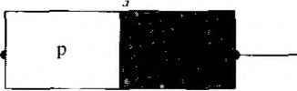 Figure 8.26 1 Simple circuit for switching a diode from forward to reverse bias. reverse-bias direction. If we assume, for the moment, that the vohage across diode junction is small compared with Vk, then the reverse-bias current is limited approximately (8.113] The junction capacitances do not allow the junction vohage to change instantaneously. If the current Ir were larger than this value, there would be a forward-bias voltage across the junction, which would violate our assumption of a reverse-bias current. If the current Ir were smaller than this value, there would be a reverse-bias voltage across the junction, which means that the junction voltage would have changed instantaneously. Since the reverse current is limited to the value given by Equation (8.113), the reverse-bias density gradient is constant; thus, the minority carrier concentrations at the space charge edge decrease with time as shown in Figure 8.27b. This reverse current Ir will be approximately constant for 0+ <t < , where is called the storage time. The storage time is the length of time required for the minority carrier concentrations at the space charge edge to reach the thermal-equilibrium values. After this time, the voltage across the junction will begin to change. The current characteristic is shown in Figure 8.28. The reverse current is the flow of the stored minority carrier charge, which is the difference between the minority carrier concentrations ait - 0~ and r - oo, as was shown in Figure 8.27b. The storage time t can be determined by solving the time-dependent continuity equarion. If we consider a one-sided p+n junction, the storage time is determined 8 ш 5 Charge Storage and Diode Transients Пр(х' =0) rtpQ exp Forward bias diffusion of eiectrons 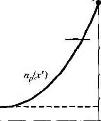 Forward bias diffusion of hoJes 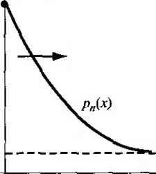 0 JC- 0 (a) 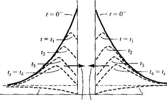 t Reverse bias \ diffusion electrons Reverse bias diffusion of holes Figure 8.27 1 (a) Steady-state forward-bias minority carrier concentrations; (b) minority carrier concentrations at various limes during switching. 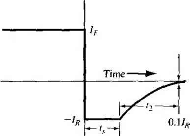 Figure 8.28 I Current characteristic versus time during diode switching. from the equation T/;o If h (8.1h where erf (л') is known as the error function. An approximate solution for the stoi time can be obtained as The recovery phase for / > is the time required for the junction to reach its steady-state reverse-bias condition. The remainder of the excess charge is hei removed and the space charge width is increasing to the reverse-bias value. 1.,. decay time Ь is determined from exp i-t2/Tpo) = 1+0.1 (8.116) The total turn-off time is the sum of and Гт- To switch the diode quickly, we need to be able to produce a large reverse cui-rent as well as have a small minority carrier lifetime. In the design of diode circuits, then, the designer must provide a path for the transient re verse-bias current pulse in order to be able to switch the diode quickly. These same effects will be considered when we discuss the switching of bipolar transistors. TEST YOUR UNDERSTAMDiNG Е8Л5 A one-sided pn silicon diode, that has a forward-bias current of . = 1.75 mA, is switched to reverse bias with an effective reverse-bias voltage of = 2 V and an effective series resistance of Rh =4 k. The minority carrier hole lifetime is 10~ s. (a) Determine the storage time f,. {b) Calculate the decay time . (c) What is the tum-off time of the diode? [s 01 X 3 (J) *s oi X gr I iq) *s . oi x 9170 0) suyl 8.5Д The Turn-on Transient The turn-on transient occurs when the diode is switched from its off*- state into the] forward-bias on state. The turn-on can be accomplished by applying a forward-bias current pulse. The first stage of turn-on occurs very quickly and is the length of rime required to narrow the space charge width from the reverse-bias value to its thermal-equilibrium value when Va = 0. During this time, ionized donors and ceptors are neutralized as the space charge width narrows. The second stage of the turn-on process is the time required to establish the minority-carrier distributions. During this time the voltage across the junction is increasing toward its steady-state value. A small turn-on time is achieved if the ininor- ity carrier lifetime is small and if the forward-bias current is small. 8 - 6 The Tunnel Diode 8.6 I THE TUNNEL DIODE The tunuel diode is a pn junction in which both the n and p regions are degenerately doped. As we discuss the operation of this device, we will find a region that exhibits a negative differential resistance. The tunnel diode was used in oscillator circuits in the past, but other types of solid-state devices are now used as high-frequency oscillators; thus, the tunnel diode is really only of academic interest. Nevertheless, this device does demonstrate the phenomenon of tunneling we discussed in Chapter 2. Recall the degenerately doped semiconductors we discussed in Chapter 4: the Fermi level is in the conduction band of a degenerately doped n-type material and in the valence band of a degenerately doped p-type material. Then, even at 7 = 0 K, electrons will exist in the conduction band of the n-type material, and holes (empty states) will exist in the p-type material. Figure 8.29 shows the energy-band diagram of a pn junction in thermal equilibrium for the case when both the n and p regions are degenerately doped. The deplefion region width decreases as the doping increases and may be on the order of approximately 100 A for the case shown in Figure 8.29. The potential barrier at the juncrion can be approximated by a triangular potenrial barrier, as is shown in Figure 8.30. This potential barrier is similar to the potential barrier used in Chapter 2 to illustrate the tunneling phenomenon. The barrier width is small and the electric field in the space charge region is quite large; thus, a finite probability exists that an electron may tunnel through the forbidden band from one side of the junction to the other. We may qualitatively determine the current-voltage characteristics of the tunnel diode by considering the simplified energy-band diagrams in Figure 8.31. n region p region  Space charge region Figure 8.291 Energy-band diagram of a pn junction in thermal equilibrium in which both the n and p regions are degenerately doped. Potential energy  Space charge region Figure 8.301 Triangular potential barrier approximation of the potential barrier in the tunnel diode.  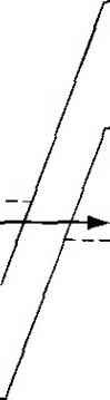 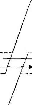 Figure 831 I Simplified energy-band diagrams and /-V characteristics of the tunnel diode at (a) zero bias; (b) a slight forward bias; (c) a forward bias producing maximum tunneling current. 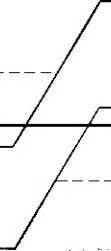  Figure 8.311 (concluded) (d) A higher forward bias showing less tunneling current; (e) a forward bias for which the diffusion current dominates. Figure 8.3la shows the energy-band diagram at zero bias, which produces zero current on the /-V diagram. If we assume, for simplicity, that we are near 0 K, then all energy states!are filled below Ef on both sides of the junction. Figure 8.3 lb shows the situation when a small forward-bias voltage is applied to the junction. Electrons in the conduction band of the n region are directly opposite to empty states in the valence band of the p region. There is a finite probability that some of these electrons will tunnel directly into the empty states, producing a forward-bias tunneling current as shown. With a slightly larger forward-bias voltage, as in Figure 8.31 c, the maximum number of electrons in the n region will be opposite the maximum number of empty states in the p region; this will produce a maximum tunneling current. As the forward-bias voltage continues to increase, the number of electrons on the n side direcdy opposite empty states on the p side decreases, as in Figure 8.3 Id, and the tunneling current will decrease. In Figure 8.31 e, there are no electrons on the  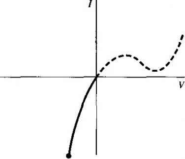 Figure 8.32 I (a) Simplified energy-band diagram of a tunnel diode with a reverse-bias voltage; (b) /-V characteristic of a tunnel diode with a reverse-bias voltage. n side directly opposite available empty states on the p side. For this forward-bif voltage, the tunneling current will be zero and the normal ideal diffusion current exist in the device as shown in the I-V characteristics. The portion of the curve showing a decrease in current with an increase in voltage is the region of differential negative resistance. The range of voltage and current: for this region is quite small; thus, any power generated from an oscillator using this j negative resistance property would also be fairly small. A simplified energy-band diagram of the tunnel diode with an applied reverse-bias voltage is shown in Figure 8.32a. Electrons in the valence band on the p side are directly opposite empty states in the conducrion band on the n side, so electrons can now tunnel directly from the p region into the n region, resulting in a large reverse-1 bias tunneling current. This tunneling current will exist for any reverse-bias voltage, i The reverse-bias current will increase monotonically and rapidly with reverse-bias voltage as shown in Figure 8.32b. 8.7 I SUMMARY When a forward-bias voltage is applied across a pn junction (p region positive with respect to the n region), the potential barrier is lowered so that holes from the p region and electrons from the n region can flow across the junction. The boundary conditions relating the minority carrier hole concentration in the n region at the space charge edge and the minority carrier electron concentrafion in the p region at the space charge edge were derived. The holes that are injected into the n region and the electrons that are injected into the p region now become excess minority carriers. The behavior of the excess minority carrier is described by the ambipolar transport equation developed and described in Chapter 6. Solving the ambipolar transport equation and using the boundary condifions, the steady-state minority carrier hole and electron concentrations in the n region and p region, respectively, were derived. р G lossary of I mportant Terms 317 Gradients exist in the minority carrier hole and electron concentrations so that minority carrier diffusion currents exist in the pn junction. These diffusion currents yield the ideal current-voltage relationship of the pn junction diode. The small-signal equivalent circuit of the pn junction diode was developed. The two parameters of interest are the diffusion resistance and the diffusion capacitance. Excess carriers are generated in the space charge region of a reverse-biased pn junction. These carriers are swept out by the electric field and create the reverse-bias generation current that is another component of the reverse-bias diode current. Excess carriers recombine in the space charge region of a forward-biased pn junction. This recombination process creates the forward-bias recombination current that is another component of the forward-bias diode current. Avalanche breakdown occurs when a sufficiently large reverse-bias voltage is applied to the pt\ junction. A large reverse-bias current may then be induced in the pn junction. The breakdown voltage as a function of the doping levels in the pn junction was derived. In a one-sided pn junction, the breakdown voltage is a function of the doping concentration in the low-doped region. When a pn junction is switched from forward bias to reverse bias, the stored excess minority carrier charge must be removed from the juncfion. The fime required to remove this charge is called the storage time and is a limiting factor in the switching speed of a diode. GLOSSARY OF IMPORTANT TERMS avalanche breakdown The process whereby a large reverse-bias pn juncfion current is created due to the generation of electron-hole pairs by the coLfision of electrons and/or holes with atomic electrons within the space charge region. carrier injection The flow of carriers across the space charge region of a pn junction when a voltage is applied. critical electric field The peak electric field in the space charge region at breakdown. diffusion capacitance The capacitance of a forward-biased pn juncfion due to minority carrier storage effects. diffusion conductance The ratio of a low-frequency, small-signal sinusoidal current to voltage in a forward-biased pn junction. diffusion resistance The inverse of diffusion conductance. forward bias The condition in which a positive voltage is applied to the p region with respect to the n region of a pn junction so that the potenfial barrier between the two regions is lowered below the thermal-equilibrium value. generation current The reverse-bias pn junction current produced by the thermal generation of electron-hole pairs within the space charge region. long diode A pn junction diode in which both the neutral p and n regions are long compared with the respecfive minority carrier diffusion lengths. recombination current The forward-bias pn junction current produced as a result of the flow of electrons and holes that recombine within the space charge region. reverse saturation current The ideal reverse-bias current in a pn junction. *shurt* diode A pn junction diode in which at least one of the neutral p or n regions is short compared to the respecfive minority carrier diffusion length. storage time The time required tor the excess minority carrier concentrations at the pi charge edge to go trom their steady-state values to zero when the diode is swiichec forward to reverse bias. CHECKPOINT After studying this chapter, the reader should have the ability to: Describe the mechanism of chaise flow across the space charge region of a pn junction when a forward-bias voltage is applied. State the boundary conditions for the minoriiy carrier concentrations at the edge of the . space charge region. Derive the expressions for the steady-state minority carrier concentrations in the pn junction, Derive the ideal current-voltage relationship for a pn junction diode. Describe the characteristics of a short diode. Describe what is meant by diffusion resistance and diffusion capacitance. Describe generation and recombination currents in a pn junction. Describe the avalanche breakdown mechanism in a pn junction. .3 Describe the turn-off transient response in a pn junction. REVIEW QUESTIONS 1. Why docs the potential barrier decrease in a forward-biased pn junction? 2. Write the boundary conditions for the excess tuinority carriers in a pn junction (a) under forward bias and (b) under reverse bias. 3. Sketch the steady-state minority carrier concentrations in a forward-biased pn junction. 4. Explain the procedure that is used in deriving the ideal current-voltage relationship iti a pn junction diode, 5. Sketch the electron and hole currents through a forward-biased pn junction diode. 6. What is meant by a short diode? 7. (a) Explain the physical mechanisin of diffusion capacitance, (b) What is diffusion resistance? 8. Explain the physical tncchanism of the (a) generation current and (b) recombination curretit. 9. Why does the breakdown voltage of a pn junction decrease as the doping concentration increases? 10. Explain what is meant by storage time. PROBLEMS Section 8.1 pn Junction Current 8Л ia) Consider an ideal pn junction diode at T - 300 К operating in the forward-bias region. Calculate the change in diode voltage that will cause a factor of 10 increase in current, (/?) Repeat part {a) for a factor of 100 increase in current. Problems 319
(a) Sketch the thermal equilibrium energy-band diagram of the pn junction, including the values of the Fermi level with respect to the intrinsic level on each side of the junction, (b) Calculate the reverse saturation current and determine the forward-bias current / at a forward-bias voltage of 0.5 V. (c) Determine the ratio of hole current to total current at the space charge edge x . 8.9 A germanium pn diode at Г = 300 К has the following parameters: /V = 10** cm iVj = 10 cm~-\ Dp - 49 cmVs, Д, - 100 cm/s, ro = ro = 5 ps, and A = \0~ cm. Determine the diode current for {a) a forward-bias voltage of 0.2 V and {b) a reverse-bias voltage of 0.2 V. 8Л0 An n+p silicon diode at Г = 300 К has the following parameters: Nj = 10 cm -*, Na - 10 cm~\ Dn = 25 cm/s. Dp = lOcm-/s, r () = Тро = 1 MS, and A = lO cm. Determine the diode current for (a) a forward-bias voltage of 0.5 V and (h) a reverse-bias voltage of 0.5 V.  Calculate the applied reverse-bias voltage at which the ideal reverse current in a pn junction diode at Г = 300 К reaches 90 percent of its reverse saturation current value. 8.3 An ideal sihcon pn junction at Г - 300 К is under forward bias. The minority carrier lifetimes are r o = 10~ s and ro = Ю s. The doping concentration in the n region L J J is At/ = 10 cm~-. Plot the ratio of hole current to the total current crossing the space charge region as the p-region doping concentration varies over the range 10- < Af, < 10 cm (Use a log scale for the doping concentrations.) 8.4 A silicon pn junction diode is to be designed to operate at T = 300 К such that the diode current is / = 10 mA at a diode voltage of Vi = 0,65 V. The ratio of electron current to total current is to be 0.10 and the maximum current density is to be no more i than 20 A/cm. Use the semiconductor parameters given in Example 8.2. fes For a silicon pn junction at T = 300 K, assume т^о = 0. lr o and д„ =2.4 Pp, The ratio of electron current crossing the depletion region to the total current is defined as the electron injection efficiency. Determine the expression for the electron injection efficiency as a function of (a) Nj/Ni and (b) the ratio of n-type conductivity to p-type conductivity. 8.6 Consider a p n silicon diode at 7 = 300 К with doping concentrations of A = 10 cm * and N = 10 cm -*. The minority carrier hole diffusion coefficient is Dp = \2cnr/s and the minority carrier hole lifetime is Т/,о = 10~ s. The cross-sectional area is A = 10 * cm-. Calculate the reverse saturation current and the diode current at a forward-bias voltage of 0.50 V. 8.7 Consider an ideal silicon pn junction diode with the following parameters: ro = ro = 0.1 x 10-Ч, D = 25 cm-/s. Dp = 10 cm/s. What must be the ratio of NJN so that 95 percent of the current in the deplefion region is carried by electrons? 8.8 A silicon pn junction with a cross-sectional area of I0~ cm has the following properties at T = 300 K: 1 ... 29 30 31 32 33 34 35 ... 55 |
|
© 2026 AutoElektrix.ru
Частичное копирование материалов разрешено при условии активной ссылки |