 |
 |
 |
| Главная Журналы Популярное Audi - почему их так назвали? Как появилась марка Bmw? Откуда появился Lexus? Достижения и устремления Mercedes-Benz Первые модели Chevrolet Электромобиль Nissan Leaf |
Главная » Журналы » Absorbing materialorganic polymer 1 ... 30 31 32 33 34 35 36 ... 55
XpX 0 X Figure 8.331 Figure for Problem 8.11. 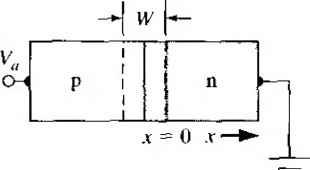 Figure 8.341 Figure for Problem 8.12. 8.11 A silicon step junction has uniform impurity doping concentrations of N = 5 x 8.12 8.13 8.14  8.15 8.16 8.17  10 cm-- and Л^ = 1 x 10 cm \ and a cross-sectional area of Л = 10 cm* Let Tnii = 0.4 fis and ipu = 0.1 д5. Consider the geometry in Figure 8.33. Calculate (a) the ideal reverse saturation current due to holes, ф) the ideal reverse saturation current due to electrons, (c) the hole concentration at x if 14 VJ -, and Ui) the electron current at x = jc -i- 3 L for V - Consider the ideal long silicon pn junction shown in Figure 834, T - 300 K. The n region is doped with 10* donor atoms per cm and the p region is doped with 5 X 10 acceptor atoms per cm\ The minority carrier lifetimes are т„ц = 0.05 s аш =0.01 fis. The minority carrier diffusion coefficients are D = 23 cm-/s and Df, = 8 cnr/s. The forward-bias voltage is = 0.610 V. Calculate (a) the excess hole concentration as a function of for x > 0, ф) the hole diffusion current density at.v = 3 x 10 cm, and (r) the electron current density at x = 3 x 10 cm. The limit of low injection is normally defined to be when the minority carrier concentration at the edge of the space charge region in the low-doped region becomes equal to one-tenth the majority carrier concentration in this region. Determine the value of the forward-bias voltage at which the limit of low injection is reached for the diode described in (я) Problem 8.9 and ф) Problein 8.10. The cross-sectional area of a sihcon pn junction is 10 cm. The temperature of the diode is 7 = 300 K, and the doping concentrations are = lO* cm * and N = 8 x 10 cm . Assume minority carrier lifetimes of т„[, = 10 s and tq - 10~ s. Calculate the total number of excess electrons In the p region and the total number of excess holes in the n region for (a) V ~ 0.3 V, Ф) V = OA V, and {c) V 0.5 V. Consider two ideal pn junctions at Г = 300 К, having exactly the same electrical and physical parameters except for the bandgap energy of the semiconductor materials. The first pn junction has a bandgap energy of 0.525 eV and a forward-bias current of 10 mA with V = 0.255 V. For the second pn junction, design the bandgap energy so that a forward-bias voltage of V = 0.32 V will produce a current of 10 дА. The reverse-bias saturation current is a function of temperature, {a) Assuming that /j varies with temperature only from the intrinsic carrier concentration, show that we can write /, CT exp (-E/kT) where С is a constant and a function only of the diode parameters, ф) Determit\e the increase in Л as the temperature increases from T = 300 к to 7 = 400 К for a (0 germanium diode and ( ) silicon diode. Assume that the mobilities, diffusion coefficients, and minority carrier lifefime parameters are independent of temperature (use the T = 300 К values). Assume that t = 10- s, ro = 10 s, М/ 5 x 10 cnr\ and /V 5 x 10** cm-\ Plot the ideal reverse saturation current density from T 200 К to 7 = 500 К for (a) silicon, [{b) germanium, and (c) gallium arsenide ideal pn junctions. (Use a log scale for the current density.) 8 An ideal uniformly doped silicon pn junction diode has a cross-sectional area of 10 * cm. The p region is doped with 5 x 10 acceptor atoms per cm * and the n region is doped with 10 donor atoms per cm. Assume that the following parameter values are independent of temperature: = 1.10 eV, t q = т^,[) - 10~ s, = 25 cm-/s, D, = lOcm/s, Л^, = 2.8 x 10 cm-\and Л^ = 1.04 x 10* cm \ The ratio of the forward to reverse current is to be no less than 10 with forward- and reverse-bias voltages of 0,50 V. Also, the reverse saturation current is to be no larger than 1 дА. What is the maxitnuin temperature at which the diode will meet these specifications? *8.I9 A p n silicon diode is fabricated with a narrow n region as shown in Figure 8.10, in which W < L. Assume the boundary condition of p, = /7 o at .r jt -h W . (a) Derive the expression for the excess hole concentrafion Sp (x) as given by Equation (8.27). (i ) Using the results of part (o), show that the current density in the diode is given by Problems 321 8.20 A silicon diode can be used to measure temperature by operating the diode at a fixed forward-bias current. The forward-bias voltage is then a function of temperature. At T = 300 K, the diode voltage is found to be 0.60 V. Determine the diode voltage at (a) T = 310 К and [h] T 320 K. 8.21 A forward-biased silicon diode is to be used as a temperature sensor The diode is forward biased with a constant current source and K, is measured as a function of temperature, (a) Derive an expression for V {T) assuming that D/L for electrons and holes, and are independent of temperature, (b) If the diode is biased at = 0.1 mA and if Д = 10-A at T = 300 K, plot versus Tfor 20С <: Г < 200X. (с) Repeat part (h) if It) = 1 mA. (J) Determine any changes in the results of parts (a) through (c) if the change in bandgap energy with temperature is taken into account. Section 8.2 Small-Signal Model of the pn Junction 8*22 Calculate the small-signal ac admittance of a pn junction biased at K, = 0.72 V and Ioq =2.0 mA. Assume the minority carrier lifetime is 1 д5 in both the n and p regions. T = 300 K. 8.23 Consider a p+ n silicon diode at Г = 300 К, The diode is forward biased at a current of 1 mA. The hole lifetime in the n region is 10 s. Neglecting the depletion capacitance, calculate the diode impedance at frequencies of 10 kHz, 100 kHz, I MHz, and 10 MHz. 8.24 Consider a silicon pn junction with parameters as described in Problem 8.8. {a) Calculate and plot the depletion capacitance and diffusion capacitance over the voltage range -10 < S 0.75 V. (t) Determine the voltage at which the two capacitances are equal 8.25 Consider a p n silicon diode at T = 300 K. The slope of the diffusion capacitance versus forward-bias current is 2.5 x 10 F/A. Determine the hole lifetime and the diffusion capacitance at a forward-bias current of 1 mA. 8.26 A one-sided n p silicon diode at Г 300 К with a cross-sectional area of 10 cm is operated under forward bias. The doping levels are = 10 cm and  Na - 10 cm~-, and the minority carrier parameters are ro = 10 ro = 10 s, = 10 cm-/s, and D = 25 cm-/s. The maximum diffusion capacitance is to be 1 Determine (a) the maximum current through the diode, (/?) the maximum forward-bi voltage, and (c) the diffusion resistance. 8.27 A silicon pn juncdon diode at 7 = 300 К has a cross-sectional area of 10 - cm , length of the p region is 0.2 cm and the length of the n region is 0.1 cm. The doping concentrations are Nj = 10 cm~ and Na = 10 cm~ Determine (й) approximately the series resistance of the diode and (b) the current through the diode that produce a 0.1 V drop across this series resistance. 8.28 We want to consider the effect of a series resistance on the forward bias voltage required to achieve a particular diode current, (o) Assume the reverse saturation current in a diode is Д = 10 A at 7 = 300 K. The resistivity of the n region is 0.2 -cm and the resistivity of the p region is 0,1 Q-cm, Assume the length of each neutral region is 10 - cm and the cross-sectional area is 2 x 10~ cm. Determine the required applied voltage to achieve a current of (0 1 mA and 00 Ю mA. {h) Repeat par\ (u> neglecting the series resistance. 8.29 The minimum small-signal diffusion resistance of an ideal forward-biased silicon pn junction diode at Г 300 К is to be = 48 The reverse saturation current is Л = 2 X 10~ A. Calculate the maximum applied forward-bias voltage that can be applied to meet this specification. 8.30 (a) An ideal silicon pn junction diode at 7 = 300 К is forward biased at Va = -f-20 mV. The reverse-saturation current is = 10 * A. Calculate the small-signal diffusion resistance, (b) Repeat part (a) for an applied reverse-bias voltage of K, = -20 mV, Section 8.3 Generation-Recombination Currents 8.31 Consider a reverse-biased gallium arsenide pn junction at Г = 300 К. Assume that a reverse-bias voltage, Vr = 5 V, is applied. Assume parameter values of; Na = Aj =: 10 civr\ Dp = 6 cm/s, D = 200 cm/s, and ro = r o = Го = 10 s. Calculate the ideal reverse saturation current density and the reverse-biased generation current density. How does the relative value of these two currents compare to those of the silicon pn junction? *8.32 (a) Consider Example 8,7. Assume that all parameters except n, are independent of temperature. Determine the temperature at which 7, and У^п will be equal. What are the values of and У^п at this temperature? {b) Using the results of Example 8.7, calculate the forward-bias voltage at which the ideal diffusion current is equal to the recombination current. 8.33 Consider a GaAs pn diode at T = 300 К with Na - Nj ~ \f) cm~ and with a cross-sectional area of 10 * cm. The minority carrier mobilities are д„ - 3000 cmVV-s and \ip = 200cmЛ/-s.The lifetimes are ro - r o - 4= 10 s. As a first approxitna-tion, assume the electron-hole generation and recombination rates are constant across the space charge region, {a) Calculate the total diode current at a reverse-bias voltage of 5 V and at forward-bias voltages of 0.3 V and 0.5 V. {b) Compare the results of part {a) to an ideal diode at the same applied voltages. 8.34 Consider the pn junction diode described in Problem 8.33. Plot the diode recombination current and the ideal diode current (on a log scale) versus forward bias voltage over the range 0.1 < V,; < l.OV. Problems Tllumi nation 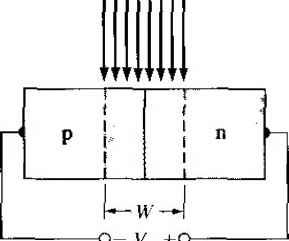 Figure 8.35 I Figure for Problem 8.38 and 8.39. 8.35 A silicon pn junction diode at T = 300 К has the following parameters:УУ = N,t = 10 cm-\ = r o = To = 5 X 10 s, - 10 cnr/s, Д, = 25 cmVs, and a cross-sectional area of lO * cm-. Plot the diode recombination current and the ideal diode current (on a log scale) versus forward bias voltage over the range 0. J < V, < 0.6 V. 8.36 Consider a GaAs pn diode at Г = 300 К with N 10 cm and with a cnjss-sectional area of 5 x 10~- cm-. The minority carrier mobilities are д„ 3500 cm- A-s and Pp = 220 cm-/V-s. The electron-hole lifetimes are т^о - r() = Го = 10~ s. Plot the diode forward-bias current including recombination current between diode voltages of 0J < V/;, < 1.0 V. Compare this plot to that for an ideal diode. *8.37 Starting with Equation (8.83) and using the suitable approximations, show that the maximum recombination rate in a forward-biased pn junction is given by Equation (8.91). 8.38 Consider, as shown in Figure 8.35, a uniformly doped silicon pn junction at T = 300 К with impurity doping concentrations of Л^ = TVj = 5 x 10 cm~ and minority carrier lifetimes of т„о = ro = fо = 10~ s. A reverse-bias voltage of Vr - 10 V is applied. A light source is incident only on the space charge region, producing an excess carrier generation rate of = 4 x 10 cm~ s . Calculate the generation current density. 8.39 Along silicon pn junction diode has the following parameters: Nj = 10 cm~-, = 3 X 10 cm \ r f) = Г;Н) = = 10 s, 18 cm-/s, and Of, = 6 cmVs. A light source is incident on the space charge region such as shown in Figure 8.35, producing a generation current density of Jc = 25 mA/cm-. The diode is open circuited. The generation current density forward biases the junction, inducing a forward-bias current in the opposite direction to the generation current. A steady-state condition is reached when the generation current density and forward-bias current density are equal in magnitude. What is the induced forward-bias voltage at this steady-state condition? Section 8.4 Junction Breakdown 8.4U The critical electric field for breakdown in silicon is approximately E rit - 4 X 10 v/cm. Determine the maximum n-type doping concentration in an abrupt p n junction such that the breakdown voltage is 30 V.  8.41 Design an abrupt sihcon p n junction diode that has a reverse breakdown voltage 120 V and has a forward-bias current of 2 mA at V = 0.65 V. Assume that т^ = 10~ s, and find fi, from Figure 5.3. 8.42 Consider an abrupt np GaAs junction with a p-type doping concentration of = 10 cm *. Determine the breakdown voltage. 8.43 A symmetrically doped silicon pn junction has doping concentrations of = Nj = 5 X 10 cm~. If the peak electric field in the junction at breakdown is E = 4 x 10 V/cm, determine the breakdown voltage of this junction, 8.44 An abrupt silicon p n junction has an n-region doping concentration of N,i 5 X 10- cm~. What must be the minimum n-region width such that avalanche brei down occurs before the depletion region reaches an ohmic contact (punchthrough)? 8.45 A silicon pn junction diode is doped with = Nj = 10* cm . Zener breakdown occurs when the peak electric field reaches 10 V/cm. Determine the reverse-bias breakdown voltage. 8.46 A diode will very often have the doping profile shown in Figure 7.19, which is known as an n pp diode. Under reverse bias, the depletion region must remain within the p region to avoid premature breakdown. Assume the p region doping is Ю^ cm~. Determine the reverse-bias voltage such that the depletion region remains within the p region and does not reach breakdown if the p region width is {a) 15 fim and (h) 150 дт. For each case, state whether the maximum depletion width or the breakdown voltage is reached first. 8.47 Consider a silicon pn junction at Г - 300 К whose doping profile varies linearly from = 10 cm to iV = Ю' cm -* over a distance of 2 /xm. Estimate the breakdown voltage. Section 8.5 Charge Storage and Diode Transients 8.48 (a) In switching a pn junction froiu forward to reverse bias, assume that the ratio of reverse current, До forward current, /f, is 0.2. Determine the ratio of storage time to minority carrier lifetime, tJipQ. (h) Repeat part (a) if the ratio of ? to is 1.0. 8.49 A pn junction is switched from forward to reverse bias. We want to specify that = 0.2г;,о. Determine the required ratio of Ir to . to achieve this requirement. In this case, determine f2/t,o. 8.50 Consider a diode with a junction capacitance of 18 pF at zero bias and 4.2 pF at a reverse bias voltage of = 10 V. The minority carrier lifetimes are 10~ s. The diode is switched from a forward bias with a current of 2 mA to a reverse bias voltage of 10 V applied through a 10 kQ resistor Estimate the tum-off time. Section 8.7 The Tunnel Diode 8.51 Consider a silicon pn junction at Г = 300 К with doping concentration of Nj = Na = 5 X 10* cm~-. Assuming the abrupt junction approximation is valid, determine the space charge width at a forward-bias voltage of - 0.40 V. 8.52 Sketch the energy-band diagram of an abrupt pn junction under zero bias in which the p region is degenerately doped and Ec = Ef in the n region. Sketch the forward- and reverse-bias current-voltage characteristics. This diode is sometimes called a hack-ward diode. Why? Reading List Summary and Review 8.53 (a) Explain physically why the diffusion capacitance is not important in a reverse-biased pn junction, (b) Consider a silicon, a germanium, and gallium arsenide pn junction. If the total current density is the same in each diode under forward bias, discuss the expected relative values of electron and hole current densities. *8.54 A silicon pn junction diode at Г = 300 К is to be designed to have a reverse-bias breakdown voltage of at least 50 V and to handle a forward-bias current of lo ~ 100 m A while still operating under low injecdon. The minority carrier diffusion coefficients and lifefimes are = 25 cm/s, Z>, = 10 cm/s, and Zno = Трц = 5 x \0~ s. The diode is to be designed for minimum cross-sectional area. *8.55 The donor and acceptor concentrarions on either side of a silicon step junction are equal, (a) Derive an expression for the breakdown voltage in terms of the critical electric field and doping concentration, (b) If the breakdown voltage is to be Vg = 50 V, specify the range of allowed doping concentrations. READING LIST E Dimitrijev, S. Understanding Semiconductor Devices. New York: Oxford University Press, 2000. 2. Kano, K. Semiconductor Devices. Upper Saddle River, NJ: Prentice Hall, 1998. 3. Muller, R. S., and T. I. Kamins. Device Electronics for Integrated Circuits. 2nd ed. New York: Wiley, 1986. 4. Neudeck, G. W. The PN Junction Diode, Vol. 2 of the Modular Series on Solid State Devices. 2nd ed. Reading, MA: Addison-Wesley, 1989. *5. Ng, K. K. Complete Guide to Semiconductor Devices. New York: McGraw-Hill, 1995. 6. Pierret, R. E Semiconductor Device Fundamentals. Reading, MA; Addison-Wesley Publishing Co., 1996. 7. Roulston, D. J. A Introduction to the Physics of Semiconductor Devices, New York: Oxford University Press, 1999. 8. Shur, M. Introduction to Electronic Devices. New York: John Wiley and Sons, Inc., 1996. *9. Shur, M. Physics of Semiconductor Devices. Englewood Cliffs, NJ: Prentice Hall, 1990. 10. Streetman, B. G., and S. Banerjee. Solid State Electronic Devices. 5th ed. Upper Saddle River, NJ: Prentice Hall, 2000. 11. Sze, S. M. Physics of Semiconductor Devices. 2nd ed. New York: John Wiley & Sons, 1981. 12. Sze, S. M. Semiconductor Devices: Physics and Technology. 2nd ed. New York: John Wiley and Sons, 2001. *13. Wang, S. Fundamentals of Semiconductor Theory and Device Physics. Englewood Cliffs, NJ: Prentice Hall, 1989. 14. Yang, E. S- Microelectronic Devices, New York: McGraw-Hill, 1988.  Е R  Metal-Semiconductor and Semiconductor Heterojunctions PREVIEW In the preceding two chapters, we considered the pn junction and assumed that the semiconductor material was the same throughout the entire structure. This type of junction is referred to as a homojunction. We developed the electrostatics of the junction and derived the current-voltage relationship. In this chapter, we will consider the metal-semiconductor junction and the semiconductor heterojunction, in which the material on each side of the junction is not the same. These junctions can also produce diodes. Semiconductor devices, or integrated circuits, must make contact with the outside world. This contact is made through nonrectifying metal-semiconductor junctions, or ohmic contacts. An ohmic contact is a low-resistance junction providing current conducrion in both directions. We will examine the conditions that yield metal-semiconductor ohmic contacts. 9.1 1 THE SCHOTTKY BARRIER DIODE One of the first practical semiconductor devices used in the early 1900s was the metal-semiconductor diode. This diode, also called a point contact diode у was made by touching a metallic whisker to an exposed semiconductor surface. These metal-semiconductor diodes were not easily reproduced or mechanically reliable and were replaced by the pn junction in the 1950s. However, semiconductor and vacuum technology is now used to fabricate reproducible and reliable metal-semiconductor contacts. In this section, we will consider the metal-semiconductor rectifying contact, or Schottky barrier diode. In most cases, the rectifying contacts are made on n-type semiconductors; for this reason we will concentrate on this type of diode. 9ЛЛ Qualitative Characteristics The ideal energy-band diagram for a particular metal and n-type semiconductor before making contact is shown in Figure 9.1 a. The vacuum level is used as a reference level. The parameter 0,;, is the metal work function (measured in volts), is the semiconductor work function, and x i known as the electron affinity. The work functions of various metals are given in Table 9.1 and the electron affinities of several semiconductors are given in Table 9.2. In Figure 9.1a, we have assumed that Фт > Фб- The ideal thermal-equilibrium metal-semiconductor energy-band diagram, for this situation, is shown in Figure 9.1b. Before contact, the Fermi level in the semiconductor was above that in the metal. In order for the Fermi level to become a constant through the system in thermal equilibrium, electrons from the semiconductor flow into the lower energy states in the metal. Positively charged donor atoms remain in the semiconductor, creating a space charge region. The parameter фв is the ideal barrier height of the semiconductor contact, the potential barrier seen by electrons in the metal trying to move into the semiconductor. Vacuum level 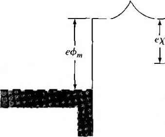  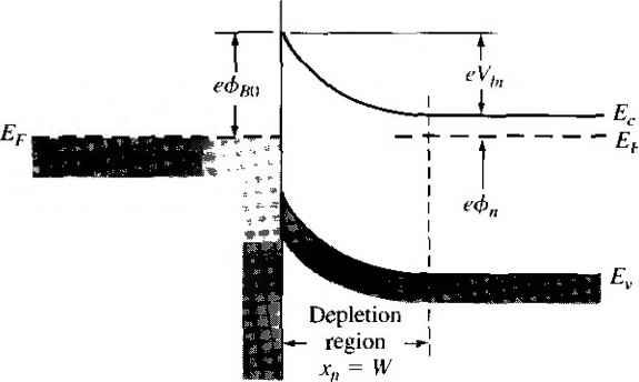 Figure 9Л I (a) Energy-band diagram of a metal and semiconductor before contact; (b) ideal energy-band diagram of a metal-n-semiconductor junction for ф„, > .
Table 9.21 Electron affinity of some semiconductors
This bairier is known as the Schottky barrier and is given, ideally, by ФВО = (Фт - X) On the sen\iconductor side, V is the built-in potential barrier. This barrier, similar to the case of the pn junction, is the barrier seen by electrons in the conduction band trying to move into the metal. The built-in potential barrier is given by Уы -~ ФбО - Фп (9.2) which makes Уы a slight function of the semiconductor doping, as was the case in a pn junction. If we apply a positive voltage to the semiconductor with respect to the metal, the semiconductor-to-metal barrier height increases, while ф^о remains constant in this idealized case. This bias condition is the reverse bias. If a positive voltage is applied to the metal with respect to the semiconductor, the semiconductor-to-inetal barrier Vi is reduced while again remains essentially constant. In this situation, electrons can more easily flow from the semiconductor into the metal since the barrier has been reduced. This bias condition is the forward bias. The energy-band diagrams for the reverse and forward bias are shown in Figures 9.2a and 9.2b, where Vr is the magnitude of the reverse-bias voltage and V is the magnitude of the forward-bias voltage. The energy-band diagrams versus voltage for the metal-sem icond uctor junction shown in Figure 9.2 are very similar to those of the pn junction given in the last chapter. Because of the similarity, we expect the current-voltage characteristics of the Schottky barrier junction to be similar to the exponential behavior of the pn junction diode. The current mechanism here, however, is due to the flow of majority carrier electrons. In forward bias, the barrier seen by the electrons in the semiconductor is reduced, so majority carrier electrons flow more easily from the semiconductor into the metal. The forward-bias current is in the direction from metal to semiconductor; it is an exponential function of the forward-bias voltage Kj. 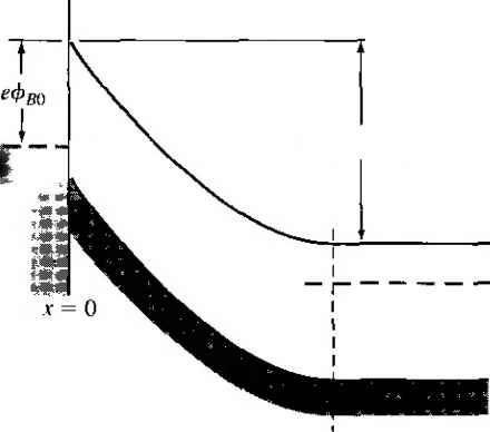 X = X
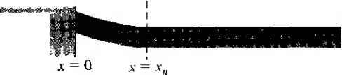 Figure 9.2 1 Ideal energy-band diagram of a mctal-sem iconductor junction (a) under reverse bias and (b) under forftard bias. 9Л<2 Ideal Junction Properties We can determine the electrostatic properties of the junction in the same way as we FM for the pn junction. The electric field in the space charge region is determined mPoissons equation. We have that dE p(x) (9.3) where p(x) is the space charge volume density and 6 is the permittivity of the semiconductor. If we assume that the semiconductor doping is uniform, dien by integrat- - dx ---h C (9.4) where Ci is a constant of integration. The electric field is zero at the space charge edge in the semiconductor, so the constant t)f integration can be found as eN,iXn C, =: (9-5) The electric field can then be written as E ----(л- -x) (9.6) which is a hnear funcrion of distance, for the uniformly doped semiconductor, and reaches a peak value at the metal-sem iconductor interface. Since the E-field is zero inside the metal, a negative surface charge must exist in the metal at the metal-semiconductor j uncti on. 1 ... 30 31 32 33 34 35 36 ... 55 |
||||||||||||||||||||||||||||||||||||||||||||||||||
|
© 2026 AutoElektrix.ru
Частичное копирование материалов разрешено при условии активной ссылки |