 |
 |
 |
| Главная Журналы Популярное Audi - почему их так назвали? Как появилась марка Bmw? Откуда появился Lexus? Достижения и устремления Mercedes-Benz Первые модели Chevrolet Электромобиль Nissan Leaf |
Главная » Журналы » Absorbing materialorganic polymer 1 ... 31 32 33 34 35 36 37 ... 55 The space charge region width, W, may be calculated as we did for the pn junction. The result is identical to that of a one-sided p n junction. For the uniformly doped semiconductor, we have (9.7) where Vr is the magnitude of the applied reverse-bias voltage. We are again assuming an abrupt junction approximation. 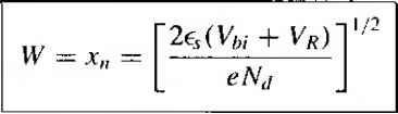 EXAMPLE 9.1 Objective To calculate the theoretical barrier height, buill-in potential barrier, and maximum electlic field in a metal-semiconductor diode for zero applied bias. Consider a contact between tungsten and n-type silicon doped to Nj - 10 cm at T = 300 K. Solution The metal work function for tungsten (W) from Table 9.1 is <> , = 4.55 V and the elect affinity for silicon from Table 9.2 is x =4.01 V. The barrier height is then Фви = Фш -X= 4.55 - 4.01 = 0.54 V where is the ideal Schottky barrier height. We can calculate ф„ as ф„ = - In 0.0259 In 2.8 x 10 206 V Then Уы = Фно - Фп = 0.54 - 0.206 = 0.33 V The space charge width at zero bias is ni/2 2(ll.7)(8.85 x 10--*)(0.33) (1.6 x 10⁻⁹)(10) jc = 0.207 x 10- cm Then the maximum electric field is eNjXn (1.6 x 10-)( 10)(0.207 x lO ) так (ll.7)(8.85 x 10-) or finally mJi = 3.2 x 10* V/cm Comment The values of space charge width and electric field are very similar to those obtained for a pn junction. A junction capacitance can also be detenninQd in the same way as we did for the pn junction. We have that С - eN г (9.8) where С is the capacitance per unit area. If we square the reciprocal of Equation (9.8), we obtain 2{Vbi + Vr) (9.9) We can use Equation (9.9) to obtain, to a first approximation, the built-in potential barrier V/ , and the slope of the curve from Equation (9.9) to yield the semiconductor doping N,i. We can calculate the potential 0 , and then determine the Schottky barrier фво from Equation (9.2). TEST YOUR UNDERSTANDING Е9Л Consider an ideal chromium-lo-n-type silicon Schottky diode at T = 300 K. Assume the semiconductor is doped at a concentration of N,i = Ъ x cm~. Determine the (a) ideal Schottky barrier height, (b) buih-in potential barrier, (c) peak electric field with an applied reverse-bias voltage ofV = 5 V, and {d) juncfion capacitance per unit area for Vj? = 5 V, 6-01 x 889 = D (P) /A fO\> L= P) Л еего = A (Q) Ч 6i7o = Ф w *suvl E9.2 Repeat E9.1 for an ideal palladium-to-n-type GaAs Schouky diode with the same impurity concentration, [шад oi x gg-q = 3 (p) ип/д qi x i = (j) A 616*0 = (Ф Ч eO*l = <?(f?) -suvl Objective To calculate the semiconductor doping and Schottky barrier height from the silicon diode experimental data shown in Figure 9.3. T = 300 K. Solution The intercept of the tungsten-silicon curve is approximately at Уы = 0.40 V. From Equa-. tion (9.9), we can write d(l/C) A(l/C) EXAMPLE 9.2 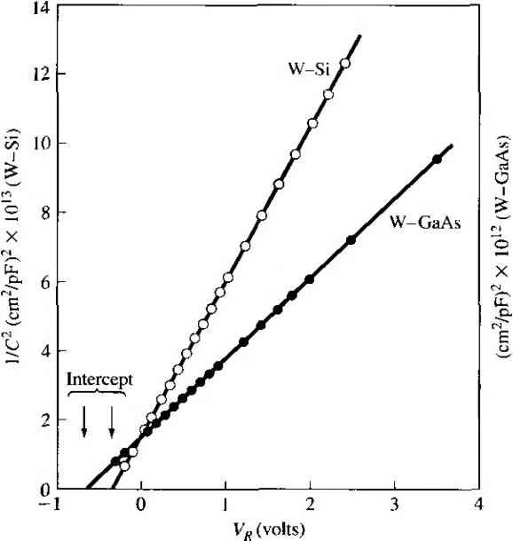 Figure 9.3 I versus for W-Si and W-GaAs Schottky barrier diodes. (FromSze [14}.) Then, from the figure, we have so that 17 -3 (1.6 x 10-i)(lL7)(8.85 x 10-*)(4.4 x \0) 2.7 X 10 cm We can calculate kT Фп = - In (N,\ /2.8x10 so that Фвп = Уы +Фп= ОАО + 0Л2 = 0.52 V where фвп is the actual Schottky barrier height. Comment The experimental value of 0.52 V can be compared with the ideal barrier height of = 0.54 V found in Example 9.1. These results agree fairly well. For other metals, the discrepancy between experiment and theory is larger. We can see that the built-in potential barrier of the gallium arsenide Schottky diode is larger than that of the silicon diode. This experimental result is normally observed for all types of metal contacts. M.3 Nonideal Effects on the Barrier Height Several effects will alter the actual Schottky barrier height from the theoretical value given by Equation (9.1). The first effect we will consider is the Schottky effect, or , image-force-induced lowering of the potential barrier. I An electron in a dielectric at a distance x from the metal will create an electric rfield. The field lines must be perpendicular to the metal surface and will be the same as if an image charge, -\-e, is located at the same distance from the metal surface, but inside the metal. This image effect is shown in Figure 9.4a. The force on the electron, due to the coulomb attraction with the image charge, is = -E (9Л0) Metal +---- 1 - Шш. Dielectric E{x) x = G (a)  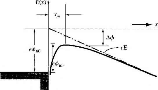 x = 0 Figure 9.4 1 (a) Image charge and electric field lines at a metal-dielectric interface, (b) Distortion of the potenfial barrier due to image forces with zero electric field and (c) with a constant electric field. The potential can then be found as ф(х) = + Г Edx - + f --- - dx - - У \6kCsX (9Л1) where x is the integration variable and where we have assumed that the potential is zero at jr = oo. The potential energy of the electron is -еф(х); Figure 9.4b is a plot of the potential energy assuming that no other electric helds exist. With an electric field present in the dielectric, the potential is modified and can be written as щ -0(л-)---Ev (9.12) 1 DJTCvX The potential energy of the electron, including the effect of a constant electric field, is plotted in Figure 9.4c. The peak potential barrier is now lowered. This lowering of the potential barrier is the Schottky effect, or image-force-induced lowering. We can ftnd the Schottky barrier lowering, A<, and the position of the maximum barrier, x, , from the condition that d(eф(x)) dx (9.13) We find that 16jr6vE (9.14) 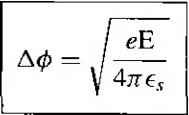 (9Л5) EXAMPLE 9.3 Objective To calculate the Schottky barrier lowering and the position of the maximum barrier height. Consider a gallium arsenide metal-semiconductor contact in which the electric field in the semiconductor is assumed to be E = 6.8 x V/cm. Solution The Schottky barrier lowering is given by Equation (9.15), which in this case yields E 4jre, (1.6 x 10-)(6.8 x 10) 4jr(13.I)(8.85 x lO-*) = 0.0273 V The position of the maximum barrier height is (1.6 X 10-) 167г6,Е V I6jr(l3.0(8.85 x 10 i)(6.8 x W) jr =2 X 10- cm:-20A Comment Although the Schottky barrier towering may seem like a small value, the barrier height and the barrier towering will appear in exponential terms in the current-voltage relationship. A small change in the barrier height can thus have a significant effect on the current in a Schouky barrier diode. TEST YOUR UNDERSTANDING E9.3 Determine the Schottky barrier lowering and the position of the maximum barrier height for the junction described in E9T. Use the value of the electric field found in this exercise, (y t = A €6Z0*0 = 0V E9.4 Repeat E9.3 for the junction described in E9.2. (V 8 61 = A ШОО = suy) Figure 9.5 shows the measured barrier heights in gallium arsenide and silicon Schottky diodes as a function of metal work functions. There is a monotonic relation between the measured barrier height and the metal work function, but the curves do not fit the simple relarion given in Equation (9.1). The barrier height of the > 1.0 - 0.8 - 0.2 -
4.0 5.0 Metal work function, еф (eV) Figure 9.5 1 Experimental barrier heights as a function of metal work functions for GaAs and Si. (From Crowley and Sze [2}.)  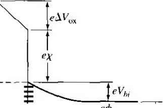 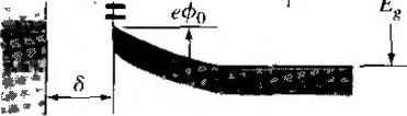 Figure 9.6 I Energy-band diagram of a metal-semiconductor junction with an interfacial layer and interface states. metal-semiconductor junction is determined by both the metal work function and semiconductor surface or interface states. A more detailed energy-band diagram of a metal to n-type semiconductor cont in thermal equilibrium is shown in Figure 9.6. We will assume that a narrow interfa layer of insulator exists between the metal and semiconductor. The interfacial layer i support a potential difference, but will be transparent to the flow of electrons betwe< the metal and semiconductor. The semiconductor also shows a distriburion of surf a states at the metal-semiconductor interface. We will assume that all states below surface potential фо are donor states, which will be neutral if the state contains an ek Iron and positively charged if the state does not contain an electron. We will also sume that all states above фо are acceptor states, which will be neutral if the state d( not contain an electron and negatively charged if the state contains an electron. The diagram in Figure 9.6 shows some acceptor states above фо and below Ер\ These states will tend to contain electrons and will be negatively charged. We assume that the surface state density is constant and equal to Djj states/cm-eV. relation between the surface potential, surface state density, and other sem icon duct( parameters is found to be I /-------- €( (9.16) We will consider two limiting cases. Case 1 Let Dit oc. In this case, the right side of Equation (9.16) goes to zero. We then have Ф fit} (9.1 The barrier height is now fixed by the bandgap energy and the potential фо- The barrier height is totally independent of the metal work function and the semiconductor electron affinity. The Fermi level becomes pinned at the surface, at the surface potential фо- Case 2 Let DjfS 0. Equation (9.16) reduces to Фви - (Фт - X) which is the original ideal expression. The Schottky barrier height is a function of the electric field in the semiconductor through the barrier lowering effect. The barrier height is also a function of the sur-face states in the semiconductor. The barrier height, then, is modified from the ideal theoretical value. Since the surface state density is not predictable with any degree of certainty, the barrier height must be an experimentally determined parameter. 9.1.4 Current-Voltage Relationship The current transpoil in a metaJ-semiconductor junction is due mainly to majority carriers as opposed to minority carriers in a pn junction. The basic process in the recrifying contact with an n-type semiconductor is by transport of electrons over the potential barrier, which can be described by the thermionic emission theory. The thermionic emission characteristics arc derived by using the assumptions that the barrier height is much larger than kT, so that the Maxwell-Boltzmann approximation applies and that thermal equilibrium is not affected by this process. Figure 9.7 shows the one-diinensional barrier with an applied forward-bias voltage Va and shows two electron current density components. The current Jsm is the electron current density due to the flow of electrons from the semiconductor into the metal, and the current J is is the electron current density due to the flow of electrons from the metal into the seiniconductor. The subscripts of the currents indicate the direction of electron flow. The conventional current direction is opposite to electron flow. The current density Л , is a function of the concentrarion of electrons which have ji-directed velocities sufficient to overcome the barrier. We may write dn (9.18) where E is the minimum energy required for thermionic emission into the metal, Vj, is the carrier velocity in the direction of transport, and e is the magnitude of the electronic charge. The incremental electron concentrarion is given by dn=gAE)ff(E)dE (9.19) where gc(E) is the density of states in the conduction band and fr(E) is the Fermi-Dirac probability function. Assuming that the Maxwell-Boltzmann approximation applies, we may write 4я(2т*)/ dn -- sIe - Ec exp -JE-Ef) kT dE (9.20) 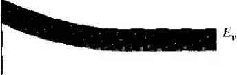 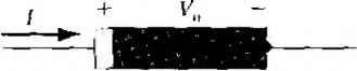 + Va - Figure 9,7 I Energy-band diagram of a forward-biased metal-semiconductor junction including the image lowering effect- If all of the electron energy above Ec is assumed to be kineric energy, then wehai (9.21 The net current density in the metal-to-semiconductor junction can be written as which is defined to be positive in the direction from the metal to the semiconductor. We find that 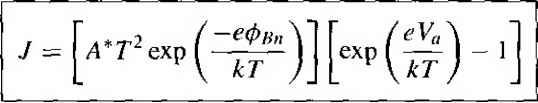 (9.23) where 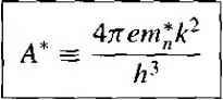 The parameter A* is called the effective Richardson constant for thermionic emission. Equation (9.23) can be written in the usual diode form as (9.25) 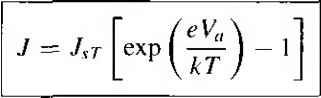 where Л? is the reverse-saturation current density and is given by 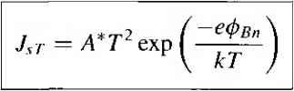 (9.26) We may recall that the Schottky barrier height changes because of the image-force lowering. We have that фвп - Фно A0. Then we can write Equation (9.26) as T л*2 ( -Фво\ (е1\ф Jj - AT exp [ -\ exp (927) The change in barrier height, Аф, will increase with an increase in the electric field, or with an increase in the applied reverse-bias voltage. Figure 9.8 shows a typical reverse-bias current-voltage characteristic of a Schottky barrier diode. The reverse-bias current increases with reverse-bias voltage because of the barrier lowering effect. This figure also shows the Schottky barrier diode going into breakdown. 10- - i 10-* k Expcrimentili result  Theoretical result 10 10 10 Vr (volts) Figure 9.81 Experimental and theoretical reverse-bias currents in a PtSi-Si diode. (From Sze [Ml) 1 ... 31 32 33 34 35 36 37 ... 55 |
|
© 2026 AutoElektrix.ru
Частичное копирование материалов разрешено при условии активной ссылки |