 |
 |
 |
| Главная Журналы Популярное Audi - почему их так назвали? Как появилась марка Bmw? Откуда появился Lexus? Достижения и устремления Mercedes-Benz Первые модели Chevrolet Электромобиль Nissan Leaf |
Главная » Журналы » Absorbing materialorganic polymer 1 ... 32 33 34 35 36 37 38 ... 55 EXAMPLE 9.4 Objective To calculate the effective Richardson constant from the /-V characteristics. Consider the tungsten-silicon diode curve in Figure 9.9 and assume a barrier height of =0.67 V. From the figure, Jr 6 x 10 A/cm . Solution We have that kT ) so that JsT (еф A = - exp -ефвЛ кТ ) Then 6 x 10 (300) / 0.67 \ Comment The experimentally determined value of Л * is a very strong function of фи since фц is in exponential term. A small change in фвп will change the value of the Richardson const substantially. 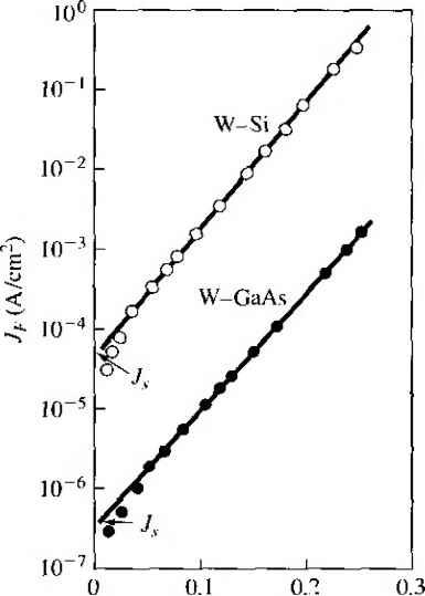 0Л 0.2 V, (volt) Figure 9.9 1 Forward-bias current density Jf versus V,j for Wi-Si and W-GaAs diodes. (From Sze I Ml) TEST YOUR UNDERSTANDING E9.5 The Schottky barrier height of a silicon Schottky junction \фв 0.59 V, the effective Richardson constant is A* = 114 A/K-cm-, and the cross-sectional area is Л = 10~ cm. For T = 300 K, calculate (a) the ideal reverse-saturation current and (b) the diode current for V 0.30 V. Iv VPl = f (Я) У -01 ]£] = 7 ( ) -suy] We may note that the reverse-saturation current densities of the tungsten-siHcon and tungsten-gallium arsenide diodes in Figure 9.9 differ by approximately 2 orders of magnitude. This 2 order of magnitude difference will be reflected in the effective Richardson constant, asmming the barrier heights in the two diodes are essentially the same. The definition of the effective Richardson constant, given by Equation (9.24), contains the electron effective mass, which differs substantially between sihcon and gallium arsenide. The fact that the effective mass is in the expression for the Richardson constant is a direct result of using the effective density of states function in the thermionic emission theory. The net result is that A* and Л7 will vary widely between silicon and gallium arsenide. 9.1.5 Comparison of the Schottliy Barrier Diode and the pn Junction Diode Although the ideal current-voltage relationship of the Schottky barrier diode given by Equation (9.25) is of the same form as that of the pn junction diode, there are two important differences between a Schottky diode and a pn juncrion diode: The first is in the magnitudes of the reverse-saturation current densities, and the second is in the switching characterisrics. The reverse-saturation current density of the Schottky barrier diode was given by Equarion (9.26) and is J,T = A*Texp The ideal reverse-saturation current density of the pn junction diode can be written as eDpp Efi Lp (9.28) The form of the two equations is vastly different, and the current mechanism in the two devices is different. The current in a pn junction is determined by the diffusion of minority carriers while the current in a Schottky barrier diode is determined by thermionic emission of majority carriers over a potential barrier. Objective To calculate the reverse-saturation current densities of a Schottky barrier diode and a pn junction diode. Consider a tungsten barrier on silicon with a measured barrier height of =0.67 eV. The effective Richardson constant is = 114 A/K-cm Let T = 300 K. EXAMPLE 9.5 Solution If we neglect the barrier lowering effect, we have for the Schottky barrier diode Л 7 = Л*Г^ехр -еф1 kT (114)(300) exp f 7- - 5.98 x 10 - A/cm 0.0259 Consider a silicon pn junction with the following parameters at 7 = 300 K. Na = 10 cm-- Nj 10 cm- Dp = lOcmVs г/! (} 25 cnr/s 10- s We can then calculate the following parameters. Lp = \,Ox 10- cm Pno = 2.25 x 10 cm L = 1.58 x 10-- cm Пр = 2.25 X 10 cm- The ideal revcrse-saiuration current density of the pn junction diode can be determined fro Equation (9.28) as Щ J (1.6 x 10-)(25)(2.25 x 10) (1.6 x 10 )(10)(2.25 x 10 ) (1.58x10--) ~ (l.bxlO-) 5.7 x 10- + 3.6 x 10- = 3.66 x 10 A/cm Comment The ideal reverse-saturation current density of the Schottky barrier junction is orders of magnitude larger than that of the ideal pn junction diode. < 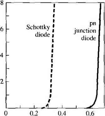 Vjy (volts) Figure 9.10 I Comparison of forward-bias characteristics between a Schottky diode and a pn junction diode. Recall that the reverse-bias current in a silicon pn junction diode is dominated by the generation current. A typical generation current density is approximately 10 A/cm, which is still 2 to 3 orders of magnitude less than the reverse-saturation current density of the Schottky barrier diode. A generation current also exists in the reverse-biased Schottky barrier diode; however, the generation current is negHgible compared with the Л7 value. Since Jj > , the forward-bias characterisrics of the two types of diodes will also be different. Figure 9.10 shows typical l-V characteristics of a Schottky barrier j diode and a pn junction diode. The effective turn-on voltage of the Schottky diode is less than that of the pn junction diode. Objective example 9.6 l To calculate the forward-bias voltage required to generate a forward-bias current density of 10 A/cm- in a Schottky barrier diode and a pn junction diode. Consider diodes with the parameters given in Example 9.5. We can assume that the pn junc-i tion diode will be sufficiently forward biased so that the ideal diffusion current will dominate. Let Г = 300 K. Solution For the Schottky barrier diode, we have Neglecting the (-1) term, we can solve for the forward-bias voltage. We find Уа = = УгУп(-\ = (0.0259) In (----Л =0.312 V For the pn juncfion diode, we have V = V,l (() = (0.0259) in () = 0.682 V ш Comment A comparison of the two forward-bias voltages shows that the Schottky barrier diode has a I tim)-on voltage that, in this case, is approximately 0.37 V smaller than the tum-on voltage of the pn junction diode. The actual difference between the turn-on voltages will be a funcrion of the barrier height of the metal-semiconductor contact and the doping concentrations in the pn junction, but the relatively large difference will always be realized. We will consider one application that urilizes the difference in turn-on voltage in the next chapter, in what is referred to as a Schottky clamped transistor. TEST YOUR UNDERSTANDING E9.6 (a) The reverse saturation currents of a pn junction and a Schottky diode are 10 A and 10 A, respectively. Determine Ihe required forward-bias voltages in the pn junction diode and Schottky diode to produce a current of 100 A in each diode. {h) Repeat pan {a) for forward bias currents of 1 mA, [A ЯЯ£0 A 990 Л Ш'О Л 96C0 Н Е9.7 А рп junction diode and а Schouky diode have equal cross-sectional areas and havej forward-biased currents of 0.5 mA. The reverse-saturation current of the Schottky diode is 5 x 10 A. The difference in forward-bias vohage between the two diodes is 0.30 V. Determine the reverse-saturation current of the pn junction diode. (V j-OI X The second major difference between a Schottky barrier diode and a pn juncti( diode is in the frequency response, or switching characteristics. In our discussion, have considered the cunent in a Schottky diode as being due to the injection of maj< ity earners over a potential barrier. The energy-band diagram of Figure 9.1, for exi pie, showed that there can be electrons in the metal directly adjacent to empty states the semiconductor. If an electron froin the valence band of the semiconductor were flow into the metal, this effect would be equivalent to holes being injected into semiconductor. This injection of holes would create excess minority carrier holes the n region. However, calculations as well as measurements have shown that the rati< of the minority carrier hole current to the total current is extremely low in most c< The Schottky barrier diode, then, is a majority carrier device. This fact mt that there is no diffusion capacitance associated with a forward-biased Schott diode. The elimination of the diffusion capacitance makes the Schottky diode higher-frequency device than the pn junction diode. Also, when switching a Schol diode from forward to reverse bias, there is no minority carrier stored charge remove, as was the case in the pn junction diode. Since there is no minority canrit storage time, the Schottky diodes can be used in fast-switching applications. A typical switching rime for a Schottky diode is in the picosecond range, while for pn junction it is normally in the nanosecond range. 9.2 I METAL-SEMICONDUCTOR OHMIC CONTACTS Contacts must be made between any semiconductor device, or integrated circuit, and the outside world. These contacts are made via ohmic contacts. Ohmic contacts are metal-to-semicouductor contacts, but in this case they are not rectifying contacts. An ohmic contact is a low-resistance junction providing conduction in both directions between the metal and the semiconductor. Ideally, the current through the ohmic contact is a linear function of applied voltage, and the applied voltage should be very small. Two general types of ohmic contacts are possible: The first type is the ideal nonrectifying barrier, and the second is the tunneling barrier. We will define a specific contact resistance that is used to characterize ohmic contacts. 9 - 2 Metal-Semicond uctor Ohm ic Contacts 9.2.1 Ideal Nonrectifying Barriers We considered an ideal metal-to-n-type semiconductor contact in Figure 9.1 for the case when 0 > 0,. Figure 9.11 shows the same ideal contact for the opposite case of ф, < фs. In Figure 9.11a we see the energy levels before contact and, in Figure 9.1 lb, the barrier after contact for thermal equilibrium. To achieve thermal equilibrium in this junction, electrons will flow from the metal into the lower energy states in the semiconductor, which makes the surface of the semiconductor more n type. The excess electron charge in the n-type semiconductor exists essentially as a surface charge density. If a positive voltage is applied to the metal, there is no barrier to electrons flowing from the semiconductor into the metal. If a positive voltage is applied to the semiconductor, the effective barrier height for electrons flowing from the metal into the semiconductor will be approximately фвп - фп which is fairly small for a moderately to heavily doped semiconductor. For this bias condition, electrons can easily flow from the metal into the semiconductor. Figure 9.12a shows the energy-band diagram when a positive voltage is applied to the metal with respect to the semiconductor. Electrons can easily flow downhill from the semiconductor into the metal. Figure 9.12b shows the case when a positive voltage is applied to the semiconductor with respect to the metal. Electrons can easily flow over the barrier from the metal into the semiconductor. This junction, then, is an ohinic contact Figure 9T3 shows an ideal nonrectifying contact between a metal and a p-type semiconductor. Figure 9.13a shows the energy levels before contact for the case when ф„ > When contact is made, electrons from the semiconductor will flow into the metal to achieve thermal equilibrium, leaving behind more empty states, or holes. The excess concentration of holes at the surface makes the surface of the semiconductor more p type. Electrons from the luetal can readily move into the empty states in the semiconductor. This charge movement corresponds to holes flowing ефл  Figure 9.111 Ideal energy-band diagram (a) before contact and (b) after contact for a metal-n-semiconductor junction for < фs. 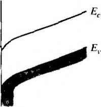 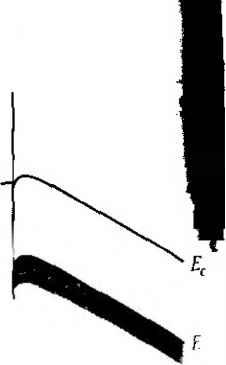 Figure 9.12 I Ideal energy-band diagram of a metal-n-semiconductor ohmic contact (a) wit a positive voltage applied to the metal and (b) with a positive voltage applied to the semiconductor 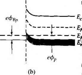 Figure 9.13 I Ideal energy-band diagram (a) before contact and (b) after contact for a metal-p-semiconductor junction for<; > 0,. from the semiconductor into the metah We can also visualize holes in the metal flowing into the semiconductor This junction is also an ohmic contact. The ideal energy bands shown in Figures 9.11 and 9Л 3 do not take into account the effect of surface states. If we assume that acceptor surface states exist in the upper half of the semiconductor bandgap, then, since all the acceptor states are below Et for the case shown in Figure 9.11b, these surface states will be negatively charged, and will alter the energy-band diagram. Similarly, if we assume that donor surface states exist in the lower half of the bandgap, then all of the donor states will be positively charged for the case shown in Figure 9,13b; the positively charged surface states will also alter this energy-band diagram. Therefore, if ф, < ф^ for the metal-n-type semiconductor contact, and if ф^ > Фs for the metal-p-type semiconductor contact, we may not necessarily form a good ohmic contact. 9,2.2 Tunneling Barrier The space charge w idth in a rectifying metal-semiconductor contact is inversely proportional to the square root of the semiconductor doping. The width of the depletion 9.2 Metal-Semiconductor OInmic Contacts 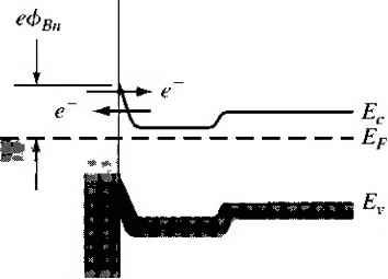 Figure 9.14 I Energy-band diagram of a heavily doped n-semiconductor-to-metal junction. gion decreases as the doping concentration in the semiconductor increases; thus, as the doping concentration increases, the probability of tunneling through the barrier in-creases. Figure 9.14 shows a junction in which the metal is in contact with a heavily idoped n-type epitaxial layer. Objective b calculate the space charge width for a Schottky barrier on a heavily doped semiconductor. Consider silicon at Г = 300 К doped at M = 7 x 10* cm -\ Assume a Shottky barrier with фвп = 0.67 V. For this case, we can assume that V) фщ. Neglect the barrier lowering effect. Solution From Equation (9.7), we have for zero applied bias 26, V -.1/2 2(11.7)(8.85 X 10-)(0.67) (1.6 X 10-l)(7 X lOiS) nl/2 EXAMPLE 9.7 1.1 X 10- cm = 110 A Comment In a heavily doped semiconductor, the depletion width is on the order of angstroms, so that tunneling is now a distinct possibility. For these types of barrier widths, tunneling may become the dominant current mechanism. The tunneling current has the form Jr ОС exp where (9.29) eh Na OO 2 V 6,m* The tunneling current increases exponentially with doping concentration. 9.2.3 Specific Contact Resistance A figure of merit of ohmic contacts is the specific contact resistance, 7?. This pi eter is defined as the reciprocal of the derivative of current density with respect voltage evaluated at zero bias. We may write Q-cnr (9,311 *=() We want R: to be as small as possible for an ohmic contact. For a rectifying contact with a low to moderate semiconductor doping concei tration, the current-voltage relation was given by Equation (9.23) as Л = A*T exp The thermionic emission current is dominant in this junction. The specific cont resistance for this case is then (9.32J The specific contact resistance decreases rapidly as the barrier height decreases. For a metal-semiconductor junction with a high impurity doping concentrati( the tunneling process will dominate. From Equations (9.29) and (9.30), the specifi( contact resistance is found to be Rc oc exp +2д/т* фип (9.33) which shows that the specific contact resistance is a very strong function of semiconductor doping. Figure 9.15 shows a plot of the theoretical values of Rc as a function of semiconductor doping. For doping concentrations greater than approximately 10 cm the tunneling process dominates and Rc shows the exponential dependence on Л^. For lower doping concentrations, the Rc values are dependent on the barrier heights and become almost independent of the doping. Also shown in the figure are experimental data for platinum silicide-silicon and aluminum-silicon junctions. Equation (9.33) is the specific contact resistance of the tunneling junction, which corresponds to the metal-to-n* contact shown in Figure 9Л4. However, the n n junction also has a specific contact resistance, since there is a barrier associated with this junction. For a fairly low doped n region, this contact resistance may actually dominate the total resistance of the junction. The theory of forming ohmic contacts is straightforward. To form a good ohmic contact, we need to create a low barrier and use a highly doped semiconductor at the surface. However, the actual technology of fabricating good, reliable ohmic contacts is not as easy in practice as in theory. It is also more difficult to fabricate good ohmic 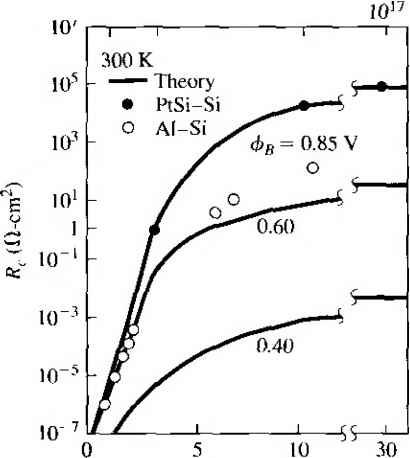 Figure 9.15 I Theoretical and experimental specific contact resistance as a function of doping. (From Sze [14].) contacts on wide-bandgap materials. In general, low barriers are not possible on these materials, so a heavily doped semiconductor at the surface must be used to form a tunneling contact. The formation of a tunneling junction requires diffusion, ion implantation, or perhaps epitaxial growth. The surface doping concentration in the semiconductor may be limited to the impurity solubility, which is approxi- mately 5 X 10 cm~ for n-type GaAs. Nonuniformities in the surface doping concentration may also prevent the theorerical limit of the specific contact resistance from being reached. In practice, a good deal of empirical processing is usually required before a good ohmic contact is obtained. 9.3 I HETEROJUNCTIONS In the discussion of pn junctions in the previous chapters, we assumed that the semiconductor material was homogeneous throughout the entire structure. This type of juncrion is called a homojunction. When two different semiconductor materials are used to form a junction, the junction is called a semiconductor heterojunction. As with many topics in this text, our goal is to provide the basic concepts concerning the heterojuncrion. The complete analysis of heterojunction structures involves quantum mechanics and detailed calcularions that are beyond the scope of this text. The discussion of heterojunctions will, then, be limited to the introduction of some basic concepts. 1 ... 32 33 34 35 36 37 38 ... 55 |
|
© 2026 AutoElektrix.ru
Частичное копирование материалов разрешено при условии активной ссылки |