 |
 |
 |
| Главная Журналы Популярное Audi - почему их так назвали? Как появилась марка Bmw? Откуда появился Lexus? Достижения и устремления Mercedes-Benz Первые модели Chevrolet Электромобиль Nissan Leaf |
Главная » Журналы » Absorbing materialorganic polymer 1 ... 33 34 35 36 37 38 39 ... 55 Е £.1 /,2 - E,2 vl (a) (b) (c) Figure 9.16 I Relation between narrow-bandgap and wide-bandgap energies: (a) straddling, (b) staggered, and (c) broken gap. 93Л Heterojunction Materials Since the two materials used to form a heterojunction will have different e bandgaps, the energy band will have a discontinuity at the junction interface. We have an abrupt junction in which the semiconductor changes abruptly from a n bandgap material to a wide-bandgap material. On the other hand, if we have GaAs-AlvGaj As system, for example, the value of лс may continuously vary o\\ distance of several nanometers to form a graded heterojunction. Changing the \a of .V in the AlvGai vAs system allows us to engineer, or design, the bandgap energy. In order to have a useful heterojunction, the lattice constants of the two materials must be well matched. The lattice match is important because any lattice mismakh can introduce dislocations resulting in interface states. For example, germanium anil galhum arsenide have lattice constants matched to within approximately 0.13 percent. Germanium-gallium arsenide heterojunctions have been studied quite extensively. More recently, gallium arsenide-aluminum gallium arsenide (GaAs-AlGaAs) junctions have been investigated quite thoroughly, since the lattice constants of GaAs and the AlGaAs system vary by no more than 0.14 percent. 9.3.2 Energy-Band Diagrams In the formation of a heterojunction with a narrow-bandgap material and a wide-bandgap material, the alignment of the bandgap energies is important in determininii the characteristics of the junction. Figure 9.16 shows three possible situations. In ure 9.16a we see the case when the forbidden bandgap of the wide-gap material completely overlaps the bandgap of the narrow-gap material. This case, called strad-dling, applies to most heterojunctions. We will consider only this case here. The other possibilities are called staggered and broken gap and are shown in Figures 9.16b and 9.16c. There are four basic types of heterojunction. Those in which the dopant type changes at the junction are called anhotype. We can forn\ nP or Np junctions, where the capital letter indicates the larger-bandgap material. Heterojunctions with the sar dopant type on either side of the junction are called isotype. We can form nN and isotype heterojunctions. Figure 9.17 shows the energy-band diagrams of isolated n-type and P-type materials, with the vacuum level used as a reference. The electron affinity of the Vacuum level 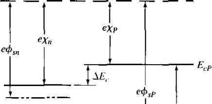 GaAs Figure 9,17 I Energy-band diagrams of a narrow-bandgap and a wide-bandgap material before contact. wide-bandgap material is less than that of the narrow-bandgap material. The difference between the two conduction band energies is denoted by А£:, and the difference between the two valence band energies is denoted by AE. From Figure 9Л7, we can see that AEc = eixn - Xp) AEc-\- A£i, = Ep - = A£ (934a) (9.34b) In the ideal abrupt heterojunction using nondegenerately doped semiconductors, the vacuum level is parallel to both conduction bands and valence bands. If the vacuum level is conrinuous, then the same and Af, disconrinuiries will exist at the heterojunction interface. This ideal situation is known as the electron affinity rule. There is still some uncertainty about the applicability of this rule, but it provides a good starting point for the discussion of heterojunctions. Figure 9.18 shows a general ideal nP heterojuncrion in thermal equilibrium. In order for the Fermi levels in the two materials to become aligned, electrons from the narrow-gap n region and holes from the wide-gap P region must flow across the junc-[ tion. As in the case of a homojunction, this flow of charge creates a space charge region in the vicinity of the metallurgical juncrion. The space charge width into the n-type region is denoted by jc and the space charge width into the P-type region is denoted by j. The discontinuities in the conduction and valence bands and the change in the vacuum level are shown in the figure. 9.3.3 Two-Dlmensional Electron Gas Before we consider the electrostatics of the heterojunction, we will discuss a unique characteristic of an isotype junction. Figure 9.19 shows the energy-band diagram of an nN GaAs-AlGaAs heterojunction in thermal equilibrium. The AlGaAs can be moderately to heavily doped n type, while the GaAs can be more lightly doped or
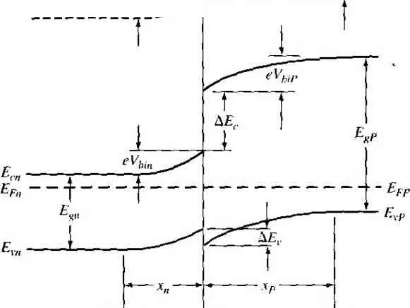 X -X, .v = 0 Figure 9Л81 Ideal energy-band diagram of an nP heterojunction in thennaJ equilibrium. 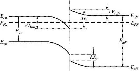 Figure *>.19i Ideal energy-band diagram of an nN heterojunction in thermal equilibrium. even intrinsic. As nentioned previously, to achieve thermal equilibrium, elect from the wide-bandgap AlGaAs flow into the GaAs, forming an accuinulation lay< of electrons in the potential well adjacent to the interface. One basic quantum-1 mechanical result that we have found previously is that the energy of an electron contained in a potential well is quantized. The phrase two-dimensional electron gas refers to the condition in which the electrons have quantized energy levels in one spatial direction (perpendicular to the interface), but are free to move in the other two spatial directions. The potential function near the interface can be approximated by a triangular potential well. Figure 9.20a shows the conduction band edges near the abrupt junction Viz) к  GaAs AlGaAs 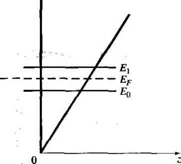 Figure 9.20 I (a) Conduction-band edge at N-AlGaAs, n-GaAs heterojunction; (b) triangular well approximation with discrete electron energies. 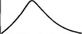 Figure 9.21 I Electron density in triangular potential well. interface and Figure 9.20b shows the approximation of the triangular potential well. We can write Vix) = eBz z>0 z<0 (9.35a) (9.35b) Schrodingers wave equation can be solved using this potential function. The quantized energy levels are shown in Figure 9.20b. Higher energy levels are usually not considered. The qualitative distribution of electrons in the potenrial well is shown in Figure 9.21. A current parallel to the interface will be a function of this electron concentrarion and of the electron mobility. Since the GaAs can be hghtly doped or intrinsic, the two-dimensional electron gas is in a region of low impurity doping so that impurity scattering effects are minimized. The electron mobility will be much larger than if the electrons were in the same region as the ionized donors. 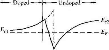 AlGaAs GaAs Figure 9.22 I Conduction-band edge at a graded heterojunction. The movement of the electrons parallel to the interface will still be influenced the coulomb attraction of the ionized impurities in the AlGaAs. The effect of thf forces can be further reduced by using a graded AlGaAs-GaAs heterojunction. The graded layer is AlGaiv As in which the mole fraction x varies with distance. In this case, an intrinsic layer of graded AlGaAs can be sandwiched between the N-type AlGaAs and the intrinsic GaAs. Figure 9.22 shows the conduction-band edges across a graded AlGaAs-GaAs heterojunction in thermal equilibrium. The electrons in the potential well are further separated from the ionized impurities so that the electron mobility is increased above that in an abrupt heterojunction. *9.3-4 Equilfbrium Electrostatics We will now consider the electrostatics of the nP heterojunction that was shown in Figure 9.18. As in the case of the homojunction, potential differences exist across the space charge regions in both the n region and the P region. These potential differences correspond to the built-in potential barriers on either side of the junction. The built-in potential barrier for this ideal case is defined as shown in Figure 9.18 to be the potential difference across the vacuum level. The built-in potential barrier is the sum of the potential differences across each of the space charge regions. The heterojunction built-in potential barrier, however, is not equal to the difference between the conduction bands across the junction or the difference between the valence bands across the junction, as we defined for the homojunction. Ideally, the total built-in potential barrier Уы ean be found as the difference between the work functions, or (936) Equation (9.36), from Figure 9.17, can be written as Vbi = lxp + EgP - {Efp- E p)\ - [eXn + E - {Е^ь - £vn)] (9.37a) eiXf - Xn) + (Ep - E,n) + (£r - E, ) - (Efp - E,p) (9.37b) which can be expressed as f fiV. - - AF. -\- AF. IT in (- eVbi = + A£, +Пп( - -kT\n(-] (9.38) V Pno / \PpoJ Finally, we can write Equation (9.38) as еУы^АЕ,.+кТ\и(\ (9.39) where ppo and pf , are the hole concentrations in the P and n materials, respectively, and yv,. and N,p are the effective density of states functions in the n and P materials, respectively. We could also obtain an expression for the built-in potential barrier in tenms of the conduction band shift as еУы - -Д+ кТ In f ) (9.40) Objective example 9.8 To determine AF,.. Ai\ , and for an n-Ge to P-GaAs heterojunction using the electron affinity rule. Consider n-type Ge doped with = 10 cm * and P-type GaAs doped with = 10* cm-\ Let T = 300 К so that , = 2.4 x 10 cm for Ge. Solution From Equation (9.34a), we have AE, eixn -Xp) = e(4.U - 4.07) = 0.06 eV and from Equation (9.34b), we have AE, = AE - Д£, = (1.43 - 0.67) - 0.06 = 0.70 eV To determine Уы using Equation (9.39), we need (o determine pno in Ge, or nr (2.4x10 )- , , Then {10)(6 X 10) еУы = 0.70-h (0.0259) In or, finally. (5.76 X 100)(7 X 10*) Уы l.OV Comment There is a nonsymmetry in the A £, and AE- values that will tend to make the potential barriers seen by electrons and holes different. This nonsymmetry does not occur in homoj unctions. We can deternaine the electric field and potential in the junction from Poissonii equation in exactly the same way as we did for the homojunction. For homogeneoi doping on each side of the junction, we have in the n region {-x < X < 0) (9.41 and in the P region ------{Xp -x) (0 < jc < Xp) (9.41b where € and ep are the permittivities of the n and P materials, respectively. We note that E - 0 at я = -л„ and Bp 0 at x - xp. The electric flux density D continuous across the junction, so which gives б„Е^(л = 0) = €pEp{x = 0) dfiXn KipXp (9.42i (9.421 Equation (9.42b) simply states that the net negative charge in the P region is equal to] the net positive charge in the n region-the same condition we had in a pn homo-; junction. We are neglecting any interface states that may exist at the heterojunction.; The electric potential can be found by integrating the electric field through the] space charge region so that the potential difference across each region can then be de-] termined. We find that eNdnxi (9.43a), (9,43b) Equation (9.42b) can be rewritten as (9.44) The ratio of the built-in potential barriers can then be determined as У bin P Ndn xl epNaP (9.45), Assuming that and c are of the same order of magnitude, the larger potential difference is across the lower-doped region. The total built-in potential barrier is If we solve for jc, for example, from Equation (9.42b) and substitute into Equa-don (9.46), we can solve for x as pNapVbi Kin+cpNap) (9.47a) We can also find Xp = (9.47b) The total depletion width is found to be 2€nCp(N,N,pfVbi W = Xy,-{- xp (948) If a reverse-bias voltage is applied across the heterojunction, the same equations apply if Vi is replaced by + V/?. Similarly, if a forward bias is applied, the same equations also apply if Vi is replaced by Уы - As before, У^ is the magnitude of the reverse-bias voltage and is the magnitude of the forward-bias voltage. As in the case of a homoj unction, a change in depletion width with a change in juncfion voltage yields a junction capacitance. We can find for the nP junction (F/cm) (9-49) eNj Nape ep A plot of (1 /CjY versus Ун again yields a straight line. The extrapolation of this plot of (1/Cj) = 0 is used to find the built-in potential barrier, V . Figure 9.18 showed the ideal energy-band diagram for the nP abrupt heterojunction. The experimentally determined values of AE and A£t, may differ from the ideal values determined using the electron affinity rule. One possible explanation for this difference is that most heterojunctions have interface states. If we assume that the electrostatic potential is continuous through the junction, then the electric flux density will be discontinuous at the heterojunction due to the surface charge trapped in the interface states. The interface states will then change the energy-band diagram of the semiconductor heterojunction just as they changed the energy-band diagram of the metal-semiconductor junction. Another possible explanation for the deviation fi:om the ideal is that as the two materials are brought together to form the heterojunction, the electron orbitals of each material begin to interact with each other, resulting in a transition region of a few angstroms at the interface. The energy bandgap is then continuous through this transition region and not a characteristic of either material. However, we still have the relation that Д£,: + A£, = A£ (9-50) for the straddling type of heterojuncrion, although the A and Д values may differ from those determined from the electron affinity rule. We may consider the general characteristics of the energy-band diagrams of the other types of heterojuncrion. Figure 9,23 shows the energy-band diagram of an Np 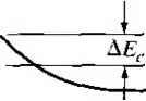 Figure 9.23 i Ideal energy-band diagram of an Np heterojunction in thennal equilibrium. 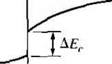 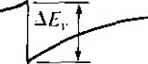 Figure 9.24 I Ideal energy-band diagram of a pP heterojunction in thermal equilibrium. heterojunction. The same AEc and A£r discontinuities exist, although the general shape of the conduction band, for exainple, is different in the nP and the Np junctions. This difference in energy bands will influence the /-V characteristics of the two junctions. The other two types of heterojunctions are the nN and the pP isotype junctions. The energy-band diagram of the nN junction was shown in Figure 9.19. To achieve thermal equilibrium, electrons from the wide-bandgap material will flow into the narrow-bandgap material. A positive space charge region exists in the wide-gap material and an accumulation layer of electrons now exists at the interface in the nanow-gap material. Since there are a large number of allowed energy states in the conduction band, we expect the space charge width л' and the built-in potential barrier V/,y to be small in the narrow-gap material. The energy-band diagram of the pP heterojunction in thermal equilibrium is shown in Figure 9.24. To achieve thermal equilibrium, holes from the wide-bandgap material will flow into the narrow-bandgap material, creating an accumulation layer of holes in the narrow-bandgap material at the interface. These types of isotype heterojunctions are obviously not possible in a homojunction. 9-4 Summary *9,3.5 Current-Voltage Characteristics The ideal current-voltage characteristics of a pn homoj unction were developed in Chapter 8. Since the energy-band diagram of a heterojunction is more complicated than that of a homoj unction, we would expect the I-V characteristics of the two junctions to differ. One immediate difference between a homoj unction and a heterojunction is in the barrier heights seen by the electrons and holes. Since the built-in potential barrier for electrons and holes in a homojunction is the same, the relarive magnitude of the electron and hole currents is determined by the relative doping levels. In a heterojunction, the barrier heights seen by electrons and holes are not the same. The energy-band diagratns in Figures 9.18 and 9.23 demonstrated that the barrier heights for electrons and holes in a heterojunction can be significantly different. The barrier height for electrons in Figure 9.18 is larger than for holes, so we would expect the current due to electrons to be insignificant compared to the hole current. If the barrier height for electrons is 0.2 eV larger than for holes, the electron current will be approximately a factor of lO* smaller than the hole current, assuming all other parameters are equal. The opposite situation exists for the band diagram shown in Figure 9.23. The conduct ion-band edge in Figure 9.23 and the valence-band edge in Figure 9.18 are somewhat similar to that of a recrifying metal-semiconductor contact. We derive the current-voltage characteristics of a heterojunction, in general, on the basis of thermionic eiuission of carriers over the barrier, as we did in the metal-semiconductor junction. We can then write /-Л*Г'ехр( (9.51) where is an effective barrier height. The barrier height can be increased or reduced by an applied potential across the junction as in the case of a pn homojunction or a Schottky barrier junction. The heterojunction /-V characteristics, however, may need to be modified to include diffusion effects and tunneling effects. Another complicating factor is that the effective mass of a carrier changes from one side of the junction to the other. Although the actual derivation of the /-V relationship of the heterojunction is complex, the general form of the /-V equation is srill similar to that of a Schottky barrier diode and is generally dominated by one type of carrier. 9.4 I SUMMARY A metal on a lightly doped semiconductor can produce a rectifying contact that is known as a Schottky barrier diode. The ideal barrier height between the metal and semiconductor is the difference between the metal work function and the semiconductor electron affinity. When a positive voltage is applied to an n-type semiconductor with respect to the metal (reverse bias), the barrier between the semiconductor and metal increases so that there is essentially no flow of charged carriers. When a positive voltage is applied to the metal 1 ... 33 34 35 36 37 38 39 ... 55 |
|
© 2026 AutoElektrix.ru
Частичное копирование материалов разрешено при условии активной ссылки |