 |
 |
 |
| Главная Журналы Популярное Audi - почему их так назвали? Как появилась марка Bmw? Откуда появился Lexus? Достижения и устремления Mercedes-Benz Первые модели Chevrolet Электромобиль Nissan Leaf |
Главная » Журналы » Absorbing materialorganic polymer 1 ... 34 35 36 37 38 39 40 ... 55 GLOSSARY OF IMPORTANT TERMS anisotype junction A heterojunction in which the type of dopant changes at the metallutgi-cal junction. electron affinity rule The rule stating that, in an ideal heterojunction, the disconfinuitj the conduction band is the difference between the electron affinities in the two semic ductors. heterojunction The junction fonned by the contact between two different semicondu materials. image-force-induced lowering The lowering of the peak potential barrier at the m semiconductor junction due to an electric field. isotype junction A heterojunction in which the type of dopant is the same on both sides the junction. ohmic contact A low-resistance metal-semiconductor contact providing conduction in directions between the metal and semiconductor. Richardson constant The parameter Л * in the current-voltage relation of a Schottky dit Schottky barrier height The potential barrier фвп from the metal to semiconductor in metal-semiconductor junction. Schottky effect Another term for image-force-induced lowering. specific contact resistance The inverse of the slope of the J versus V curve of a metal-semiconductor contact evaluated at V = 0. thermionic emission The process by which charge flows over a potei\tial barrier as a result of carriers with sufficient thermal energy-tunneling barrier A thin potential barrier in which the current is dominated by the tunneling of carriers through the barrier. two-dimensional electron gas (2-DEG) The accumulation layer of electrons contained in a potential well at a heterojunction interface that are free to move in the *other two spatial directions. with respect to an n-type semiconductor (forward bias), the barrier between the semiconductor and metal is lowered so that electrons can easily flow from the semiconductor into the metal by a process called thennionic emission. The ideal current-voltage relationship of the Schottky barrier diode is the same as that of the pn junction diode. However, since the current mechanism is different from that of the pn junction diode, the switching speed of the Schottky diode is faster. In addition, the reverse saturation current of the Schottky diode is larger than that of the pn junction diode, so a Schottky diode requires less forward bias voltage to achieve a given current compared to a pn juncuon diode. Metal-semiconductor junctions can also form ohmic contacts, which are low-resistance junctions providing conduction in both directions with very little voltage drop across the junction. Ш Semiconductor heterojunctior\s are fonned between two semiconductor materials with different bandgap energies. One useful property of a heterojunction is the creation of a potential well at the interface. Electrons are confined to the potential well in the direction peфendicular to the interface, but are free to move in the other two directions. iCHECKPOINT After studying this chapter, the reader should have the ability to: Sketch the energy band diagram of zero-biased, reverse-biased, and forward-biased Schottky barrier diodes. Describe the charge flow in a forward-biased Schottky barrier diode. Explain the Schottky barrier lowering and its effect on the reverse saturation current in a Schottky barrier diode. Explain the effect interface states on the characteristics of a Schottky barrier diode. Describe one effect of a larger reverse saturation current in a Schottky barrier diode compared to that of a pn junction diode. Describe what is meant by an ohmic contact. Draw the energy band diagram of an nN heterojuncrion. Explain what is meant by a two-dimensional electron gas. REVIEW QUESTIONS 1. What is the ideal Schottky barrier height? Indicate the Schottky barrier height on an energy band diagram. 2. Using an energy band diagram, indicate the effect of the Schottky barrier lowering. 3. What is the mechanism of charge flow in a forward-biased Schottky barrier diode? 4. Compare the forward-biased current-voltage characteristic of a Schottky barrier diode to that of pn junction diode. 5. Sketch the ideal energy band diagram of a metal-semiconductor junction in which ф, < ф,. Explain why this is an ohmic contact. 6. Sketch the energy band diagram of a tunneling junction. Why is this an ohmic contact? 7. What is a heterojunction? 8. What is a 2-D electron gas? PROBLEMS (In the following problems, assumed* = 120 A/K--cm for silicon and A* = 1.12 A/K-cnr for gallium arsenide Schottky diodes unless otherwise stated.) Section 9Л The Schottky Barrier Diode 9.1 Consider a contact between Al and n Si doped at Nj = 10 cm-. T - 300 K. {a} Draw the energy-band diagrams of the two materials before the junction is formed. (b) Draw the ideal energy band at zero bias after the junction is formed, (c) Calculate фв{).Х(1, and Ei for part {b}. (d) Repeat parts (b) and (c) using the data in Figure 9.5. 9.2 An ideal rectifying contact is formed by depositing gold on n-type silicon doped at 10 cm At Г = 300 К, determine (a) 0o, (b) Уы. (с) W, and {d) Ещах. all under equilibrium conditions. 9.3 Consider a gold Schottky diode at Г = 300 К formed on n-type GaAs doped at Nj = 5 X 10* cm . Determine (a) the theoretical barrier height, o, (b) фл, (с) V , CHAPTERS Meta(-Sem!cqnductor and Semiconductor Heterojunctions о
(volts Figure 9.25 I Figure for Problem 9.6. 9.8 9.9 (d) the space charge width, л„, for ¥ц = 5 V. and (e) the electric field at the metal junction for Vr = 5 V. Repeat problem 9.3, parts (b) through {e), if the experimentally determined barrier height is found to be ф^ - 0.86 V. An Au-n-Si junction with N,{ = 5 x ]0 cm~ has a cross-sectional area of A = 5 X 10 * cm*. T = 300 K. Use the data in Figure 9.5. (a) Determine the junction capacitance when V = 4 V. Repeat part (f) if the doping is increased to = 5 X 10* cm-\ A Schottky diode with n-type GaAs at 7* = 300 К yields the 1/C versus V plot shown in Figure9.25, where С is the capacitance per cm-. Detennine {a) Уы, (b) Ni, (c) 0 ,and id) фво^ Consider an Al-n-Si Schottky barrier at Г 300 К with N,i 10 cm -. Use the data in Figure 9.5 to determine the barrier height, {a) Determine , xj, and Eax at zero bias, (h) Using the value of Enix from part {a), determine Аф and for the Schottky barrier lowering, (c) Repeat part (h) for the case when a reverse bias of Vr = 4 V is applied. Starting with Equation (9.12), derive Equations (9.14) and (9.15). An Au--n-GaAs Schottky diode is at Г = 300 К with = 5 x 10 cm . Use the data in Figure 9.5 to determine the barrier height, (a) Determine У^, jr, and E at zero bias. (/?) Detennine the reverse-bias voltage at which the Schottky barrier lowering, Аф, will be 7 percent of фв . (Use the value of Eas ii the space charge region.) 9.10 Consider n-type silicon doped at N,; = 10 cm with a gold contact to form a Schottky diode. Investigate the effect of Schottky barrier lowering, (a) Plot the Schottky barrier lowering Д< versus reverse-bias voltage over the range 0 < Vr < 50 V. (b) Plot the ratio J,/ (VR)/JsT(yR =0) over the same range of re verse-bias voltage. *9.11 The energy-band diagram of a Schottky diode is shown in Figure 9.6. Assume the following parameters: 1.43 eV = (13.1)0 ф„ =0.10V = 25 A X = 4.07 V = 0.60 V = Co TVj - 10* cm Di, = 10- eV- (a) Detemiine the theoretical barrier height ф^о* without interface states, (h) Determine the barrier height with interface states, (c) Repeat parts (a) and (h) if is changed to ф, = 4.5 V. *9Л2 A Schottky barrier diode contains interface states and an interfacial layer. Assume the following parameters: 0, = 4.75 V Ф, = 0.164 V 00 = 0.230 V £, = L12eV 5 = 20 A (i = = (llJKt) X =4.01 V N=5x 10 cm- фво = 0.60 V Determine the interface state density, Д7, in units of eV~ cm~. 9ЛЗ A PtSi Schouky diode at Г = 300 К is fabricated on n-type silicon with a doping of Л^ = 10 cm *. From Figure 9.5, the barrier height is 0.89 V. Determine (a) Ф) Vhi, (c) JsT. when the barrier lowering is neglected, and {d) V so that J =2 A/cm-. 9Л4 {a) Consider a Schouky diode at Г = 300 К formed with tungsten on n-type silicon. Let -5 X 10cm~- and assume a cross-sectional area of >4 = 5 x 10 cm-. Determine the forward-bias voltage required to obtain a current of 1 mA, 10 mA, and 100 tnA. (/?) Repeat part {a) if the temperature is increased loT = 400 K. (Neglect Schottky barrier lowering.) 9Л5 A Schottky diode is formed by depositing Au on n-type GaAs doped at N.f = 5 x 10 cm -. T = 3(X)K. (a) Determine the forward-bias voltage required to obtain Jr = 5 A/cm. (b) What is the change in forward-bias voltage necessary 10 double the current? (Neglect Schottky barrier lowering.) 9Л6 (a) Consider an Au n-type GaAs Schottky diode with a cross-sectional area of 10 ctn . Plot the forward-bias current-voltage characteristics over a voltage range of 0 < Vp < 0.5 V. Plot the current on a log scale, (b) Repeat part (a) for an Au n-type silicon Schottky diode, (c) What conclusions can be drawn from these results? 9Л7 A Schottky diode at Г = 300 К is formed between tungsten and n-type silicon doped at A, - 10 cm \ The cross-sectional area is Л = 10~ cm. Determine the reverse-bias saturation current at (л) V = 2 V and (b) Vr = 4 V. (Take into account the Schottky barrier lowering.) *9Л8 Starting with the basic current equation given by Equation (9.18), derive the relation given by Equation (9.23). 9Л9 A Schottky diode and a pn junction diode have cross-sectional areas of Л = 5 X 10 * cm-. The reverse saturation current density of the Schottky diode is 3 X 10~ A/c]\r and the reverse saturation current density of the pn junction diode is 3 X 10 A/cm~. The temperature is 300 K. Determine the forward-bias voltage in each diode required to yield diode currents of 1 mA. 9.20 The reverse saturation current densities in a pn junction diode and a Schottky diode are 5 X 10 A/cm- and 7 x I0~ A/cnr, respectively, at Г = 300 К. The cross-sectional area of the pn junction diode is Л = 8 x 10 * cm . Determine the cross-sectional area of the Schottky diode so that the difference in forward-bias voltages to achieve 1.2 mA is 0.265 V. 9.21 (a) The reverse-saturation currents of a Schottky diode and a pn junction diode at T = 300 к are 5 x 10~* A and 10~ A, respectively. The diodes are connected in  parallel and are driven by a constant current ot 0.5 mA. (i) Determine the current in each diode. ( ) Determine the voltage across each diode, (h) Repeat part (a) if the diodes are connected in series. 9-22 A Schottky diode and a pn junchon diode have cross-sectional areas of Л - 7 x lO * cm. The reverse-saturation current densities at 7 = 300 К of the Schottky diode and pn junction are 4 x 10 A/cm and 3 x 10 A/cm, respectively. A forward-bias current of 0.8 mA is required in each diode, (a) Determine the forward-bias voltage required across each diode, (b) If the voltage from part (a) is maintained across each diode, determine the current in each diode if the temperature is increased to 400 K. (Take into account the temperature dependence of the reverse-saturation currents. Assume = 1.12 eV for the pn junction diode and = 0.82 V. for the Schottky diode.) 9.23 Compare the current-voltage characteristics of a Schottky barrier diode and a pn junction diode. Use the results of Example 9.5, and assume diode areas of 5 x lO * cm. Plot the current-voltage characteristics on a linear scale over a current range of 0 < Ip < 10 mA. Section 9.2 MetabSemiconductor Ohmic Contacts 9.24 It is possible, theoretically, to form an ohmic contact between a metal and silicon that has a very low barrier height. Considering the specific contact resistance, determine the value of that will give a value of 7?. = 10** Q-ctn at Г = 300 К. i 9.25 A metal, with a work function ф, = 4.2 V, is deposited on an n-type silicon semiconductor with Xs - 4.0 V and E = 1.12 eV. Assume no interface states exist at the junction. Let Г 300 K. (a) Sketch the energy-band diagram for zero bias for the case when no space charge region exists at the junction, {b) Determine Nj so that the condition in part (a) is satisfied, (c) What is the potential barrier height seen by electrons in the metal moving into the semiconductor? 9.26 Consider the energy-band diagram of a silicon Schottky j unction under zero bias showt in Figure 9.26. Let ф/о = 0.7 V and T = 300 К. Determine the doping required so thw jcj = 50 A at the point where the potential is фвс/2 below the peak value. (Neglect the barrier lowering effect.) 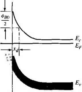 Figure 9.261 Figure for Problem 9.26. Reading List 365 9.27 A metal-semiconductor junction is formed between a metal with a work function of 43 eV and p-type sihcon with an electron affinity of 4.0 eV. The acceptor doping concentration in the sihcon is iV =5 x 10 cm~-. Assume T = 300 K. (a) Sketch the thermal equilibrium energy band diagram, (h) Determine the height of the Schottky barrier (c) Sketch the energy band diagram with an applied reverse-bias voltage ofVR =3V,{d) Sketch the energy band diagram with an applied forward-bias voltage of V = 0.25 V. 9.28 (a) Consider a metal-semiconductor junction formed between a metal with a work function of 4.65 eV and Ge with an electron affinity of 4.13 eV. The doping concentration in the Ge material is /Vj = 6 x lO- cm~ and =3 x 10 cm-. Assume T = 300 K. Sketch the zero bias energy-band diagram and determine the Schottky barrier height, (h) Repeat part (a) if the metal work function is 4.35 eV. Section 9.3 Heterojunctions 9.29 Sketch the energy-band diagrams of an abrupt Alo.:?Ga{),7 As-GaAs heterojunction for: (a) -AlGaAs, intrinsic GaAs, {h) N+-AlGaAs, p-GaAs, and (c) P+-AlGaAs, n -GaAs. Assume = 1.85 eV for AlojGaojAs and assume = A£.. 9.30 Repeat Problem 9.29 assuming the ideal electron affinity rule. Determine AEc and AE,.. *9.31 Starting with Poissons equation, derive Equation (9.48) for an abrupt heterojunction. Summary and Review *932 (a) Derive an expression for dV/dT as a function of current density in a Schottky diode. Assume the minority carrier current is negligible, (b) Compare dV/dT for a GaAs Schottky diode to that for a Si Schottky diode, (c) Compare Kj/JГ for a Si Schottky diode to that for a Si pn junction diode. 9.33 The (1/C) versus Vr data are measured for two Schottky diodes with equal areas. One diode is fabricated with 1 f-cm silicon and the other diode with 5 &2-cm silicon. The plots intersect the voltage axis as Vr = -0.5 V for diode A and at У/г = - 1.0 V for diode B. The slope of the plot for diode A is 1.5 x 10** (F-V)~ and that for diode В is 1.5 x 10 (FV) . Determine which diode has the higher metal work function and which diode has the lower resistivity silicon. *9.34 Both Schottky barrier diodes and ohmic contacts are to be fabricated by depositing a particular metal on a silicon integrated circuit. The work function of the metal is 4.5 V, Considering the ideal metal-semiconductor contact, determine the allowable range of doping concentrations for each type of contact. Consider both p- and n-type silicon regions. 9.30 Consider an n-GaAs-p-AlGaAs heterojunction in which the bandgap offsets are AEt: = 0.3 eV and AE, = 0.15 eV. Discuss the difference in the expected electron and hole currents when the junction is forward biased. READING LIST 1. Anderson, R. L. Experiments on Ge-GaAs Heterojunctions. Solid-State Electronics 5, no. 5 (September-October 1962), pp. 341-351. 2. Crowley, A- M., and S. M. Sze. Surface States and Barrier Height of Metal- Semiconductor Systems. Journal of Applied Physics 36 (1965), p. 32t2. 3. MacMillan, H. F.; H. C. Hamaker; G. E Virshup; and J. G. Werthen. Multijunction 1П-V Solar Cells: Recent and Projected Results. Twentieth IEEE Photovoltaic Specialists Conference (19S8), pp. 48-54. 4. Michaelson, H. B. Relation between an Atomic Electronegativity Scale and the Work Function. IBM Journal of Research and Development 22, no. 1 (January 1978), pp. 72-80. 5. Pierret. R. E Semiconductor Device Fundamentals. Reading, MA: Addison-Wesley, 1996. 6. Rideout, V. L. A Review of the Theory, Technology and Applications of Metal-Semiconductor Rectifiers. Thin Solid Films 4$, no. 3 (February 1, 1978), pp, 261291. 7. Roulston, D. J. Bipolar Semiconductor Devices. New York: McGraw-Hill, 1990. 8. Shur, M. Introduction to Electronic Devices. New York: John Wiley and Sons, 1996. *9. Shur, M. GaAs Devices and Circuits. New York: Plenum Press, 1987. *10. ---Physics of .Semiconductor Devices. Englewood Cliffs, NJ: Prentice Hall, 1990. Singh, J. Physics of Semiconductors and Their Heterostructures. New York: McGraw-Hill, 1993. 12. Singh, J. Semiconductor Devices: Basic Principles. New York: John Wiley and Sons, 2001. 13. Streetman, B. G and S. Banerjee. Solid State Electronic Devices. 5th ed. Upper Saddle River, NJ: Prentice Hall, 2000. 14. Sze, S. M. Physics of Semiconductor Devices. 2nd ed. New York: Wiley, 1981. *15, Wang, S- Fundamentals of Semiconductor Theory and Device Physics. Englewood Cliffs, NJ: Prentice Hall, 1989. *16. Wolfe, C. M., N. Holonyak, Jr., and G. E. Stillman. Physical Properties of Semiconductors. Englewood Cliffs, NJ: Prentice Hall, 1989. 17. Yang, E. S. Microelectronic Devices. New York: McGraw-Hill, 1988. j *18. Yuan, J. S. SiGe, GaAs, and InP Heterojunction Bipolar Transistors. New York: John Wiley and Sons, 1999. CHAPTER  The Bipolar Transistor PREVIEW The single-junction devices we have considered, including the pn homojunction diode, can be used to obtain rectifying current-voltage characteristics, and to form electronic switching circuits. The transistor is a multifunction semiconductor device that, in conjunction with other circuit elements, is capable of current gain, voltage gain, and signal-power gain. The transistor is therefore referred to as an active device whereas the diode is passive. The basic transistor action is the control of current at one terminal by voltage applied across two other terminals of the device. The three basic transistor types are the bipolar transistor, the metal-oxide-semiconductor field-effect transistor (MOSFET), and the junction field-effect transistor (JFET). The bipolar transistor is covered in this chapter, the MOSFET is treated in Chapters 11 and 12, and the JFET is discussed in Chapter 13. The chapters dealing with each of the transistor types are written to stand alone, so that each type of transistor may be covered in any order desired. The bipolar transistor has three separately doped regions and two pn junctions, sufficiently close together so that interacrions occur between the two juncrions. We will use much of the theory developed for the pn junction in the analysis of the bipolar transistor. Since the flows of both electrons and holes are involved in this device, it is called a bipolar transistor. We will first discuss the basic geometry and operation of the transistor. Since there is more than one pn junction in the bipolar transistor, several combinations of reverse- and forward-bias junction voltages are possible, leading to different operating modes in the device. As with the pn juncrion diode, minority carrier distributions in the bipolar transistor are an important part of the physics of the device-minority carrier gradients produce diffusion currents. We will determine the minority carrier distribution in each region of the transistor, and the corresponding currents. The bipolar transistor is a voltage-controlled current source. We will consider the various factors that determine the current gain and derive its mathemarical expression. As with any semiconductor device, nonideal effects influence device characteristics; a few of these effects, such as breakdown voltage, will be described. In order to analyze or design a transistor circuit, especially using computer simulations, one needs a mathematical model or equivalent circuit of the transistor. We will develop two equivalent circuits. The first equivalent circuit, the Ebers-Moll model, can be used for a transistor biased in any of its operating modes and is especially used for transistors in switching circuits. The second equivalent circuit, the hybrid-pi model, is applied when transistors are operated in a small signal linear amplifier and takes into account frequency effects within the transistor. Various physical factors affect the frequency response of the bipolar transistor. There are several time-delay factors within the device that determine the limiting frequency response. We will define these time delays and develop expressions for each factor. The limiting frequency is given in terms of a cutoff frequency, a figu of merit for the transistor. The frequency response generally applies to the s signal, steady-state characteristics of the device. The switching characteristics contrast, determine the transient behavior of the transistor to large changes in the input  10.1 I THE BIPOLAR TRANSISTOR ACTION The bipolar transistor has three separately doped regions and two pn junctions. Figure 10.1 shows the basic structure of an npn bipolar transistor and a pnp bipolar transistor, along with the circuit symbols. The three terminal connections are called the emitter, base, and collector. The width of the base region is small compared to the minority carrier diffusion length. The (++) and (+) notation indicates the relative magnitudes of the impurity doping concentrations normally used in the bipolar transistor, with (+-!-) meaning very heavily doped and (+) meaning moderately doped. The emitter region has the largest doping concentration; the collector region has the smallest. The reasons for using these relative impurity concentrations, and for the narrow base width, will become clear as we develop the theory of the bipolar transistor. The concepts developed for the pn junction apply directly to the bipolar transistor. Emitter Collector 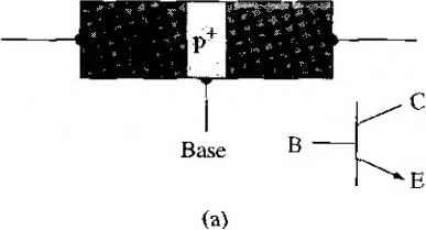 Emitter  P Collector Base В Figure lO.l I Simplified block diagrams and circuit symbols of (a) npn and (b) pnp bipolar transistors. Isolation SiOi 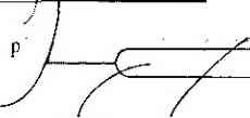 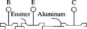 Epitaxial layer 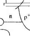 Buried Base Silicon layer substrate Conventional npn transistor Figure 10.2 i Cross section of (a) a conventional integrated-circuit npn bipolar transistor and (b) an oxide-isolated npn bipolar transistor. {From Muller and Kamins f3}.) 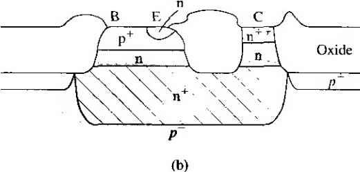 The block diagrams of Figure 10.1 show the basic structure of the transistor, but in very simplified sketches. Figure 10.2a shows a cross section of a classic npn bipolar transistor fabricated in an integrated circuit configuration, and Figure 10.2b shows the cross section of an npn bipolar transistor fabricated by a more modem technology. One can immediately observe that the actual structure of the bipolar transistor is not neariy as simple as the block diagrams of Figure 10.1 might suggest. A reason for the complexity is that terminal connecrions are made at the surface; in order to minimize semiconductor resistances, heavily doped n+ buried layers must be included. Another reason for complexity arises out of the desire to fabricate more than one bipolar transistor on a single piece of semiconductor material. Individual transistors must be isolated from each other since all collectors, for example, will not be at the same potential. This isolation is accomplished by adding p regions so that devices are separated by reverse-biased pn junctions as shown in Figure 10.2a, or they are isolated by large oxide regions as shown in Figure 10.2b. An important point to note from the devices shown in Figure 10.2 is that the bipolar transistor is not a symmetrical device. Although the transistor may contain two n regions or two p regions, the impurity doping concentrations in the einitter and collector are different and the geometry of these regions can be vastly different. The block diagrams of Figure 10.1 are highly simpfified, but useful, concepts in the development of the basic transistor theory. 10.1.1 The Basic Principle of Operation The npn and pnp transistors are complementary devices. We will develop the bipolar transistor theory using the npn transistor, but the same basic principles and equations also apply to the pnp device. Figure 10.3 shows an idealized impurity doping profile in an npn bipolar transistor for the case when each region is uniformly doped. Typical impurity doping concentrations in the emitter, base, and collector may be on the order of 10 , and 10 cm , respectively. 1 ... 34 35 36 37 38 39 40 ... 55 |
|
© 2026 AutoElektrix.ru
Частичное копирование материалов разрешено при условии активной ссылки |