 |
 |
 |
| Главная Журналы Популярное Audi - почему их так назвали? Как появилась марка Bmw? Откуда появился Lexus? Достижения и устремления Mercedes-Benz Первые модели Chevrolet Электромобиль Nissan Leaf |
Главная » Журналы » Absorbing materialorganic polymer 1 ... 35 36 37 38 39 40 41 ... 55 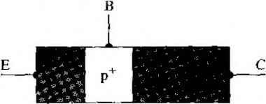 Figure 10.31 Idealized doping profile of a uniformly doped npn bipolar transistor. i The base-emitter (B-E) pn junction is forward-biased, and the base-collector (Б-С) pn junction is reverse-biased in the normal bias configuration as shown in Figure 10.4a. This configuration is called the forward-active operating mode: The B-E junction is forward-biased so electrons from the emitter are injected across the B-E junction into the base. These injected electrons create an excess concentralion of minority carriers in the base. The B-C junction is reverse biased, so the minority carrier electron concentration at the edge of the B-C junction is ideally zero. We expect the electron concentration in the base to be like that shown in Figure 10.4b. The large gradient in the electron concentration means that electrons injected from the emitter will diffuse across the base region into the B-C space charge region, where the electric field will sweep the electrons into the collector. We want as many electrons as possible to reach the collector without recombining with any majority carrier holes in the base. For this reason, the width of the base needs to be small compared with the minority carrier diffusion length. If the base width is small, then the minority carrier electron concentration is a function of both the B-E and B-C junction voltages. The two junctions are close enough to be called interacting pn junctions. Figure 10.5 shows a cross section of an npn transistor with the injection of electrons from the n-type emitter (hence the name emitter) and the collection of the electrons in the collector (hence the name collector). 10.1,2 Simplified Transistor Current Relations We can gain a basic understanding of the operation of the transistor and the relations between the various currents and voltages by considering a simplified analysis. After this discussion, we will then delve into a more detailed analysis of the physics of the bipolar transistor. The minority carrier concentrations are again shown in Figure 10.6 for an npn bipolar transistor biased in the forward active mode. Ideally, the minority carriei electron concentration in the base is a linear function of distance, which implies no j recombination. The electrons diffuse across the base and are swept into the collector by the electric field in the B-C space charge region. 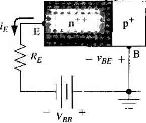 E-B space B-C space charge region charge region Emitter E-field
Collector 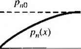 E fn) B(p) Zero bias С  Forward active Figure 10.4 I (a) Biasing of an npn bipolar transistor in the forward-active mode, (b) minority carrier distribution in an npn bipolar transistor operating in the forward-active mode, and (c) energy band diagram of the npn bipolar transistor under zero bias and under a forward-active mode bias. Collector Current Assuming the ideal linear electron distribution in the base, the collector current can be written as a diffusion current given by л гг A Пв{0)-0 0-Хв еО АвЕ (вЕ --- йоехр - 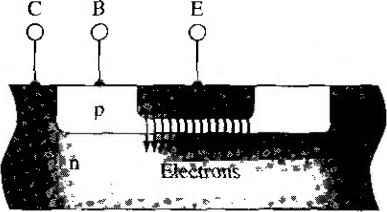 E(n) Figure 10,5 i Cross section of an npn bipolar transistor showing the injection and collection of electrons in the forward-acdve mode. B(p) ( SF s(0) = exp 1-, C(n) Ideal (linear) Actual 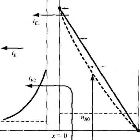 E-field  X = X в Figure 10.6 I Minority carrier distributions and basic currents in a forward-biased npn bipolar transistor where Abe is the cross-sectional area of the B-E junction, до t tbe thermal equin librium electron concentration in the base, and V, is the thermal voltage. The diffu- sion of electrons is in the -fx direction so that the conventional current is in the -jc direction. Considering magnitudes only, Equation (10.1) can be written as ic h exp (10.2) The collector current is controlled by the base-emitter voltage; that is, the current atj one terminal of the device is controlled by the voltage applied to the other two terminals of the device. As we have mentioned, this is the basic transistor action. Kmitter Current One component of emitter current, ifu sliown in Figure 10.6 is Jue to the flow of electrons injected from the emitter into the base. This current, then, equal to the collector current given by Equation (10.1). Since the base-emitter junction is forward biased, majority carrier holes in the ase are injected across the B-E juncrion into the emitter. These injected holes pro-ce a pn juncrion current iei as indicated in Figure 10.6. This current is only a B-E ction current so this component of emitter current is not part of the collector cur-nt. Since 1е2 is a forward-biased pn juncrion current, we can write (considering magnitude only) к /52expj where /52 involves the minority carrier hole parameters in the emitter. The total emitter current is the sum of the two components, or (10.3) (Vbe - (10-4) Since all current components in Equation (10.4) are functions of exp (ве/г) the ratio of collector current to emitter current is a constant. We can write - = Of (10.5) where a is called the common-base current gain. By considering Equation (10.4), we see that ic < orof < I. Since is not part of the basic transistor action, we would like this component of current to be as small as possible. We would then like the common base current gain to be as close to unity as possible. Referring to Figure 10.4a and Equarion (10.4), note that the emitter current is an exponential function of the base-emitter voltage and the collector current is ic - aif. To a first approximation, the collector current is independent of the base-collector voltage as long as the B-C junction is reverse biased. We can sketch the common-base transistor characteristics as shown in Figure 10.7. The bipolar transistor acts like a constant current source. l£4 l£2 Figure 10,71 Ideal bipolar transistor common-base current-voltage characterisfics. Base Current As shown in Figure 10.6, the component of emitter current /2 is a B-E junction current so that this current is also a component of base current sho as iBa- This component of base current is proportional to exp (v/j/ ). ** There is also a second component of base current We have considered the ideal case in which there is no recombination of minority carrier electrons with ma carrier holes in the base. However, in reality, there will be some recombin; Since majority carrier holes in the base are disappearing, they must be resuppli. a flow of positive charge into the base terminal. This flow of charge is indicated as a current iBb in Figure 10.6, The number of holes per unit time recombining in the base is directly related to the number of minority carrier electrons in the base (see Equation (6.13)). Therefore, the current ish is also proportional to exp (ve/ V), The total base current is the sum of iHa d iBh, and is proportional to exp (г'е / K). The ratio of collector current to base current is a constant since both currents directly proportional to exp (vbe/ Vr). We can then write where p is called the common-emitter current gain. Normally, the base current will be relatively small so that, in general, the common-emitter current gain is much large than unity (on the order of 100 or larger).  10,1.3 The Modes of Operation Figure 10.8 shows the npn transistor in a simple circuit. In this configuradon, tfe transistor may be biased in one of three modes of operation. If the B-E voltage is zero or reverse biased {VgE 5 0). then majority carrier electrons from the emitter will not be injected into the base. The B-C junction is also reverse biased; thus, the emitter and collector currents will be zero for this case. This condition is referred to as cutojf-d\\ currents in the transistor are zero. 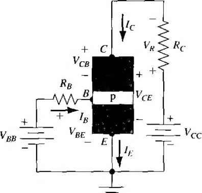 Figure 10.8 1 An npn bipolar transistor in a common-emitter circuit configuration. When the B-E junction becomes forward biased, an emitter current will be generated as we have discussed, and the injection of electrons into the base results in a collector current. We may write the КVL equations around the collector-emitter loop as Vcc = IcRc + Уев + Vnt: = + Усе (10.7) If Усе is large enough and if Vr is small enough, then Уев > 0, which means that the B-C junction is reverse biased for this npn transistor. Again, this condition is the forward-active region of operation. As the forward-biased B-E voltage increases, the collector current and hence У^ will also increase. The increase in Vr means that the reverse-biased C-B voltage decreases, or Vcs I decreases. At some point, the collector current may become large enough that the combination of Vr and Усе produces zero voltage across the B-C junction. A slight increase in I с beyond this point will cause a slight increase in Vr and the B-C junction will become forward biased (Уев < 0). This condition is called saturation. In the saturation mode of operation, both B-E and B-C junctions are forward biased and the collector current is no longer controlled by the B-E voltage. Figure 10.9 shows the transistor current characteristics, Ic versus Vce-, for constant base currents when the transistor is connected in the common-emitter configuration (Figure 10.8). When the collector-emitter voltage is large enough so that the base-collector junction is reverse biased, the collector current is a constant in this first-order theory. For small values of C-E voltage, the base-collector junction becomes forward biased and the collector current decreases to zero for a constant base current. Writing a Kirchhoffs voltage equation around the C-E loop, we find Усе - Усе hc (10.8) Equafion (10.8) shows a linear relation between collector current and collector-emitter voltage. This linear relation is called a load line and is plotted in Figure 10.9. The load line, superimposed on the transistor characteristics, can be used to visualize the bias condition and operating mode of the transistor. The cutoff mode occurs when Saturation 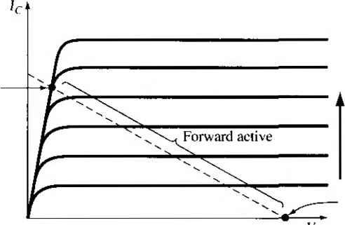 Increasing Ib Cutoff Figure 10.9 j Bipolar transistor common-emitter current-voltage characteristics with load line superimposed.  = 0, saturation occurs when there is no longer a change in collector current for change in base current, and the forward-active mode occurs when the relati - pis is valid. These three operating modes are indicated on the figure. A fourth mode of operation for the bipolar transistor is possible, although with the circuit configuration shown in Figure 10.8. This fourth mode, known as inverse active, occurs when the B-E junction is reverse biased and the B-C junction is forward biased. In this case the transistor is operating upside down, and the roles of the emitter and collector are reversed. We have argued that the transistor is not a symmetrical device; therefore, the inverse-active characteristics will not be the same as the forward-active characteristics. The junction voltage conditions for the four operating modes are shown in Figure 10,10. 10ЛД Amplification with Bipolar Transistors Voltages and currents can be amplified by bipolar transistors in conjunction wit other elements. We will demonstrate this amplification qualitatively in the followinj discussion. Figure 10Л1 shows an npn bipolar transistor in a common-etnitter C( figuration. The dc voltage sources, Уцв and Vc, are used to bias the transistor in the forward-active mode. The voltage source ь', represents a time-vary ing input voltage (such as a signal from a satellite) that needs to be amplified. Figure 10.12 shows the various voltages and currents that are generated in the circuit assuming that is a sinusoidal voltage. The sinusoidal voltage induces a sinusoidal component of base current superimposed on a dc quiescent value. Since i fiif. then a relatively large sinusoidal collector current is superimposed on a dc value of collector current. The dme-varying collector current induces a time-varying voltage across the Rc resistor which, by Kirchhoffs voltage law, means that a sinusoidal voltage, superimposed on a dc value, exists between the collector and emitter of the bipolar transistor. The sinusoidal voltages in the collector-emitter
Figure 10,10 I Junction voltage conditions for the four operating modes of a bipolar transistor. в 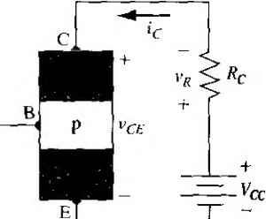 Figure 10,11 1 Common-emitter npn bipolar circuit configuration with a time-vary ing signal voltage Vj included in the base-emitter loop.  Current 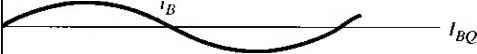 Figure 10.12 I Currents and voltages existing in the circuit shown in Figure lO.lL (a) Input sinusoidal signal voltage, (b) Sinusoidal base and collector currents superimposed on the quiescent dc values, (c) Sinusoidal voltage across the resistor superimposed on the quiescent dc value. portion of the circuit are larger than the signal input voltage v so that the circuit has produced a voltage gain in the time-varying signals. Hence, the circuit is known as a voltage amplifien In the remainder of the chapter, we will consider the operation and characteristics of the bipolar transistor in more detail. 10.2 I MINORITY CARRIER DISTRIBUTION We are interested in calculating currents in the bipolar transistor which, as in the simple pn junction, are determined by minority carrier diffusion. Since diffusion currents are produced by minority carrier gradients, we must determine the steady-state Table 10Л I Notation used in the analysis of the bipolar transistor Notation Definition For both the npn and pnp transistors Doping concentradons in the emitter, base, and collector Widths of neutral emitter, base, and collector regions Minority carrier diffusion coefficients in emitter, base, and collector regions Minority carrier diffusion lengths in emitter, base, and collector regions Minority carrier lifefimes in emitter, base, and collector regions xexs,xc De.DsDc For the npn />£0. ПвО^ PCi) Ре{х'),пв{х). Pcix ) SpEix), 8пв{х)Лрс{х ) For the pnp пео, Рво-> пс[] пе{х'). рв{х),пс{х ) 6пе(х'),6рв (х),8пс(х') Thermal equilibrium minority carrier hole, electron, and hole concentrafions in the emitter, base, and collector Total minority carrier hole, electron, and hole concentrations in the emitter base, and collector Excess minority carrier hole, electron, and hole concentrations in the cmiUer, base, and collector Thermal equilibrium minority carrier electron, hole, and electron concentrations in the emitter, base, and collector Total minority carrier electron, hole, and electron concentrations in the emitter, base, and collector Excess minority carrier electron, hole, and electron concentrations in the emitter, base, and collector Emitter Base Collector
х=ле x=Ox = 0 xxbx* = 0 X - Xf Figure 10ЛЗ I Geometry of the npn bipolar transistor used to calculate the minority carrier distribution. minority carrier distribution in each of the three transistor regions. Let us first consider the forward-active mode, and then the other modes of operation. Table 10.1 suimarizes the notation used in the following analysis. 10ЛЛ Forward-Active Mode Consider a uniformly doped npn bipolar transistor with the geometry shown in Figure 10.13. When we consider the individual emitter, base, and collector regions, we
Figure 10.14 I Minority carrier distribution in an npn bipolar transistor operating in the forward-active mode. will shift the origin to the edge of the space charge region and consider a positive x, x\ or x coordinate as shown in the figure. In the forward-active mode, the B-E junction is forward biased and the B-C is reverse biased. We expect the minority carrier distributions to look like those shown in Figure 10.14. As there are two n regions, we will have minority carrier holes in both emitter and collector. To distinguish between these two minority carrier hole distrib-ufions, we will use the notation shown in the figure. Keep in mind that we will be dealing only with minority carriers. The parameters pto, пво, and pco denote the thermal-equilibrium minority carrier concentrations in the emitter, base, and collector, respectively. The functions pe{x), пв(х), and pcUO denote the steady-state minority carrier concentrations in the emitter, base, and collector, respectively. We will assume that the neutral collector length xc is long compared to the minority carrier diffusion length Lc in the collector, but we will take into account a finite emitter length xe. If we assume that the surface recombination velocity at x = xe is infinite, then the excess minority carrier concentration at = xe is zero, or p£(x = xe) = pEQ. An infinite surface recombination velocity is a good approximation when an ohmic contact is fabricated at x = xe- Base Region The steady-state excess minority carrier electron concentrarion is found from the ambipolar transport equation, which we discussed in detail in Chapter 6- For a zero electric field in the neutral base region, the ambipolar transport equation in steady state reduces to дН8пв{х)) 8пв(х) (10.9) where 8пв is the excess minority carrier electron concentration, and Db and ro are the minority carrier diffusion coefficient and lifetime in the base region, respectively. The excess electron concentration is defined as Snfi(x) = Пв(х) - ПВО (10.10) 1 ... 35 36 37 38 39 40 41 ... 55 |
|||||||||||||||||||||||||||||||||||||||||||||||||||||||||||||||||||||||||||||||||||||||||||||
|
© 2026 AutoElektrix.ru
Частичное копирование материалов разрешено при условии активной ссылки |