 |
 |
 |
| Главная Журналы Популярное Audi - почему их так назвали? Как появилась марка Bmw? Откуда появился Lexus? Достижения и устремления Mercedes-Benz Первые модели Chevrolet Электромобиль Nissan Leaf |
Главная » Журналы » Absorbing materialorganic polymer 1 ... 36 37 38 39 40 41 42 ... 55 The general solution to Equation (10,9) can be written as 8пв(х) = Л exp + exp where is the minority carrier diffusion length in the base, given by Lb = /DiZBb The base is of finite width so both exponential terms in Equation (lO.U) must be retained. The excess minority carrier electron concentrations at the two boundaries become 8пв(х =0)=6пвФ) A+ В (10Л2а) Snsix - Xp) = Ьпв(хв) - A exp + exp (10.12b) The B-E junction is forward biased, so the boundary condition at л = 0 is пвФ)пв(х^О)~пв-пв expj-l (ЮЛЗа) The B-C junction is reverse biased, so the second boundary condition at jc = is SngixB) - пв(х =xb) -пва = 0- пва = - eo (ЮЛЗЬ) From the boundary conditions given by Equations (10.13a) and (10.13b), the coefficients A and В from Equations (10.12a) and (10.12b) can be determined. The results are в 2 sinh ( (10Л4а) ПВО -(e) (10.14b) 2 sinh Then, substituting Equations (10.14a) and (10.14b) into Equation (10.9), we can write the excess minority carrier electron concentration in the base region as 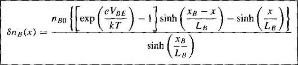 .15a] Mr L2 1.0 0.6 0,4 - 0.2 - sinh (y) Linear 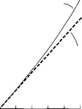 approxmiation 0 0.2 0.4 0.6 0.8 LO 1.2 Figure 10.15 I Hyperbolic sine function and its linear approximation. Equation (10.15a) may look formidable with the sinh functions. We have stressed that we want the base width хв to be small compared to the minority carrier diffusion length Lв This condition may seem somewhat arbitrary at this point, but the reason will become clear as we proceed through all of the calculations. Since we want хи < Lb, the argument in the sinh functions is always less than unity and in most cases will be much less than unity. Figure 10,15 shows a plot of sinh (v) for 0 < у < 1 and also shows the linear approximation for small values of y. If у < 0.4, the sinh (y) function differs from its linear approximation by less than 3 percent. All of this leads to the conclusion that the excess electron concentration Sn in Equation (lOJSa) is approximately a linear function of x through the neutral base region. Using the approximation that sinh (jc) x for x <K 1, the excess electron concentration in the base is given by (10.15b) 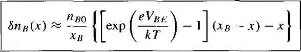 We will use this linear approximation later in some of the example calculations. The difference in the excess carrier concentrations determined from Equations (10.15a) and (10.15b) is demonstrated in the following exercise. TEST YOUR UNDERSTANDING ElO.l The emitter and base of a silicon npn bipolar transistor are uniformly doped at impurity concentrations of 10 cm - and 10 cm , respectively. A forward-bias B-E voltage of Vf 0.610 V is applied. The neutral base width is л в =:2pm and the minority carrier diffusion length in the base is 1ц - 10 m. Calculate the excess minority carrier concentration in the base at (a) x = 0 and (h) x = хц/2, (с) Determine the ratio of the actual minority carrier concentration at jc = xs/2 (Equation (10Л5а)) to that in the ideal case of a hnear minority carrier distribution (Equation (t0.l5b)>. [О^ббО = (tiOl x l706-l/t ai x СШ\) PiH P) Ч-шэ ,01 x = (Z/x)u {1/х)щ {q) Ч-и01 X (o) w(r?)suvl Table 10.2 shows the Taylor expansions of some of the hyperbolic functions will be encountered in this section of the chapter. In most cases, we will consi( only the linear terms when expanding these functions. Emitter Region Consider, now, the minority carrier hole concentration in the emit ter. The steady-state excess hole concentration is determined from the equation - = 0 (10.161 where Dt and г£о are the minority carrier diffusion coefficient and minority carriei lifetime, respectively, in the emitter. The excess hole concentration is given by PeW) = pe(x) - Peo (10.17) The general solution to Equation (10.16) can be written as Spt(x) - С exp (~ + exp (j (10Л8) where = \/£>T£o. If we assume the neutral emitter length xe is not necessarily j long compared to L. then both exponential tenns in Equation (10.18) must be retained. The excess minority carrier hole concentrations at the two boundaries are Spe(x > 0) = SpEiO) = C + D (10.19a) Sptix = xe) - Spe(xe) - Cexp I ~] + Л exp у ~) (-b) Table 10.2 1 Taylor expansions of hyperbolic functions Function Taylor expansion
igain, the B-E junction is forward biased so <5/?e(0) - pf(x = 0) - Peo = Peo (10.20a) [An infinite surface recombination velocity aix - xe implies that 8pe{xe) - 0 (10.20b) Solving for С and D using Equations (10.19) and (10.20) yields the excess minority carrier hole concentrarion in Equation (10.18): 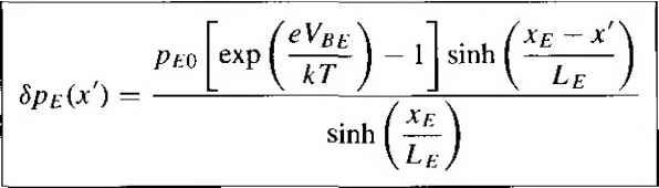 (10.21a) This excess concentration will also vary approximately linearly with distance i/xe is small We find 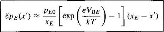 (10.21b) Uxe is comparable to Lf, then bpix) shows an exponential dependence on jc£. TEST YOUR UNDERSTANDING E10.2 Consider a silicon npn bipolar transistor with emitter and base regions uniformly L doped at concentrations of lO cm~ and 10 cm *, respecfively. A forward bias г B-E voltage of Vbe = 0.610 V is applied. The neutral emitter width is xe = 4 дт and the minority carrier diffusion length in the emitter is =4 дт. Calculate the excess minority carrier concentration in the emitter at (o) jc 0 and {b)x = xe /2. U- ciOl x 689T () etOI Ш'г W *suvl Collector Region The excess minority carrier hole concentration in the collector can be determined from the equarion д\Ьрс{х')) ЬрсХх') О (10.22) where Dc and тсо are the minority carrier diffusion coefficient and minority carrier lifefime, respectively, in the collector. We can express the excess minority carrier hole concentration in the collector as Pcix) pcix ) - Pco (10.23) The general solution to Equation (10.22) can be written as bpc{x) - О exp И exp where Lc л/Оссо- If we assume that the collector is long, then the coefficient must be zero since the excess concentration must remain finite. The second bourn condhion gives Spcix = 0) = SpciO) pc(x 0) - pco = 0- pci) - -pco (10.: The excess minority carrier hole concentration in the collector is then given as Pc(x) = -/?coexp (- j (10.2( This resuh is exactly what we expect from the results of a reverse-biased pn juncti( TEST YOUR UNDERSTANDING E10.3 Consider the collector region of an npn bipolar transistor biased in the forward ac-five region. At what value of л , compared to Lc. does the magnitude of the minority carrier concentration reach 95 percent of ihe thermal equilibrium value. 10.2,2 Other Modes of Operation The bipolar transistor can also operate in the cutoff, saturation, or inverse-active mode. We will qualitarively discuss the minority carrier distributions for these operating conditions and treat the actual calculations as problems at the end of the chapter. Figure 10.16a shows the minority carrier distriburion in an npn bipolar transis-: tor in cutoff. In cutoff, both the B-E and B-C junctions are reverse biased; thus, the Emitter -n-  Base 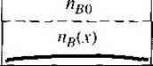 Collector -n- 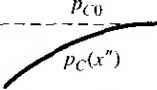
Figure 10.16 I Minority carrier distribution in an npn bipolar transistor operating in (a) cutoff and (b) saturation.  Base -P- 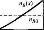 CoUector 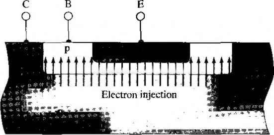 Figure 10Л7 I (a) Minority carrier distribution in an npn bipolar transistor operating in the inverse-active mode, (b) Cross section of an npn bipolar transistor showing the injection and collection of electrons in the inverse-active mode. minority carrier concentrations are zero at each space charge edge. The emitter and collector regions are assumed to be long in this figure, while the base is narrow compared with the minority carrier diffusion length. Since jc <$C Lb, essentially all minority carriers are swept out of the base region. Figure 10.16b shows the minority carrier distribution in the npn bipolar transistor operating in saturation. Both the B-E and B-C junctions are forward biased; thus, excess minority carriers exist at the edge of each space charge region. However, since a collector current still exists when the transistor is in saturation, a gradient will still exist in the minority carrier electron concentration in the base. Finally, Figure 10.17a shows the minority carrier distribution in the npn transistor for the inverse-active mode. In this case, the B-E is reverse biased and the B-C is forward biased. Electrons from the collector are now injected into the base. The gradient in the minority carrier electron concentration in the base is in the opposite direction compared with the forward-active mode, so the emitter and collector currents will change direction. Figure 10J7b shows the injecrion of electrons from the collector into the base. Since the B-C area is normally much larger than the B-E area, not all of the injected electrons will be collected by the emitter. The relative doping concentrations in the base and collector are also different compared with those in the base and emitter; thus, we see that the transistor is not symmetrical. We then expect the characteristics to be significanriy different between the forward-active and inverse-active modes of operation. 10.3 t LOW-FREQUENCY COMMON-BASE CURRENT GAIN The basic principle of operation of the bipolar transistor is the control of the collector current by the B-E voltage. The collector current is a function of the number of majority carriers reaching the collector after being injected from the emitter across file B-E junction. The common-base current gain is defined as the ratio of collector current to emitter current. The flow of various charged carriers leads to definitions of   particular currents in the device. We can use these definitions to define the current gain of the transistor in terms of several factors. 10<3.1 Contributing Factors Figure 10.18 shows the various particle flux components in the npn bipolar transistor. We will define the various flux components and then consider the resulting currents. Although there seems to be a large number of flux components, we may help clarify the situation by correlating each factor with the minority carrier distribul shown in Figure 10.14. The factor J, is the electron flux injected from the emitter into the base. As electrons diffuse across the base, a few will recombine with majority carrier ho! The majority carrier holes that are lost by recombination must be replenished from the base terminal. This replacement hole flux is denoted by Jj. The electron flux that reaches the collector is J~. The majority carrier holes from the base that arc injected back into the emitter result in a hole flux denoted by . Some electrons and holes that are injected into the forward-biased B-E space charge region will recombine in this region. This recombination leads to the electron flux J. Generation of electrons and holes occurs in the reverse-biased B-C junction. This generation yields a hole flux J. Finally, the ideal reverse-saturation cuirent in the B-C junction is denoted by the hole flux J. I The corresponding electric current density components in the npn transistor atTtl shown in Figure 10.19 along with the minority carrier distributions for the forward-; active mode. The curves are the same as in Figure 10.14. As in the pn junction, die currents in the bipolar transistor are defined in terms of minority carrier diffusi( currents. The current densities are defined as follows; Due to the diffusion of minority carrier electrons in the base at jc = 0, Jnc. Due to the diffusion of minority carrier electrons in the base at x ~хв- JjiB The difference between Je and i c. which is due to the recombination of excess minority carrier electrons with majority carrier holes in the base. The JfiB current is the flow of holes into the base to replace the holes lost by recombination. Jp£: Due to the diffusion of minority carrier holes in the emitter at j: 0. 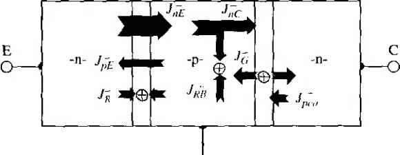 Figure 10.181 Particle current density or flux components in an npn bipolar transistor operating in the forward-active mode. Emitter -n- 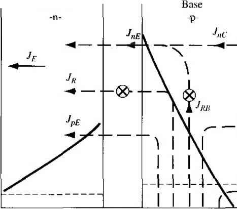 X = Xe x = 0 x = 0 Collector с 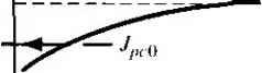 Figure 10.19 I Current density cotnponents in an npn bipolar transistor operating in the forward-active mode. Jr: Due to the recombination of carriers in the forward-biased B-E junction. Jpco: Due to the diffusion of minority carrier holes in the collector at jc =0. Ja: Due to the generation of carriers in the reverse-biased B-C juncrion. The currents Jrb jpe <ind Jr are B-E juncrion currents only and do not contribute to the collector current. The currents J.o and Jq are B-C junction currents only. These current components do not contribute to the transistor action or the current gain. The dc common-base current gain is defined as (10.27) If we assume that the acrive cross-sectional area is the same for the collector and emitter, then we can write the current gain in terms of the current densiries, or Go = - =---7 (10.28) Je jne + jrjpe We are primarily interested in determining how the collector current will change with a change in emitter current. The small-signal, or sinusoidal, common-base current gain is defined as Э jr jn с oJe jfie + + JpE The reverse-bias B-C currents, Jg and Jpo, are not functions of the emitter current. We can rewrite Equation (10.29) in the form ( JnE \(J}C\( JnE + JpE \ \JnE\rJpE)\JnE)\JnE + JR + JpE) a = yar (10.! The factors in Equation (10.30b) are defined as: y - {--J = emitter injection efficiency factor (10.31; ar ( - ) = base transport factor (10.311 8 = -{±J±- recombination factor (10.31c] We would like to have the change in collector current be exactly the same as change in emitter current on ideally, to have a - \, However, a consideration < Equation (10.29) shows that a will always be less than unity. The goal is to make as close to one as possible. To achieve this goal, we must make each term in Eq> tion (10.30b) as close to one as possible, since each factor is less than unity. The emitter injection efficiency factor у takes into account the minority car hole diffusion current in the emitter. This current is part of the emitter current, but] does not contribute to the transistor action in that JpE is not part of the collector cur-] rent. The base transport factor ar takes into account any recombination of ex< minority carrier electrons in the base. Ideally, we want no recombination in the base.] The recombination factor S takes into account the recombination in the forward-biased B-E junction. The current Jr contributes to the emitter current, but does not) contribute to collector current, 10.3.2 Mathematical Derivation of Current Gain Factors We now wish to determine each of the gain factors in terms of the electrical geometrical parameters of the transistor. The results of these derivations will show how the various parameters in the transistor influence the electrical properties of the device and will point the way to the design of a good* bipolar transistor. Emitter Injection Efficiency Factor Consider, initially, the emitter injection efficiency factor. We have from Equation (10.31a) 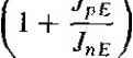 We derived the minority carrier distribution functions for the forward-active mode in Section 10.2.1. Noting that J e as defined in Figure 10.19, is in the negative fjf direction, we can write the current densities as JpE = -eDE (10.33a) JnE = (-)еОв djSnBJx)) dx (10.33b) jc = 0 where Spe(x) and 8пв(х) are given by Equations (10.21) and (10.15), respectively. Taking the appropriate derivatives of Spix) and Зпв(х), we obtain eDEPEO tanh (xe/Le) (10.34a) JiiE = sinh (xb/Lb) [ехр{еУвЕ/кТ)-\] tanh (xb/Lb) (10.34b) Positive JpE and values imply that the currents are in the directions shown in Figure 10.19. If we assume that the B-E junction is biased sufficiently far in the forward bias so that Vbe кТ/е, then and also txp{eVBE/lcT) tanh (xb/Lb) sinh (xb/Lb) The emitter injection efficiency, from Equation (10.32), then becomes PeqDeLb tanh(xB/Ls) пвоОвЬе tanh (xe/Le) (10.35a) If we assume that all the parameters in Equation (10.35a) except peo and n bo are fixed, then in order for у 1, we must have po <K во- We can write ± ПВО where Ne and Л^ are the impurity doping concentrarions in the emitter and base, re-specrively. Then the condition that /?£o < во imphes that Nb* For the emit- ter injection efficiency to be close to unity, the emitter doping must be large compared to the base doping. This condition means that many more electrons from the n-type emitter than holes from the p-type base will be injected across the B-E space 1 ... 36 37 38 39 40 41 42 ... 55 |
|
© 2026 AutoElektrix.ru
Частичное копирование материалов разрешено при условии активной ссылки |