 |
 |
 |
| Главная Журналы Популярное Audi - почему их так назвали? Как появилась марка Bmw? Откуда появился Lexus? Достижения и устремления Mercedes-Benz Первые модели Chevrolet Электромобиль Nissan Leaf |
Главная » Журналы » Absorbing materialorganic polymer 1 ... 37 38 39 40 41 42 43 ... 55 charge region. If both < Lb and x 4C Le then the emitter injection efficienc\ can be written as
(10.31 Base Transport Factor The next term to consider is the base transport faciov. given by Equation (10.31b) as aj ~ Jnc/JnE- From the definitions of the cuneni directions shown in Figure 10.19, we can write (1(6пв(х)) dx (10.36a X =X8 djbnBJx)) dx (10.36hi Using the expression for 8пв{х) given in Equation (10.15), we find that в [ехр(У^я/П-1] sinh (xb/Lb) tanh (xb/L (10.37) The expression for Je was given in Equarion (10.34a). If we again assume that the B-E junction is biased sufficiently far in the forwaru bias so that Vbe кТ/е, then ехр{еУвЕ/T) E Substituting Equations (10.37j and (I0.34b) into Equation (10.31 b), we have lc exp(eVBe/fL) +coshixB/LB) Je 1 + exp {cVbe/L) cosh (xb/Lr) (10.38) In order for ar to be close to unity, the neutral base width хв must be much smaller than the minority earner diffusion length in the base L/j. If лв <$C then! сонЪ(хв/Ев) will be just slightiy greater than unity. In addition, if ехр(1/л£/ кТ) \ , then the base transport factor is approximately (I0.39a) 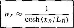 For x < Lb, may expand the cosh function in a Taylor series, so that 1 1 1 - ar =-- -- 1--(xh/Lfi) coshixB/LB) IUxb/Lb) 2 (10.39b) The base transport factor ar will be close to one if x/ Л/?. We can now see why we indicated earlier that the neutral base width Хв would be less than L. Recom bination Factor The recombination factor was gi ven by Equation (10.31c). We can write JnE + JpE J.E I JnE ~ Jr JpE JnE Jr 1 + JrI JnE We have assumed in Equation (10.40) that JpE < JnE- The recombination current density, due to the recombination in a forward-biased pn junction, was discussed in ; Chapter 8 and can be written as , ехвкЩ Jr = - where xjr is the B-E space charge width. The current JnE ffom Equation (10.34b) can be approximated as Л£-Лоехр( (10.42) where еОвПво /in Lb tanh (xb/Lb) The recombination factor, from Equation (10.40), can then be written as 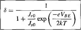 (10.44) The recombination factor is a function of the B-E voltage. As Vbe increases, the recombination current becomes less dominant and the recombination factor approaches unity. The recombination factor must also include surface effects. The surface effects can be described by the surface recombination velocity as we discussed in Chapter 6. Figure 10.20a shows the B-E junction of an npn transistor near the semiconductor surface. We will assume that the B-E junction is forward biased. Figure 10.20b shows the excess minority carrier electron concentration in the base along the cross section A-A. This curve is the usual forward-biased junction minority carrier concentration. Figure 10.20c shows the excess minority carrier electron concentration along the cross section C-C from the surface. We showed earlier that the excess concentration at a surface is smaller than the excess concentration in the bulk material. With this electron distribution, there is a diffusion of electrons from the bulk toward the surface where the electrons recombine with the majority carrier holes. Figure 10.20d shows the injection of electrons from the emitter into the base and the diffusion of electrons toward the surface. This diffusion generates another component of recombination current and this component of recombination current must be included in the recombination factor 8. Although the actual calculation is difficult because of the two-dimensional analysis required, the form of the recombination current is the same as that of Equation (10.41). С  С  Diffusion of electrons С Surface 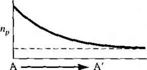 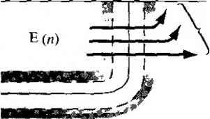 Flow of I ekctw Figure 10.20 i The surface at the E В junction showing the diffusion of carriers toward the surface. 10*3,3 Summary Although we have considered an npn transistor in all of the derivations, exactly the same analysis applies to a pnp transistor; the same minority carrier distributions will be obtained except that the electron concentrations will become hole concentrations and vice versa. The current directions and voltage polarities will also change. We have been considering the common-base current gain, defined in Equarion (10.27) as ao - Ic/h- The common-emitter current gain is defined as = icIH- From Figure 10.8 we see that /£ iв ean determine the relation between common-emitter and common-base current gains from the KCL equafion. We can write + 1 /с к Substituting the definitions of current gains, we have 1 1 - - + 1 ofo Po Since this relation actually holds for both dc and small-signal conditions, we can drop the subscript. The common-emitter current gain can now be written in terms of the common-base current gain as The common-base current gain, in terms of the common-emitter current gain, is found to be Table 10.3 I Summary of limiting factors Emitter injection efficiency (-v Eb).Ue Le) Ne Db xe Base transport factor r ---{xb < La) Recombination factor Common-base current gain ra = yajS -~---~----г- --- Db xe 2\Lb) Ло \ 2кТ ) Common-emitter current gain Ne Db Д 2 U J Ло V 2kT Table 10.3 summarizes the expressions for the limiting factors in the common base current gain assuming that хв < L and xe <K L, Also given are the approximate expressions for the common-base current gain and the common-emitter current gain. 10.3.4 Example Calculations of the Gain Factors If we assume a typical value of to be 100, then a - 0.99. If we also assume that у = ат = then each factor would have to be equal to 0.9967 in order that j6 = 100. This calculation gives an indication of how close to unity each factor must be in order to achieve a reasonable current gain. Objective I design example 10.1 To design the ratio of emitter doping to base doping in order to achieve an emitter injection efficiency factor equal to у = 0.9967. Consider an npn bipolar transistor Assume, for simplicity, that D Db. e ~ L, and xe = xf}.  у = -= 0,9967 1 + - Then - - 0.00331 or - = 302 m Comment The emitter doping concentration must be much larger than the base doping concentration achieve a high emitter injection efficiency. DESIGN Objective EXAMPLE 10.2  To design the base width required to achieve a base transport factor equal to 0.9967. Consider a pnp bipolar transistor. Assume that Db = Ю cm/s and rfo = I0~ s. Solution The base transport factor applies to both pnp and npn transistors and is given by ax =- = 0.9967 С0511(Лв/Ьв) Then xb/Lb =0.0814 We have Lb - л/аТйо - ч/(10)(10-) = 10 cm so that the base width must then be xb = 0.814 X 10 cm = 0.814 дт Ш Comment If the base width is less than approximately 0.8 дт, then the required base transport facta will be achieved. In most cases, the base transport factor will not be the limiting factor in thi bipolar transistor current gain. Solution Equation (10.35a) reduces to Objective To calculate the torward-biased B-E voUage required to achieve a recombination factor equal to 6 =0.9967. Consider an npn bipolar transistor at 7 = 300 K. Assume that Ли = Ю A/cm- and that 7,0 =10- AW. Solution The recombination factor, from Equation (10.44), is example 10.3 We then have , Ло f-eV 1 -h exp 2кТ ) 0.9967 = 10- f-eVsE 1 + T-rr exp We can rearrange this equation and write (+еУвЕ\ 0.9967 x 10- \~2k7) ~ I - 0.9967 = 3.02 x 10 Then Vbe = 2(0.0259) In{3.02 x 10) = 0.654 V Comment This example demonstrates that the recombination factor may be an important limiting factor in the bipolar current gain. In this example, if Vbe is smaller than 0.654 V, then the recombination factor S will fall below the desired 0.9967 value. Objective] example io.4 To calculate the common-emitter current gain of a silicon npn bipolar transistor at Г = 300 К given a set of parameters. Assume the following parameters: lOcm/s Db = 25 cmVs ro = 1 x 10 s tbo = 5 x 10 s 5 x 10 A/cm xb = 0.70 дт xe = 0.50 дт Ne = 1 x 10 cm jV = 1 x 10 cm Vbe = 0.65 V The following parameters are calculated: (1.5 X 10<) 3 0 = -r-TTZ- = 2-5 X 10 cm 1 X 10 (1.5 X 10°) 4 3 2.25 X 10 cm 1 X 10 Le = y/OtZEo = 10 cm Lb - VL>btbq = 3.54 x 10 cm Solution The emitter injection efficiency factor, from Equation (10.35a), is (2.25 X 10)(10)(3.54 x 10 ) tanh(0.0198) = 0.9944 (2.25 X im)(25)(10-) tanh (0.050) The base transport factor, from Equation (10.39a) is , /0.70 X 10- cosh i -- V3.54 X 10- The recombinafion factor, from Equafion (10.44), is = 0.9998 5x10- / -0.65 \ V 2(0.0259) j where Jsi) = L s tanh (1.6 X 10-)(25)(2.25 X 10) 3.54 X 10-Manh (1.977 x 10 ) 1.29 X ]0-A/cm We can now calculate 8 = 0.99986. The common-base current gain is then ayarS = (0.9944) (0.9998) (0.99986) = 0.99406 which gives a common-emitter current gain of a 0.99406 1 - fl 1 0.99406 Comment In this example, the emitter injection efficiency is the limifing factor in the current gain. TEST YOUR UNDERSTANDING NOTE: In Exercises El0.4 through El0.9, assume a silicon npn bipolar transistor at Г = 300К has the following minority carrier parameters: De = 8cm/s, Dn = 20cmVs, Dc 12cmVs, teo = 10 s, tbo 10- s, Tci) = 10- s. E10.4 If the emitter doping concentration isJVг = 5xl0cm , find the base doping concentration such that the emitter injection efficiency is у = 0.9950. Assume ElO.S Assume that ат = S = 0.9967, xs = x = I дт, Л^й = 5 x 10 cm- and Ne 5 X 10 cm-\ Determine the common emitter current gain 9. (£Z6 - suy) Е10.6 Determine the minimum base width Хв such that the base transport factor is ar = 0.9980. (ш^ 568*0 = *suv) Е10.7 Assume that у = S = 0.9967 and xg = 0.80 дт. Determine the common-emitter current gain/3. {\Z\ = suv) Е10.8 If Ло = 10 * A/cm and Ло = 10 A/cm find the value of Vbe such that S = 0.9960. (A 9ei790 = A Е10.9 As.sume that у aj = 0.9967, Ло = 5 x 10 A/cm J,o = lO A/cm\ and Vbe = 0.585 V. Determine the common-emitter current gain p. (VLL= suy) 10.4 I NONIDEAL EFFECTS In all previous discussions, we have considered a transistor with uniformly doped regions, low injection, constant emitter and base widths, an ideal constant energy bandgap, uniform current densities, and junctions which are not in breakdown. If any of these ideal conditions are not present, then the transistor properties will deviate from the ideal characteristics we have derived. 10.4Л Base Width Modulation We have implicitly assumed that the neutral base width хв was constant. This base width, however, is a function of the B-C voltage, since the width of the space charge region extending into the base region varies with B-C voltage. As the B-C reverse-bias voltage increases, the B-C space charge region width increases, which reduces jr. A change in the neutral base width will change the collector current as can be observed in Figure 10.21. A reduction in base width will cause the gradient in the minority carrier concentration to increase, which in turn causes an increase in the diffusion current. This effect is known as base width modulation; it is also called the Early effect. The Early effect can be seen in the current-voltage characteristics shown in Figure 10.22. In most cases, a constant base current is equivalent to a constant B-E voltage. Ideally the collector current is independent of the B-C voltage so that the slope of the curves would be zero; thus the output conductance of the transistor would be zero. However, the base width modulation, or Early effect, produces a nonzero slope and gives rise to a finite output conductance. If the collector current characteristics are extrapolated to zero collector current, the curves intersect the voltage axis at a point that is defined as the Early voltage. The Early voltage is considered to be a positive value. It is a common parameter given in transistor specifications; typical values of Early voltage are in the 100- to 300-volt range. 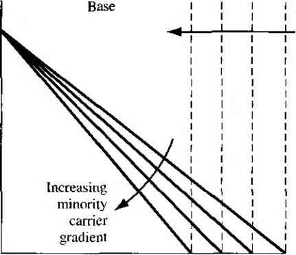 Moving space charge edge with increasing C-B voltage x = 0 X = X. Figure 10.211 The change in the base width and the change in the minority carrier gradient as the B-C space charge width changes. 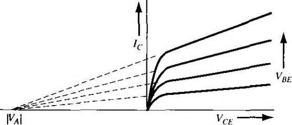 Figure 10.22 I The collector current versus collector-emitter voltage showing the Early effect and Early voltage. From Figure 10.22, we can write that die Ic VcE + Va (10.4! where and Vc e are defined as positive quantities and go is defined as the out conductance. Equation (10.45a) can be rewritten in the form 1с=8о(Усе + Уа) (10.45b) showing explicitly that the collector current is now a function of the C-E voltage or the C-B voltage. Objective To calculate the change in the neutral base width with a change in C-B voltage. Consider a uniformly doped silicon bipolar transistor at T = 300 К with a base doping of Ns = 5 X \0 cm and a collector doping of Л^с =2 x IO cm~\ Assume the metallurgical base width is 0.70 /xm. Calculate the change in the neutral base width as the C-B voltage cbanges from 2 to 10 V. Solution The space charge width extending into the base region can be written as X,tB = с XiiB - 2(lL7}(8.85x \0-)(Уь,+Усв) 1.6 x 10- 2 X 10 5 x 10 (5 x 10+2 x 10⁵ which becomes х,в={{9.9вх[0~){Уы + Усв)] The buih-in potential is У NbNc 0.718 V For VcB = 2 V, we find x = 0.052 дт, and for Vc = Ю V, we find х^в = 0.103 дт. If we neglect the B-E space charge region, which will be small because of the forward-biased junction, then we can calculate the neutral base width. For Vcb =2 V. xb = 0.70 - 0.052 = 0.648 дт and for Vcb = Ю V, xb = 0.70 - 0.103 = 0.597 дт Comment This example shows that the neutral base width can easily change by approximately 8 percent as the C-B voltage changes from 2 to 10 V. Objective EXAMPLE io.6 To calculate the change in collector current with a change in neutral base width, and to estimate the Early voltage. Consider a uniformly doped silicon npn bipolar transistor with parameters described in Example 10.5. Assume Dg =25 cm/s, and Vbe - 0.60 V, and also assume that x в <§C L . Solution The excess minority carrier electron concentration in the base is given by Equation (10.15) as Ьпв{х) = sinh 1 ... 37 38 39 40 41 42 43 ... 55 |
|
© 2026 AutoElektrix.ru
Частичное копирование материалов разрешено при условии активной ссылки |