 |
 |
 |
| Главная Журналы Популярное Audi - почему их так назвали? Как появилась марка Bmw? Откуда появился Lexus? Достижения и устремления Mercedes-Benz Первые модели Chevrolet Электромобиль Nissan Leaf |
Главная » Журналы » Absorbing materialorganic polymer 1 ... 38 39 40 41 42 43 44 ... 55 Ifxs < Lb, then {хв - x) < Lb so we can write the approximations The expression for 8пв{х) can then be approximated as 8пв{х) 50 Хв eVBi kT {xh -x) - x The collector current is now с!(8пв(х)) еОиПво \Jc I = Dfi-;-- -- exp The value of пво is calculated as 10\2 (1.5 X lOO 5 X lOf :-4.5 x 10 cm- If we let xb = 0-648 when Vt й = 2 V (Vc/r = 2.6 V), then (Кб x 10- )(25)(4.5 X 10) / 0.60 \ , ---;------~ exp I -r- 1 =3.20 A/cm 0.648 X 10⁻⁴ 00259/ Now let xfi = 0.597 цт when V/ = 10 V (Vce = Ю.б V). In this case we have Л-3.47 A/cnr. From Equation (10.45a), we can write A Л Vce + V, Using the calculated values of current and voltage, we have AJc 3.47 - 3.20 3.20 AVcE 10.6 - 2.6 Vce + Va 2.6 + V, The Early voltage is then determined to be 92 V Comment This example indicates how much the collector currem can change as the neutral base width \ changes with a change in the B-C space charge width, and it also indicates the magnitude of the Early voltage. The example demonstrates, too, that we can expect variations in transistor properties due to tolerances in transistor-fabrication processes. There will be variations, in particular, in the base width of narrow-base transistors that will cause variations in the collector current characteristics simply due to the tolerances in processing.  TEST YOUR UNDERSTANDING 10.10 A parti cu Jar transistor has an output resistance of 200 and an Early voltage of = 125 V. Determine the change in collector current when Vcc increases from 2 V to 8 V (v oe = IV -iuv) klO.ll (a) If, because of fabrication tolerances, the neutral base width for a set of transistors varies over the range of 0,800 < < \ ,00 m, determine the variation in the base transport factor a. Assume Lb = 1.414 x 10 * cm. {b) Using the results of part (a) and assuming у = 8 - 0,9967, what is the variation in common emitter current gain. 1131 > > 601 C?) *17866*0 > x>> ieO W uvl 10.4.2 High Injection ы ашыро. Tnspon .,ua,io we bave ..d ,o de.e i ,he .in H.y сам. distributions assumed low injection. As Vbe increases, the injected minorky carrier concentrarion may approach, or even become larger than, the majority carrier concentration. If we assume quasi-charge neutrality, then the majority carrier hole concentration in the p-type base at jc - 0 will increase as shown in Figure 10.23 because of the excess holes. Two effects occur in the transistor at high injection. The first effect is a reduction in emitter injection efficiency. Since the nrtajorky carrier hole concentrarion at - 0 increases with high injection, more holes are injected back into the emitter because of the forward-biased B-E voltage. An increase in the hole injection causes an increase in the current, and an increase in JpE reduces the emitter injection efficiency. The common, emitter current gain decreases, then, with high injection. Figure 10.24 shows a typical common-emitter current gain versus collector current 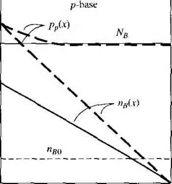 x = xb Figure 10.23 I Minority and inajority carrier concentrations in the base under low and high injection (solid line: low injection; dashed line: high injection). о jc: 0-00 10 7 = 300 К 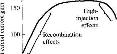 10 10 Collector current (Л) Figure 10.24 i Common-emitter current gain versus collector current. (From Shur/131) curve. The \ov gain at low currents is due to the small recombination factor and the drop-off at the high current is due to the high-injection effect. We will now consider the second high-injection effect. At low injection, the majority carrier hole concentration at jc - 0 for the npn transistor is Pp(0) = Ppo -and the minority carrier electron concentration is (10.46# (10. The pn product is (10. At high injection. Equation (10.46c) still applies. However, Ррф) will also increase, and for very high injection it will increase at nearly the same rate as Пр(0), The ia-crease in (0) will asymptotically approach the function /ОЧ /еУвЕ Прф)Проехр\р^ The excess minority carrier concentration in the base, and hence the collector current, will increase at a slower rate with B-E voltage in high injection than low injection. This effect is shown in Figure 10.25. The high-injection effect is very similar to the effect of a series resistance in a pn junction diode.  4> о 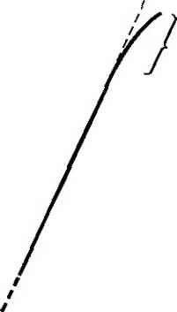 High-injection effects Ч Figure 10.25 1 Collector cnnenl versus base-emitter voltage showing high-injection effects. 10,4.3 Emitter Bandgap Narrowing Another phenomenon affecting the emitter injection efficiency is bandgap narrowing. We imphed from our previous discussion that the emitter injection efficiency factor would continue to increase and approach unity as the ratio of emitter doping to base doping continued to increase. As silicon becomes heavily doped, the discrete donor energy level in an n-type emitter splits into a band of energies. The distance between donor atoms decreases as the concentration of iinpurity donor atoms increases and the splitting of the donor level is caused by the interaction of donor atoms with each other. As the doping continues to increase, the donor band widens, becomes skewed, and moves up toward the conduction band, eventually merging with it. At this point, the effective bandgap energy has decreased. Figure 10.26 shows a plot of the change in the bandgap energy with impurity doping concentration. A reduction in the bandgap energy increases the intrinsic carrier concentration. The intrinsic carrier concentration is given by nj - N,.N exp (10.48) In a heavily doped emitter, the intrinsic carrier concentrarion can be written as nj = /Vf.A/ exp -(E,o-A£,0 kT nj exp (10.49) where Ego is the bandgap energy at a low doping concentration and AE is the bandgap narrowing factor. The emitter injection efficiency factor was given by Equation (10.35) as У = - РеоОеЕи tanh (хв/Ев) hboDbLe tanh (xe/Te) 1000 IT -о с с? cq
Figure 10.261 Bandgap-narrowing factor versus donor impurity concentration in silicon. (From Sze f 18].) The term /?eo is the thermal-equilibrium minority carrier concentration in the emitter and must be written as Ne Ne (1< As the emitter doping increases, AE increases; thus, po does not continue to crease with increased emitter doping. If peo starts to increase because of the bandgi narrowing, the emitter injection efficiency begins to fall off instead of continuing increase with increased emitter doping. EXAMPLE 10.7 Objective To determine the increase in p£o in the emitter due to bandgap narrowing. Consider a silicon emitter at Г = 300 К. Assume the emitter doping increases 10 cm to 10 cm~-. Calculate the change in the peo value. Solution For emitter dopings of Ne - lO cm~- and Ю'ст , we have, neglecting bandgap narrowing, Peo = nf (1.5 xlO) = 2.25 X 10- cm (1.5xl0 r 1 ;o = 1, - - 2.25 X 10 cm Taking into account the bandgap narrowing, we obtain, respectively, for = f 0* cm and Ne = 10 crr- PEi) (L5xny / 0.030 4 . ---7:tz--exp (----- 7.16 x 10 cm 10i V 0-0259 J Peo = (1.5 x 10 101 ) /01 \ - exp --- ) 1.07 X 10- cm- 0.0259/ Ш Comment If the emitter doping increases from 10 to 10 cm~-, the thermal-equilibrium minority carrier concentration actually increases by a factor of 1.5 instead of decreasing by the expected factor of 10. This effect is due to bandgap narrowing. As the emitter doping increases, the bandgap narrowing factor, AE will increase; this can actually cause Peo to increase. As peu increases, the emitter injecfion i efficiency decreases; this then causes the transistor gain to decrease, as in Figure 10.24. I A very high emitter doping may result in a smaller current gain than we anticipate because of the bandgap-narrowing effect. 10.4.4 Current Crowding It is tempting to minimize the effects of base current in a transistor since the base current is usually much smaller than either the collector or the emitter current. Figure 10.27 is a cross section of an npn transistor showing the lateral distribution of base current. The base region is typically less than a micrometer thick, so there can be a sizable base resistance. The nonzero base resistance results in a lateral potential difference under the emitter region. For the npn transistor, the potential decreases from the edge of the emitter toward the center. The emitter is highly doped, so as a first approximation the emitter can be considered an equipotential region. The number of electrons from the emitter injected into the base is exponentially dependent on the B-E voltage. With the lateral voltage drop in the base between the edge and center of the emitter, more electrons will be injected near the emitter edges than in the center, causing the emitter current to be crowded toward the edges. This current-crowding effect is schematically shown in Figure 10.28. The larger current density near the enutter edge may cause localized heating effects as well as localized high-injection effects. The nonuniform emitter current also results in a nonuniform lateral base current under the emitter. A two-dimensional analysis would be required to calculate the actual potential drop versus distance because of the nonuniform base current. Another approach is to slice the transistor into a number of smaller parallel transistors and to lump the resistance of each base section into an equivalent external resistance. Power transistors, designed to handle large currents, require large emitter areas to maintain reasonable current densities. To avoid the current-crowding effect, these transistors are usually designed with narrow emitter widths and fabricated with an in-terdigitated design. Figure 10.29 shows the basic geometry. In effect, many narrow emitters are connected in parallel to achieve the required emitter area. Base Emitter
Collector 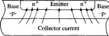 Figure 10.27 I Cross section of an npn bipolar transistor showing the base current distribution and the lateral potential drop in the base region. Figure 10.28 I Cross section of an npn bipolar transistor showing the emitter current-crowding effect. 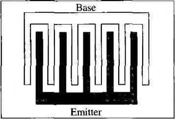  / Base / terminal Emitter terminal О 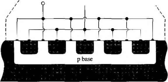 Figure 10.29 ! (a) Top view and (b) cross section of an jnterdigitated npn bipolar transistor structure. TEST YOUR UNDERSTANDING E 10.12 Consider the geometry shown in Eigure 10.30. The base doping concentration is V = 10 cm *, the neutral base width is д' = 0.80 дт, the emitter width is S = 10 дт, and the emitter length is L = 10 дт. (a) Determine the resistance of the base between jr = 0 and x = S/2. Assume a hole mobility of д^, = 400 cm/V-s. (h) If the base current in this region is uniform and given by /в/2 = 5 дА, determine the potential difference between x = 0 and x = S/2. (c) Using the results of part (b\ what is the ratio of emitter current density at x = 0 to that atx = S/2? [69 P) AUi g8 8l7 (Ф LL6 () *suv] * 10,4.5 Nonuniform Base Doping In the analysis of the bipolar transistor, we assumed uniformly doped regions. However, uniform doping rarely occurs. Figure 10.31 shows a doping profile in a doubly diffused npn transistor. We can start with a uniformly doped n-type substrate, diffuse acceptor atoms from the surface to form a compensated p-type base, and then diffuse donor atoms from the surface to form a doubly compensated n-type emitter, diffusion process results in a nonuniform doping profile. п collector Figure 10.30 I Figure for El0.12. 5 X 10 N 5 X JO* n-type emitter
\ N, p-tvpe 5 X 10 к \ base n-yP \ } collector Fijure 10.31 I Impurity concentration profiles of a double-diffused npn bipolar transistor. We determined in Chapter 5 that a graded impurity concentration leads to an induced electric field. For the p-type base region in thermal equilibrium, we can write Jp - eiXpNaE - eD (10.51) Then кГ\ 1 dN e ) Na dx (10.52) According to the example of Figure 10.31, dNa/dx is negative; hence, the induced electric field is in the negative x direction. Electrons are injected from the n-type emitter into the base and the minority carrier base electrons begin diffusing toward the collector region. The induced electric field in the base, because of the nonuniform doping, produces a force on the electrons in the direction toward the collector. The induced electric field, then, aids the flow of minority carriers across the base region. This electric field is called an accelerating field. The accelerating field will produce a drift component of current that is in tion to the existing diffusion current. Since the minority carrier electron concent tion varies across the base, the drift current density will not be constant. The t( current across the base, however, is nearly constant. The induced electric field in base due to nonunifonn base doping will alter the minority carrier distributii through the base so that the sum of drift current and diffusion current will be a stant. Calculations have shown that the uniformly doped base theory is very useful, for estimating the base characteristics. 10.4,6 Breakdown Voltage There are two breakdown mechanisms to consider in a bipolar transistor. The first called punch-through. As the reverse-bias B-C voltage increases, the B-C space charge region widens and extends farther into the neutral base. It is possible for the B-C depletion region to penetrate completely through the base and reach the B-E space charge region, the effect called punch-through. Figure 1032a shows the energy-band diagram of an npn bipolar transistor in thermal equilibrium and Figure 10.32h shows the energy-band diagram for two values of reverse-bias B-C junction voltage When a small C-B voltage, V/?], is applied, the B-E potential barrier is not affecle( thus, the transistor current is still essentially zero. When a large reverse-bias voltage Vr2, is applied, the depletion region extends through the base region and the B-potential barrier is lowered because of the C-B vohage. The lowering of the potentia barrier at the B-E junction produces a large increase in current with a very smal increase in C-B voltage. This effect is the punch-through breakdown phenomenon. Figure 10.33 shows the geometry for calculating the punch-through voltage. As sume that Nn and Nc are the uniform impurity doping concentrations in the base аш collector, respectively. Let 1Уд be the metallurgical width of the base and let jc be space charge width extending into the base from the B-C junction. If we neglect в в у V 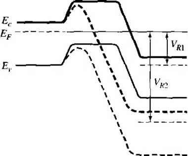 Figure 10.32 f Energy-band diagram of an npn bipolar transistor (a) in thermal equilibrium and (b) with a reverse-bias B-C voltage before punch-through, Vh\ and after punch-through, 1 2-
Figure 10.33 I Geometry of a bipolar transistor to calculate the punch-through voltage. narrow space charge width of a zero-biased or forward-biased B-E junction, then punch-through, assuming the abrupt junction approximation, occurs when - . We can write that 2eAVbi±Vp) Nc 1 Nb Nc + Nb (10.53) where Vpt is the reverse-biased B-C voltage at punch-through. Neglecring V/ compared to Vpr, we can solve for Vpt as eWl Nb{NcNb) (10.54) Objecrive To design the collector doping and collector width to meet a punch-through voltage specification. Consider a uniformly doped silicon bipolar transistor with a metallurgical base width of 0.5 дт and a base doping of Nb - 10 cm -\ The punch-through voltage is to be V =25V. Solution The maximum collector doping concentration can be determined from Equation (10.54) as (1.6 x 10 i)(0.5 x 10-*)(J0)(7Vr + 10*) 2(1E7)(8.85 X 10-)/Vc 12.94 = 1 -h с which yields Nc - 8.38 x 10 cm This n-type doping concentration in the collector must extend at least as far as the depletion width extends into the collector lo avoid breakdown in the collector region. We have, using design example 10.8  1 ... 38 39 40 41 42 43 44 ... 55 |
||||||||||||||||||||||||||||||||||||||||||||||||||||||
|
© 2026 AutoElektrix.ru
Частичное копирование материалов разрешено при условии активной ссылки |