 |
 |
 |
| Главная Журналы Популярное Audi - почему их так назвали? Как появилась марка Bmw? Откуда появился Lexus? Достижения и устремления Mercedes-Benz Первые модели Chevrolet Электромобиль Nissan Leaf |
Главная » Журналы » Absorbing materialorganic polymer 1 ... 39 40 41 42 43 44 45 ... 55 results from Chapter 1, x = в Neglecting Vbj compared to Vf - V, we obtain 2(И.7)(8.85 X lO-)(25) / 10 \ 1.6 x 10⁻¹ 8,38 X 10⁴ 10**+8.38 X 10* у 1/2 X = 5.97 pm Ш Comment From Figure 8.25, the expected avalanche breakdown voltage for this junction is greater 300 volts. Obviously punch-through will occur before the normal breakdown voltage in case. For a larger punch-through voltage, a larger metallurgical base width will be requij since a lower collector doping concentration is becoming impractical. A larger punch-through] voltage will also require a larger collector width in order to avoid premature breakdown in this] region. TEST YOUR UNDERSTANDING Е10ЛЗ The metallurgical base width of a silicon npn bipolar transistor is Wb = 0.80 m. The base and collector doping concentrations are IVв =2 x 10* cm- and Nc = 10 cm~\ Find the punch-through breakdown voltage. (A 803 suy) El O.I 4 The base impurity doping concentration is Nb =3 x 10* cm~ and the metallurgical base width is 0.70 /xm. The minimum required punch-through breakdown voltage is specified to be Vpi ~ 70 V. What is the maximum allowed collector doping concentration? i с[ОГ > 18 N suy) The second breakdown mechanism to consider is avalanche breakdown, but taking into account the gain of the transistor. Figure 10.34a is an npn transistor with a reverse-bias voltage applied to the B-C junction and with the emitter left open. The current IcBo is the reverse-biased junction current. Figure 10.34b shows the transistor with an applied C-E voltage and with the base terminal left open. This bias condition also makes the B-C junction reverse biased. The current in the transistor for this bias configuration is denoted as I ceo The current Icbo shown in Figure 10.34b is the normal reverse-biased B-C junction current. Part of this current is due to the flow of minority carrier holes from the collector across the B-C space charge region into the base. The flow of holes into the *Thc doping concentrations in the base and collector of the transistor we assume to be small enough that Zener breakdown is not a factor to be considered. 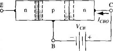 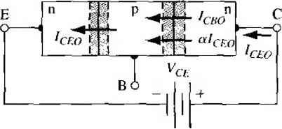 Figure 10.34 I (a) Open emiuer configuration with saturation current Icbo- (h) Open base configuration with saturation current Ictv- base niakes the base positive with respect to the emitter, and the B-E junction becomes forward biased. The forward-biased B-E junction produces the current Ico due primarily to the injection of electrons from the emitter into the base. The injected electrons diffuse across the base toward the B-C junction. These electrons are subject to all of the recombination processes in the bipolar transistor. When the electrons reach the B-C junction, this current component is a I ceo where a is the common base cunent sain. We therefore have ceo = ceo + cbo iced ~-- Pcbo ] -a (10.55a) (10.55b) where j6 is the common-emitter current gain. The reverse-biased junction current IcHo is multiplied by the current gain p when the transistor is biased in the open-base configuration. When the transistor is biased in the open-emitter configuration as in Figure 10.34a, the current Icbo t breakdown becomes Icso сво, where M is the multiplication factor. An empirical approximation for the multiplication factor is usually written as \-{VcbIBVcboY (10.56) where n is an empirical constant, usually between 3 and 6, and В Vcbo is the B-C breakdown voltage with the emitter left open. When the transistor is biased with the base open circuited as shown in Figure 10.34b, the currents in the B-C junction at breakdown are multiplied, so that IcEO - M {a I ceo + кво) (10.57) Solving for I ceo . we obtain CEO - 1 -аМ (10.58) The condition for breakdown corresponds to аМ = 1 00-59) Open base Open emitter Figure 10.351 Relative breakdown voltages and saturation currents of the open base and open emitter configurations. Using Equation (10.56) and assuming that Vca ce. Equation (10.59) becomes \-{BVcEolBVcmY where В Vceo is the C-E voltage at breakdown in the open base configuration. Solving for BVceo we find В Vceo = В VcboV 1 - or where, again, a is the common-base current gain. The common-emitter anil common-base current gains are related by I -ff (lO.K Normally a I, so that l- .i (10.6; Then Equation (10,61) can be written as В Vceo = (10.6; The breakdown voltage in the open-base configuration is smaller, by the factor than the actual avalanche junction breakdown voltage. This characteristic is shown it Figure 10.35. DESIGN EXAMPLE 10.9  Objective To design a bipolar transistor to meet a breakdown voltage specification. Consider a silicon bipolar transistor with a common-emitter current gain of j0 = 100 and a base doping concentration of Л^в = 10 cm~. The minimum open-base breakdown voltage, is to be 15 volts. I Solution From Equation (10.63), the minimum open-emitter junction breakdown voltage must be В Vcbo = у/Р^Усео Assuming the empirical constant n is 3, we find BVcBo = vT06(15) = 69.6 V From Figure 8.25, the maximum collector doping concentrarion should be approximately 7 x 10 cm~- to achieve this breakdown voltage. Comment In a transistor circuit, the transistor must be designed to operate under a worst-case situafion. In this example, the transistor must be able to operate in an open-base configuration without going into breakdown. As we determined previously, an increase in breakdown voltage can be achieved by decreasing the collector doping concentration. TEST YOUR UNDERSTANDING Е10Л5 A uniformly doped silicon transistor has base and collector doping concentrations of 5 X 10 cm~ and 5 x lO cm~-, respectively. The common emitter current gain is = 85. Assuming an empirical constant value of /7 = 3, determine BVceo-(A 9*13-suy) ElO.l6 The minimum required breakdown voltage of a uniformly doped silicon npn bipolar transistor is to be BVcto = 70 V. The base impurity doping concentration isiV = 3x 10cm~,the common-emitter current gain is = 85, and the empirical constant value is n = 3. Determine the maximum collector impurity doping concentrafion. (t-o oi \ N V) 10.5 I EQUIVALENT CIRCUIT MODELS In order to analyze a transistor circuit either by hand calculations or using computer codes, one needs a mathematical model, or equivalent circuit, of the transistor. There are several possible models, each one having certain advantages and disadvantages. A detailed study of all possible models is beyond the scope of this text. However, we will consider three equivalent circuit models. Each of these follows direcdy from the work we have done on the pn juncrion diode and on the bipolar transistor. Computer analysis of electronic circuits is more commonly used than hand calcularions, but it is instructive to consider the types of transistor model used in computer codes. It is useful to divide bipolar transistors into two categories-switching and amplification-defined by their use in electronic circuits. Switching usually involves turning a transistor from its off state, or cutoff, to its on state, either forward-active or saturation, and then back to its off state. Amplification usually involves superimposing sinusoidal signals on dc values so that bias voltages and currents are only perturbed. The Ebers-Moll model is used in switching applications; the hybrid-pi model is used in amplification applications. *10.5,1 Ebers-Moll Model The Ebers-Moll model, or equivalent circuit, is one of the classic models of the h lar transistor This particular model is based on the interacting diode junctions and applicable in any of the transistor operating tnodes. Figure 10.36 shows the current directions and voltage polarities used in the Ebers-Moll modeL The currents are fined as all entering the terminals so that  !e + h + IcO (10.( The direction of the emitter current is opposite to what we have considered up to point, but as long as wc are consistent in the analysis, the defined direction does matter. The collector current can be written in general as (10.6 where a;r is the common base current gain in the forward-active mode. In this mode, Equation (10.65a) becomes Ic=aFlf -h Ics (10.65Ь; where the current Ics is the reverse-bias B-C junction current. The current /г is given by  h - Ies (10.66) If the B-C junction becomes forward biased, such as in saturation, then we can write the current ? as Ir - Ics (10.  Using Equations (10,66) and (10.67), the collector current from Equation (10.65a) can be written as Ic ~ <eIes еУвЕ кТ (10.68)  в Figure 10.36 I Current direction and voltage polarity definitions for the Ebers-Moll model.   Ir ~ cs ()-i В Figure 10.371 Basic Ebers-Moll equivalent circuit. We can also write the emitter current as (10.69) Ie - (XrIcs  (10.70) The current fs is the reverse-bias B-E juncrion current and Qr is the common base current gain for the inverse-acrive mode. Equations (10.68) and (10,70) are the classic Ebers-Moll equations. Figure 10.37 shows the equivalent circuit corresponding to Equations (10.68) and (10.70). The ctzrrent sources in the equivalent circuit represent current components that depend on voltages across other junctions. The Ebers-Moll model has four parameters: а^а^, Ies. and Ics However, only three parameters are independent. The reciprocity relationship slates that (10.71) Since the Ebers-Moll model is valid in each of the four operating modes, we can, for example, use the model for the transistor in saturation. In the saturation mode, both B-E and B-C juncrions are forward biased, so that V > 0 and Vbc > 0. The B-E voltage will be a known parameter since we will apply a voltage across this junction. The forward-biased B-C voltage is a result of driving the transistor into saturation and is the unknown to be determined from the Ebers-Moll equations. Normally in electronic circuit applications, the coUectormitter voltage at saturation is of interest. We can define the C-E saturation voltage as Vce (sat) Vre- bc (10.72) We will find an expression for Vce (sat) by combining the Ebers-Moll equations. In the following example we see how the Ebers-Moll equations can be used in a hand calculation, and we may also see how a computer analysis would make the calculations easier. Combining Equations (10.64) and (10.70), we have -if в + /с) =CiRlcS If we solve for [exp (e Vnc/kT) - 1 ] from Equation (10.73), and substitute the rc ing expression into Equation (10.68), we can then find Vbe as V,\n /c(l - Qfj?) + /fl + Ies( - (Xer) (1074) where Vj is the thermal voltage. Similarly, if we solve for {eVв e I T) - 11 finm Equation (10.68), and substitute this expression into Equation (10.73), we can Vbc as V,\n gceIb - ( -а^)/с- + /cs(l -CiEOtR) fcsi -OtEOiR) (10.75) We may neglect the Ies and Ics terms in the numerators of Equations (10.74) and (10-75). Solving for Vc£(sat), we have Vc£(sat) = Vbe - Vcb = К In Ic(\ - aR) + Ib Ics ---rw --- ctflB - (1 -ar)Ic Ies. (10.76) The ratio of Ics to Ies ean be written in terms of af and aR from Equation (10.71), We can finally write Vc£(sat) - V, In /c-(l -ав) + /д Or аЕ1в - (1 -aг)c (1077) EXAMPLE ЮЛО Objective To calculate the coUeclor-emitter saturation vohage of a bipolar transistor al T = 300 K. Assume that ay = 0.99, ff/? = 0.20, Ic = I mA, and = 50 fiA. Solution Substituting the parameters into Equation (10.77) we have Vc£(sat)-3 (0.0259) In (l)(l -0.2) + (0.05) (0.99)(0.05) - (I -0.99)(I ) V0.20j 0121 V CoHfiment This VcE (sat) value is typical of collector-emitter saturation voltages. Because of the log function, VcE (sat) is not a strong function of I с or /д. 10.5-2 Gummel-Poon Model The Gummel-Poon model of the BJT considers more physics of the transistor than the Ebers-Moll model. This model can be used if, for example, there is a nonunifonn doping concentration in the base. The electron current density in the base of an npn transistor can be written as J,ciiMx)E-heD,- (10.78) electric field will occur in the base if nonuniform doping exists in the base. This was discussed in Section 10.4.5. The electric field, from Equarion (10.52), can be written in the form kT 1 dpix) E=---(10.79) e p(x) dx where p(x) is the majority carrier hole concentration in the base. Under low injection, the hole concentration is just the acceptor impurity concentration. With the doping profile shown in Figure 10.31, the electric field is negarive (from the collector to the emitter). The direction of this electric field aids the flow of electrons across the base. Substituting Equarion (10.79) into Equation (10.78), we obtain kT 1 dpix) dn{x) Jn = epMx)------4 + eDt, - (10.80) В e p(x) dx dx Using Einsteins relarion, we can write Equation (10.80) in the form еД, / dp{x) dn[x)\ eD d{pn) oi4 Л - -- - + p{x)-.- - -- --- (10.81) p{x) \ dx dx ) p(x) dx , Equation (10.81) can be written in the form JnP(x) d(pri) eDfj dx (10.82) Integrating Equation (10.82) through the base region while assuming that the electron current density is essentially a constant and the diffusion coefficient is a constant, we find / p{x)dx - / dx = р{хв)п(хв) - p(0)n(0) (10.83) f Д| Jo Jo dx Assuming the B-E junction is forward biased and the B-C junction is reverse biased, we have n(0) = пво exp {Уве/У^ and п{хв) - 0. We may note that пвоР = so that Equation (10.83) can be written as p{x)dx The integral in the denominator is the total majority carrier charge in the base and is known as the base Gummel number, defined as Qb- If we perform the same analysis in the emitter, we find that the hole current density in the emitter of an npn transistor can be expressed as -еРрп]хр{УвЕ1Уд n{x) dx  The integral in the denominator is the total majority carrier charge in the emitter and is known as the emitter Gummel number, defined as . Since the currents in the Gummel-Poon model are functions of the total inte grated charges in the base and emitter, these currents can easily be determined fof nonuniformly doped transistors. The Gummel-Poon model can also take into account nonideal effects, such the Early effect and high-level injection. As the B-C voltage changes, the neu base width changes so that the base Gummel number Qe changes. The change in Q with B-C voltage then makes the electron current density given by Equation (10,84) a function of the B-C voltage. This is the base width modulation effect or Early effect as discussed previously in Section 10.4.1. If the B-E voltage becomes loo large, low injection no longer applies, which leads to high-level injection. In this case, the total hole concentration in the base increases because of the increased excess hole concentration. This means that the base Gummel number will increase. The change in base Gummel number implies, from Equation (10.84), that the electron current density will also change. High-level injection was also previously discussed in Section 10.4.2. The Gummel-Poon model can then be used to describe the basic operation of the transistor as well as to describe nonideal effects. 10,53 Hybrid-Pi Model Bipolar transistors are commonly used in circuits that amplify time-varying or sinusoidal signals. In these linear amplifier circuits, the transistor is biased in the forward-active region and small sinusoidal voltages and cunents are superimposed on dc voltages and currents. In these applications, the sinusoidal parameters are of interest, so it is convenient to develop a small-signal equivalent circuit of the bipolar transistor using the small-signal admittance parameters of the pn junction developed in Chapter 8, Figure 10-38a shows an npn bipolar transistor in a common emitter configuration with the small-signal terminal voltages and currents. Figure 10.38b shows the cross section of the npn transistor. The C, B, and E terminals are the external connections to the transistor, while the С, B, and E points are the idealized intemal coU lector, base, and emitter regions. We can begin constructing the equivalent circuit of the transistor by considering the various terminals individually. Figure 10.39a shows the equivalent circuit between the external input base terminal and the external emitter terminal. The resistance is the series resistance in the base between the external base terminal В and the internal base region The B-E junction is forward biased, so is the junction diffusion capacitance and is the junction diffusion resistance. The diffusion capacitance Cj is the same as the diffusion capacitance Cj given by Equation (8.72), and the diffusion resistance is the same as the diffusion resistance given by Equation (8.35). The values of both parameters are functions of the junction current. These two elements are in parallel with the junction capacitance, which is Cj. Finally, ,v is the series resistance between the external emitter terminal and the 4> О E (a) 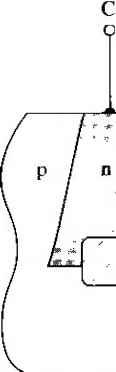 В О В с о
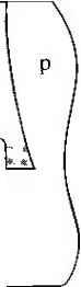 Figure 10.38 1 (a) Common emitter npn bipolar transistor with small-signal current and voltages, (b) Cross sectit)n of an npn bipolar transistor for the hybrid-pi model. 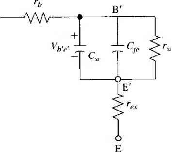 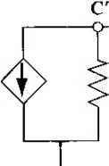 B СУ- Figure 10.39 I Components of the hybrid-pi equivalent circuit between (a) the base and emitter, (b) the collector and emitter, and (c) the base and collector. 1 ... 39 40 41 42 43 44 45 ... 55 |
|
© 2026 AutoElektrix.ru
Частичное копирование материалов разрешено при условии активной ссылки |