 |
 |
 |
| Главная Журналы Популярное Audi - почему их так назвали? Как появилась марка Bmw? Откуда появился Lexus? Достижения и устремления Mercedes-Benz Первые модели Chevrolet Электромобиль Nissan Leaf |
Главная » Журналы » Absorbing materialorganic polymer 1 ... 40 41 42 43 44 45 46 ... 55 гЛ/vV E О 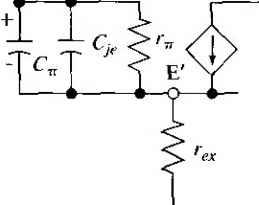 Figure 10.401 Hybrid-pi equivalent circuit. intemal emitter region. This resistance is usually very small and may be on the or of 1 to 2 Q. Figure ] 0.39b shows the equivalent circuit looking into the collector terminal The Гс resistance is the series resistance between the external and intemal collectof connections and the capacitance C, is the junction capacitance of the reverse-biased collector-substrate junction. The dependent current source, gmbt is the collector current in the transistor, which is controlled by the intemal base-emitter voltage. The resistance is the inverse of the output conductance go and is primarily due to the Early effect. Finally, Figure 10.39c shows the equivalent circuit of the reverse-biased B-C juncrion. The parameter is the reverse-biased junction capacitance and is the reverse-biased diffusion resistance. Normally, is on the order of megohms and can be neglected. The value of is usually much smaller than C-r but, because of the feedback effect which leads to the Miller effect and Miller capacitance, cannot be ignored in most cases. The Miller capacitance is the equivalent capacitance between B and E due to C and the feedback effect, which includes the gain of the transisior. The Miller effect also reflects C between the С and E terminals at the output. However, the effect on the output characteristics can usually be ignored. Figure 10.40 shows the complete hybrid-pi equivalent circuit. A computer sim-ularion is usually required for this complete model because of the large number of elements. However, some simplifications can be made in order to gain an appreciation for the frequency effects of the bipolar transistor. The capacitances lead to frequency efiects in the transistor, which means that the gain, for example, is a function of the input signal frequency. Objective To determine, to a first approximation, the frequency at which the small-signal current gain decreases to I/л/2 of its low frequency value. с  Figure 10.41 i Simplified hybrid-pi equivalent circuit Consider the simplified hybrid-pi circuit shown in Figure 10.41. We are ignoring C,, Cs, fxy Cje, ro, and the series resistances. We must emphasize that this is a first order calculation and that Cfj, normally cannot be neglected. Solution At very low frequency, we may neglect C so that Vhe = and = Vbe = gm rjt h We can then write where his the low-frequency, small-signal common emitter current gain. Taking into account C, we have Vbe = h Then h = gm Vbe - Ib 1 +ja)rC, or the small-signal current gain can be written as The magnitude of the current gain drops to 1/л/2 of its low-frequency value at / If, for example, =2.6 kQ and C = 4 pF, then / = 15.3 MHz Comment High-frequency transistors must have small diffusion capacitances, implying the use of small devices. CHAPTER 10 The Bi polar Transistor 10.6 I FREQUENCY LIMITATIONS The hybrid-pi equivalent circuit, developed in the last section, introduces frequency fects through the capacitor-resistor circuits. We will now discuss the various physic factors in the bipolar transistor affecting the frequency limitations of the device, then define the transistor cutoff frequency, which is a figure of merit for a transistor. 10.6.1 Time-DeJay Factors The bipolar transistor is a transit-time device. When the voltage across the B-E junc] tion increases, for example, additional carriers from the emitter are injected into base, diffuse across the base, and are collected in the collector region. As the fre- quency increases, this transit time can become comparable to the period of the input signal. At this point, the output response will no longer be in phase with the input the magnitude of the current gain will decrease. The total emitter-to-collector time constant or delay time is composed of fc separate time constants. We can write Tcr ~ te + + td + Tt ITO.86] where emitier-to-coUector time delay - emitter-base junction capacitance charging time т/, - base transit time Id = collector depletion region transit time r,. = collector capacitance charging time The equivalent circuit of the forward-biased B-E junction was given in Fig-j ure 10.39a. The capacitance Cj is the junction capacitance. If we ignore the seri( resistance, then the emitter-base junction capacitance charging time is (Ш.87Г where is the emitter junction or diffusion resistance. The capacitance Cp includes any parasitic capacitance between the base and emitter. The resistance г/, is found as the inverse of the slope of the versus Vbf: curve. We obtain kT 1 (10.88) where Ie is the dc emitter current. The second term, гь. is the base transit time, the time required for the minority carriers to diffuse across the neutral base region. The base transit time is related to the diffusion capacitance C: of the B-E junction. For the npn transistor, the electron current density in the base can be written as Л = -епв{х)у{х) (10,89) 10-6 Frequency Lim itations where v{x) is an average velocity. We can write Ф v{x) = dx/dt or dtdx/v{x) The transit time can then be found by integrating, or (10.90) h Jo Jo (-Jn (10.91) The electron concentration in the base is approximately linear (see Example 10.6) so we can write Пв{х) ПВО (10.92) and the electron current density is given by Jn = eDrr dHBJx) dx (10.93) The base transit time is then found by combining Equations (10.92) and (10.93) with Equation (10.91). We find that (10.94) The third time-delay factor is r, the collector depletion region transit time. Assuming that the electrons in the npn device travel across the B-C space charge region at their saturation velocity, we have   (10.95) where x. is the B-C space charge width and l\ is the electron saturation velocity. The fourth time-delay factor, r., is the collector capacitance charging time. The B-C is reverse biased so that the diffusion resistance in parallel with the junction capacitance is very large. The charging time constant is then a function of the collector series resistance r. We can write (10.96) where Cf is the B-C junction capacitance and Q is the collector-to-substrate capacitance. The series resistance in small epitaxial transistors is usually small; thus the time delay r, may be neglected in some cases. Example calculations of the various time-delay factors will be given in the next section as part of the cutoff frequency discussion. 10-6.2 Transistor Cutoff Frequency The current gain as a function of frequency was developed in Example 10 Jl so tha: we can also write the common base current gain as (10.97: where ao is the low-frequency common base current gain and f, is defined as the alpha cutoff frequency. The frequency fa is related to the emitter-to-collector tim delay Tec as Л = (10.981 When the frequency is equal to the alpha cutoff frequency, the magnitude of the common base current gain is \/\/2of its low-frequency value. We can relate the alpha cutoff frequency to the common emitter current gain b\ considering I -a (lOi We may replace a in Equation (10.99) with the expression given by Equation (10. When the frequency / is of the same order of magnitude as then (10.11 where we have assumed that ao 1. When the signal frequency is equal to the alpha cutoff frequency, the magnitude of the common emitter current gain is equal to unity. The usual notation is to define this cutoff frequency as /V, so we have (lo.ioi; From the analysis in Example 10.11, we may also write the common-emitter current gain as 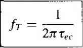 1+Л Л) (10.102) where f is called the beta cutoff frequency and is the frequency at which the magnitude of the common-emitter current gain drops to 1 /\f2 of its low-frequency value. Combining Equations (10.99) and (10.97), we can write i+jif/fr) l-ao + jif/fr) 10-6 Frequency Limitations where  Figure 10.42 I Bode plot of common emitter current gain versus frequency. (l-to)/7 .ft/ I - ao t - ofo (10.104) Comparing Equations (10.104) and (10.102), the beta cutoff frequency is related to the cutoff frequency by (10.105) 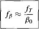 Figure 10.42 shows a Bode plot of the common emitter current gain as a function of frequency and shows the relative values of the beta and cutoff frequencies. Keep in mind that the frequency is plotted on a log scale, so and fr usually have significantly different values. Objective To calculate the emitter-to-collector transit time and the cutoff frequency of a bipolar transistor, given the transistor parameters. Consider a silicon npn transistor at T = 300 K. Assume the following parameters: Ie = 1 mA Cjt, - 1 pF Xb - 0.5 дт Д, = 25 cm/s jTrf,- = 2.4 л 20 C,=0.1pF C, =0.1pF EXAMPLE 10.12 Solution We will initially calculate the various time-delay factors. Tf we neglect the parasitic ca tance, the emitter-base junction charging time is where Then The base transit time is e Ie 1 X 10-3 = (25.9)(10-=) = 25.9 ps xl (0.5 X \0-y = 20; 2(25) =P The collector depletion region transit time is x 2.4 x The collector capacitance charging time is Гс = rACf, -h C,) = (20)(0.2 x 10--) = 4 ps The total emiUer-to-collector time delay is then T = 25.9 -b 50 + 24 + 4 = 103.9 ps so that the cutoff frequency is calculated as 2 = 2л(103.9х10-=) = - If wc assume a low-frequency common-emitter current gain of 100, then the beta cutoff frequency is fr 1.53 x 10 (в = - = -7:7.- 15.3 MHz 0 100 Comment The design of high-frequency transistors requires small device geometries in order to reduce capacitances, and narrow base widths in order to reduce the base transit time. TEST YOUR UNDERSTANDING Е10Л7 A silicon npn bipolar transistor is biased at /я =0.5 mA and has a junction capacitance of C,> = 2 pp. All other parameters are the same as listed in Example 10.12. Find the emitter-to-collector transit time, the cutoff frequency, and the beta cutoff frequency. iUn V\] = mO PVl = V sd9 181 = uy) ЮЛ I LARGE-SIGNAL SWITCHING Switching a transistor from one state to another is strongly related to the frequency characteristics just discussed. However, switching is considered to be a large-signal change whereas the frequency effects assumed only small changes in the inagnitude of the signal. 10.7Л Switching Characteristics Consider an npn transistor in the circuit shown in Figure 10.43a switching from cutoff to saturation, and then switching back from saturation to cutoff. We will describe the physical processes taking place in the transistor during the switching cycle. Consider, initially, the case of switching from cutoff to saturation. Assume that in cutoff VsE Vbb < 0, thus the B-E junction is reverse biased. At / =0, assume that Vbb switches to a value of Vbbo iis shown in Figure 10-43b. We will as.sume that Vo is sufficiently positive to eventually drive the transistor into saturation. For 0 < < f 1, the base current supplies charge to bring the B-E junction from reverse bias to a slight forward bias. The space charge width of the B-E junction is narrowing, and ionized donors and acceptors are being neutralized. A small amount of charge is also injected into the base during this time. The collector current increases from zero to 10 percent of its final value during this rime period, referred to as the delay rime. с BBi) Time t = 0 /c<saO 0.9 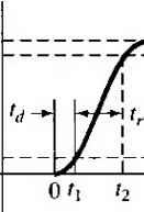 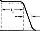 4 rime Figure 10.43 I (a) Circuit used for transistor switching, (b) Input base drive for transistor switching, (c) Collector current versus time during transistor switching. CHAPTER 10 TheBipolar Transistor During the next time period, t] <.t <t2. the base current is supplying ch which increases the B-E junction voltage from near cutoff to near saturation. Duri this time, additional carriers are being injected into the base so that the gradient of minority carrier electron concentration in the base increases, causing the colle current to increase. We refer to this time period as the rise time, during which the о lector current increases from 10 percent to 90 percent of the final value. For t > t\ the base drive continues to supply base current, driving the transistor into saturati and establishing the final minority carrier distriburion in the device. The switching of the transistor from saturation to cutoff involves removing all the excess minority carriers stored in the emitter, base, and collector regions. Fi ure 10.44 shows the charge storage in the base and collector when the transistor is saturation. The charge is the excess charge stored in a forward-acrive transist and Qbx and Qc are the extra charges stored when the transistor is biased in sat rion. At r - f-j, the base voltage Vbb switches to a negative value of (-V/f). The current in the transistor reverses direction as was the case in switching a pn juncti diode from forward to reverse bias. The reverse base current pulls the excess sto carriers from the emitter and base regions. Initially, the collector current does change significantly, since the gradient of the minority carrier concentration in the base does not change instantaneously. Recall that when the transistor is biased in sat-l urarion, both the B-E and B-C junctions are forward biased. The charge Qbx in the base must be removed to reduce the forward-biased B-C voltage to zero volts before the collector current can change. This time delay is called the storage time and is de- noted by fv The storage time is the time between the point at which Vbb switches tofl the time when the collector current is reduced to 90 percent of its maximum saturation value. The storage time is usually the most important parameter in the switching speed of the bipolar transistor. The final switching delay time is the fall time tj during which the collector current decreases from the 90 percent to the 10 percent value. During this time, the 641  Emitter Minority carrier concentration 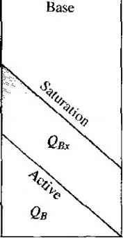 Collector 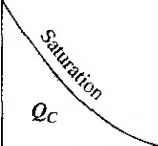 Figure 10.441 Charge storage in the base and collector at saturation and in the active mode. junction is reverse biased but excess carriers in the base are still being removed, and the B-E junction voltage is decreasing. The switching-time response of the transistor can be determined by using the Ebers-Moll model. The frequency-dependent gain parameters must be used, and normally the Laplace transform technique is used to obtain the time response. The details of this analysis are quite tedious and will not be presented here. 10.7.2 The Schottky-Clamped Transistor One method frequently employed to reduce the storage time and increase the switching speed is the use of a Schottky-clamped transistor. This is a normal npn bipolar device with a Schottky diode connected between base and collector, as shown in Figure 10.45a. The circuit symbol for the Schottky-clamped transistor is shown in Figure 10.45b. When the transistor is biased in the forward-active mode, the B-C junction is reverse biased; hence, the Schottky diode is reverse biased and effectively out of the circuit. The characteristics of the Schottky-clamped transistor-or simply the Schottky transistor-are those of the normal npn bipolar device. When the transistor is driven into saturation, the B-C junction becomes forward biased; hence the Schottky diode also becomes forward biased. We may recall from our discussion in the previous chapter that the effective turn-on voltage of the Schottky diode is approximately half that of the pn junction. The difference in turn-on voltage means that most of the excess base current will be shunted through the Schottky diode and away from the base so that the amount of excess stored charge in the base and collector is drastically reduced. The excess minority carrier concentration in the base and collector at the B-C junction is an exponential function of Vc. If V/c is reduced from 0.5 volt to 0.3 volt, for example, the excess minority carrier concentration is reduced by over 3 orders of magnitude. The reduced excess stored charge in the base of the Schottky transistor greatly reduces the storage time-storage times on the order of 1 ns or less are common in Schottky transistors. Б В Figure 10,45 I (a) The Schottky-clamped transistor (b) Circuit symbol of the Schottky-clamped transistor. 1 ... 40 41 42 43 44 45 46 ... 55 |
|
© 2026 AutoElektrix.ru
Частичное копирование материалов разрешено при условии активной ссылки |