 |
 |
 |
| Главная Журналы Популярное Audi - почему их так назвали? Как появилась марка Bmw? Откуда появился Lexus? Достижения и устремления Mercedes-Benz Первые модели Chevrolet Электромобиль Nissan Leaf |
Главная » Журналы » Absorbing materialorganic polymer 1 ... 41 42 43 44 45 46 47 ... 55 С н А Р т Е R 10 The Bipolar 1 ransistor *10.8 I OTHER BIPOLAR TRANSISTOR STRUCTURES This section is intended to briefly introduce three specialized bipolar transistor structures. The first structure is the polysilicon emitter bipolar juncrion transistor (BJT), the second is the SiGe-base transistor, and the third is the heterojunction bipolar transistor (HBT). The polysilicon emitter BJT is being used in some recent integrated circuits, and the SiGe-base transistor and HBT are intended for high-frequency/highspeed applications. 10,8,1 Polysilicon Emitter BJT The emitter injection efficiency is degraded by the carriers injected from the base back into the emitter. The emitter width, in general, is thin, which increases speed and reduces parasitic resistance. However, a thin emitter increases the gradient in the minority carrier concentration, as indicated in Figure 10.19. The increase in the gradient increases the B-E junction current, which in turn decreases the emitter injection efficiency and decreases the common emitter current gain. This effect is also shown in the summary of Table 10.3. Figure 10.46 shows the idealized cross section of an npn bipolar transistor with a polysilicon emitter. As shown in the figure, there is a very thin n single crystal silicon region between the p-type base and the n-type polysilicon. As a first approximation to the analysis, we may treat the polysilicon portion of the emitter as low-mobility silicon, which ineans that the corresponding diffusion coefficient is small. Assuming that the neutral widths of both the polysilicon and single-crystal portions of the emitter are much smaller than the respective diffusion lengths, then the minority carrier distribution functions will be linear in each region. Both the minonty carrier concentration and diffusion current must be continuous across the polysilicon/ silicon interface. We can therefore write (10Л< 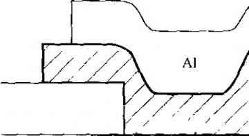 p base  n * polysilicon SiO, n coUc\;tor Figure 10.46 I Siinplified cross section of an npn polysilicon emitter BJT. Metal n poly emitter 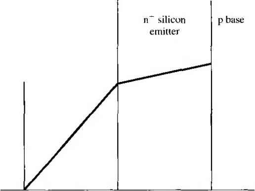 Figure 10,47 I Excess minority carrier hole concentrations in n polysilicon and n+ silicon emitter d{8pE(n-)) /Г(ро1у) d{8pE(po]y)) (ЮЛОбЬ) Since Д:(ро[>) < £*е(п+), then the gradient of the minority carrier concentration at the emitter edge of the B-E depletion region in the n+ region is reduced as Figure 10.47 shows. This implies that the current back-injected from the base into the emitter is reduced so that the common-emitter current gain is increased. 10.8.2 Silicon-Germanium Base Transistor ТЪе bandgap energy of Ge ( 0.67 eV) is significantly smaller than the bandgap energy of Si(1.12eV). By incorporating Ge into Si, the bandgap energy will decrease compared to pure Si. If Ge is incoфorated into the base region of a Si bipolar transistor, the decrease in bandgap energy will influence the device characterisfics. The desired Ge concentration proflle is to have the largest amount of Ge near the base-collector junction and the least amount of Ge near the base-emitter junction. Figure 10.48a shows an ideal uniform boron doping concentration in the p-type base and a linear Ge concentration profile. The energy bands of a SiOe-base npn transistor compared to a Si-base npn transistor, assuming the boron and Ge concentrations given in Figure 10.48a, are shown in Figure 10.48b. The emitter-base junctions of the two transistors are essentially idemical, since the Ge concentration is very small in this region. However, the bandgap energy of the SiGe-base transistor near the base 4;ollector junction is smaller than that of the Si-base transistor. The base current is determined by the base-emitter junction parameters and hence will be essentially the same in the two transistors. This change in bandgap energy will influence the collector current. Concentration Boron 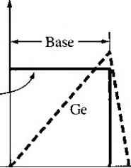 Base Si base 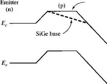 Collector (n) Figure 10.48 f (a) Assumed boron and germanium concentradons in the base of the SiGe-base transistor (b) Energy band diagram of the Si- and SiGe-base transistors. Collector Current and Current Gain Effects Figure 10.49 shows the therms equilibrium minority carrier electron concentration through the base region of SiGe and Si transistors. This concentration is given by (lO.li в where Nb is assumed to be constant. The intrinsic concentration, however, is a func- tion of the bandgap energy. We may write /7 (SiGe) (AE. = exp I nfiSi) (10.1081 where л,-(SiGe) is the intrinsic carrier concentration in the SiGe material, ,(Si) is the intrinsic carrier concentration in the Si material, and AE is the change in the bandgap energy of the SiGe material compared to that of Si. The collector current in a SiGe-base transistor will increase. As a first approximation, we can see this from the previous analysis. The collector current was found from Equation (10.36a), in which the derivative was evaluated at the base-collector Electron concentration Emitter Base no SiGc base  Collector Figure 10.49 I Thermal equiUbrium minority carrier electron concentration through the base of the Si- and SiGe-base transistors. junction. This means that the value of n in the collector current expression in Equation (10.37) is the value at the base-collector junction. Since this value is larger for the SiGe-base transistor (Figure 10.49), the collector current will be larger compared to the Si base transistor. Since the base currents are the same in the two transistors, the increase in collector current then implies that the current gain in the SiGe-base transistor is larger. If the bandgap narrowing is 100 meV, then the increase in the collector current and current gain will be approximately a factor of four. Early Voltage Effects The Early voltage in a SiGe-base transistor is larger than that of the Si-base transistor. The explanation for this effect is less obvious than the explanation for the increase in collector current and current gain. For a bandgap narrowing of 100 meV, the Early voltage is increased by approximately a factor of 12. Incorporating Ge into the base region can increase the Early voltage by a large factor. Base Transit Time and Emitter-Base Charging Time Effects The decrease in bandgap energy from the base-emitter junction to the base-collector junction induces an electric field in the base that helps accelerate electrons across the p-type base region. For a bandgap narrowing of 100 meV, the induced electric field can be on the order of 10 * to 10 * V/cm. This electric field reduces the base-transit time by approximately a factor of 2.5. The emitter-base junction charging fime constant, given by Equation (10.87), is directly proportional to the emitter diffusion resistance r. This parameter is inversely proportional to the emitter current, as seen in Equation (10.88). For a given base current, the emitter current in the SiGe-base transistor is larger, since the current gain is larger. The emitter-base junction charging time is then smaller in a SiGe-base transistor than that in a Si-base transistor. The reduction in both the base-transit fiine and the emitter-base charging time increases the cutoff frequency of the SiGe-base transistor. The cutoff frequency of these devices can be substantially higher than that of the Si-base device. 10.83 Heterojunction Bipolar Transistors As mentioned previously, one of the basic limitations of the current gain in the bipolar transistor is the emitter injection efficiency. The emitter injection efficiency у can be increased by reducing the value of the thermal-equilibrium minority carrier concentration Peq in the emitter. However, as the emitter doping increases, the bandg narrowing effect offsets any improvement in the emitter injection efficiency. 0 possible solution is to use a wide-bandgap material for the emitter, which will minimize the injection of carriers from the base back into the emitter. Figure 10.50a shows a discrete aluminum gallium arsenide/gallium arsenide het-! erojunction bipolar transistor, and Figure 10.50b shows the band diagram of the 1Ы Emitter J n GaAs n GaAlAs p GaAs n GaAIAs  Base nGaAs / X . п'СаАя / / Collector n+ GaAs 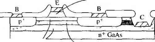 n GaAIAs p GaAs (a) т  ± Figure 10.50 I (а) Cross section of AlGaAs/GaAs heterojunction bipolar transistor showing a discrete and integrated structure, (b) Energy-band diagram of the n AlGaAs etnitter and p GaAs base junchon, {From Tiwari et ai {19].) 10-9 Summary 435 п-AlGaAs emitter to p-GaAs base junction. The hirge potential barrier V/, hmits the number of holes that wilt be injected back from the base into the emitter The intrinsic carrier concentration is a function of bandgap energy as nj ОС exp For a given emitter doping, the number of minority carrier holes injected into the i emiUer is redtjced by a factor of in changing from a narrow- to wide-bandgap emitter. If Д = 0.30 eV, for example, [ nf would be reduced by approximately 10 at 7 = 300 К. The drastic reduction mnj for the wide-bandgap emitter means that the requirements of a very high emitter doping can be relaxed and a high emitter injection efficiency can still be obtained. A lower emitter doping reduces the bandgap-narrowing effect. The heterojuncrion GaAs bipolar transistor has the potenrial of being a very high , frequency device. A lower emitter doping in the wide-bandgap emitter leads to a : smaller junction capacitance, increasing the speed of the device. Also, for the GaAs npn device, the minority carriers in the base arc electrons with a high mobility. The electron mobility in GaAs is approximately 5 times that in silicon; thus, the base transit time in the GaAs base is very short. Experimental AlGaAs/GaAs heterojunction transistors with base widths on the order of 0.1 m have shown cutoff frequencies on the order of 40 GHz. One disadvantage of GaAs is the low minority carrier liferime. The small lifetime is not a factor in the base of a narrow-base device, but results in a larger B-E recombination current, which decreases the recombination factor and reduces the current gain. A current gain of 150 has been reported. 10.9 I SUMMARY There are two complementary bipolar transistors-npn and pnp. Each transistor has three separately doped regions and two pn junctions. The center region (base) is very narrow, so the two pn junctions are said to be interacting junctions. In the forward-active mode, the B-E junction is forward biased and the B-C junction is reverse biased. Majority carriers from the emitter are injected into the base where they become minority carriers. These minority carriers diffuse across the base into the B-C space charge region where they are swept into the collector When a transistor is biased in the forward-active mode of operation, the current at one terminal of the transistor (collector current) is controlled by the voltage applied across the other two terminals of the transistor (base-emitter voltage). This is the basic transistor action The minority carrier concentrations were determined in each region of the transistor. The principal currents in the device are determined by the diffusion of these minority carriers. The common-base current gain, which leads to the common-emitter current gain, is a function of three factors-emitter injection efficiency, base transport factor, and recombination factor The emitter injection efficiency takes into account carriers fi the base that are injected back into the emitter, the base transport factor takes into account recombination in the base region, and the recombination factor takes into account carriers that recombine within the forward-biased B-E junction. Several nonideal effects were considered; 1. Base width modulation, or Eariy effect-the change in the neutral base width with a change in B-C voltage, producing a change in collector current with a change in B-C or C-E voltage. 2. High-injection effects that cause the collector current to increase at a slower rate with base-emitter voltagc. 3. Emitter bandgap narrowing that produces a smaller emitter injection efficiency because of a very large emitter region doping concentration, 4. Current crowding effects that produce a larger current density at the emitter edge than in the center of the emitter, 5. A nonuniform base doping concentration that induces an electric field in the base region, which aids the flow of minority carriers across the base. 6. Two breakdown voltage mechanisms-punch-through and avalanche. Three equivalent circuits or mathematical models of the transistor were considered. The Ebers-Moll model and equivalent circuit are applicable in any of the transistor operating modes. The Gummcl-Poon model is convenient to use when nonuniform doping exists in the transistor. The small-signal hybrid-pi model applies to transistors operating in the forward-active mode in linear amplifier circuits. The cutoff frequency of a transistor, a figure of merit for the transistor, is the frequency at which the magnitude of the common-emitter current gain becomes equal to unity. The frequency response is a function of the emitter-base junction capacitance charging time, the base transit time, the collector depletion region transit time, and the collector capacitance charging time. The switching characteristics are closely related to the frequency limitations although switching involves large changes in currents and voltages. An important parameter in switching is the charge storage time, which applies to a transistor switching from saturation to cutoff. GLOSSARY OF IMPORTANT TERMS alpha cutoff frequency The frequency at which the magnitude of the common base current is I /л/2 of its low-frequency value; also equal to the cutoff frequency. bandgap narrowing The reduction in the forbidden energy bandgap with high emitter doping concentration. base transit time The time that it takes a minority carrier to cross the neutral base region. base transport factor The factor in the common base current gain that accounts for recombination in the neutral base width. base width modulation The change in the neutral base width with C-E or C-B voltage. beta cutoff frequency The frequency at which the magnitude of the common emitter current gain is l/\/2 of its low frequency value. Checkpoint 437 collector capacitance charging time The time constant that describes the time required for the BC and collector-substrate space charge widths to change with a change in emitter cun-ent. collector depletion region transit time The time (hat it takes a carrier to be swept across the B-C space charge region. common-base current gain The ratio of collector current to emitter current. common-emitter current gain The ratio of collector current to base current. current crowding The nonuniform current density across the emi tter junction area created by a lateral voltage drop in the base region due to a finite base current and base resistance. cutoff The bias condition in which zero- or reverse-bias voltages are applied to both transistor junctions, resulting in zero transistor currents. cutoff frequency The frequency at which the magnitude of the common emitter current gain is unity. early effect Another term for base width modulation. early voltage The value of voltage (magnitude) at the intercept on the voltage axis obtained by extrapolating the /с versus Vce curves to zero current. emitter-base junction capacitance charging time The fime constant describing the fime for the B-E space charge width to change with a change in emitter current. emitter injection efficiency factor The factor in the common-base current gain that takes into account the injecuon of carriers from the base into the emitter forward active The bias condifion in which the B-E junction is forward biased and the B-C junction is reverse biased. inverse active The bras condition in which the B-E junction is reverse biased and the B-C juncfion is forward biased. output conductance The ratio of a differential change in collector current to the corresponding differenfial change in C-E voltage. CHECKPOINT After studying this chapter, the reader should have the ability to: Describe the basic operation of the transistor. Sketch the energy bands of the transistor in thermal equilibrium and when biased in the various operafing modes. Calculate, to a good first approximation, the collector current as a funcrion of base-emitter voltage. Sketch the minority carrier concentrations throughout the transistor under the various operating modes. Define the various diffusion and other current components in the transistor from the minority carrier distribution curves. Explain the physical mechanisms of the current gain limiting factors. Define the current-limiting factors from the current components in the transistor. Describe the physical mechanism of base width modulation and its effect on the current-voltage characterisfics of the transistor, Describe the voltage breakdown mechanisms in a bipolar transistor. Sketch the simplified small-signal hybrid-pi equivalent circuit of the transistor biased in the forward-active mode. Describe quahtatively the four time-delay or time-constant components in the frequent response of the bipolar transistor. REVIEW QUESTIONS 1. Describe the charge flow in an npn bipolar transistor biased in the forward-active mode. Is the current by drift or diffusion? 2. Define the common-emitter current gain and explain why, to a first approximation, the current gain is a constant. 3. Explain the conditions of the cutoff, saturafion, and inverse-active modes. 4. Sketch the minority carrier concentrations in a pnp bipolar transistor biased in the forward-active mode. 5. Define and describe the three limiting factors in the common-base current gain. 6. What is meant by base width modulation? What is another term used for this effect? 7. What is meant by high injection? 8. Expl ai n e mi tter curre nt crowd i ng. 9. Define Icbo and Icfm and explain why I ceo > Icbo - 10. Sketch a simplified hybrid-pi model for an npn bipolar transistor and explain when equivalent circuit is used. IE Describe the time-delay factors in the frequency limitation of the bipolar transistor. 12. What is the cutoff frequency of a bipolar transistor? 13. Describe ihe response of a bipolar transistor when it is switching between saturation and cutoff. PROBLEMS (Note: in the following problems, use the transistor geometry shown in Eigure 10.13. Assi T = 300 к unless otherwise stated,) Section 10 Л The Bipolar Transistor Action 10Л For a uniformly doped n pn bipolar transistor in thennal equilibrium, (a) sketch the energy-band diagram, (h) sketch the electric tield through the device, and (c) repeat parts (a) and {h) for the transistor biased in the forward-active region. 10.2 Consider a p n+p bipolar transistor, uniformly doped in each region. Sketch the energy-band diagram for the case when the transistor is {a) in thermal equilibrium, (b) biased in the forward-active mode, (c) biased in the inverse-active region, and (d) biased in cutoff with both the B-E and B-C junctions reverse biased. 10.3 The parameters in the base region of an npn bipolar transistor are D = 20cm-/s, Пво = 10 cm -, jc = 1 /zm,andA5£ = 10 cm*. (a) Comparing Equations (10.1) and (10.2), calculate the magnitude of /5. (b) Determine the collector current for (/) Vbe = 0.5 V, ( ) Vbe = 0.6 V, and (iii) Vbe = 0.7 V. 10.4 Assume the common-base current gain for the transistor described in Problem 10.3 is a = 0.9920. (a) What is the common-emitter current gain pi [Note that = a/( 1 - a).](h) Determine the emitter and base currents corresponding to the collector currents determined in Problem 10.3b. Problems 4Э9 10.5 (a) In a bipolar transistor biased in the forward-active region, the base current is in = 6.0 дА and the collector current is ic =510 дА. Determine a, and i. (Note that / £ = ic + is) Ф) Repeat part (a) if in = 50 дА and ic = 2.65 mA. 10.6 Assume that an npn bipolar transistor has a common-emitter current gain of p = 100. (a) Sketch the ideal cuirent-voltage characteristics (ic versus vcfJ, li(e those in Figure 10.9, as ig varies from zero to O.I mA in 0.01-шА increments. Let Vce vary over the range 0 < S Ю V. (b) Assuming Vcc = 10 V and = 1 kQ in the circuit in Figure 10.8, superimpose the load line on the transistor characteristics in part (я), (с) Plot, on the resulting graph, the value of ic and Vce corresponding to is = 0.05 mA. Ш Consider Equation f 10.7), Assume Vcc = Ю V, Rc = 2 кЙ, and Ve = 0,6 V, (a) Plot Vcb versus fc over the range 0 < /с 5 5 mA. (b) At what value of I с does Vc =0? Section 10.2 Minority Carrier Distribution 10.8 A uniformly doped silicon npn bipolar transistor is to be biased in the forward-active mode with the B-C junction reverse biased by 3 V. The metallurgical base width is 1.10 дт. The transistor dopings are Ne = 10 cm Ng = 10 cmr, and Nc 10 cm~ (a)For T = ЗСЮ К, calculate the B-E voltage at which the minority carrier electron concentration at л = 0 is 10 percent of the majority carrier hole concentration, (b) At this bias, determine the minority carrier hole concentration at x = 0. (c) Determine the neutral base width for this bias. 10.9 A silicon npn bipolar transistor is uniformly doped and biased in the forward-active region. The neutral base width is .Vg = 0.8 дт. The transistor doping concentrations are Л^;: = 5 X 10 cm-\ = 10 cm \ and Л^г 10 cm-\ (a) Calculate the values of pfa). во- nd pa). Ф) For Vbe = 0.625 V, determine at jc = 0 and Pe at jc = 0. (c) Sketch the minority carrier concentrations through the device and label each curve. 10.10 A uniformly doped silicon pnp transistor is biased in the forward-acrive mode. The doping concentrations ore Ne = 10** cm~-, Nb =5 x 10 cm, and Nc = 10 cm (fl) Calculate the values of no, pgo, and /?co- Ф) For Veb = 0.650 V, determine ps at .r =0 and at ,r = 0. (c) Sketch the minority carrier concentrations through the device and label each curve. 10.11 Consider the minority carrier electron concentration in the base of an npn bipolar transistor as given by Equation (10.15a). In this problem, we want to compare the gradient of the electron concentration evaluated at the B-C junction to that evaluated at the B-E junction. In particular, calculate the ratio of d{5n в)/dx at JC = jcb {od{5nB)/dx at jc = 0 for (a) xb/Lb =0.1, Ф)хв/Ев = 1.0, and (c) Xb/Lb = 10. 10.12 Derive the expressions for the coefficients given by Equations (10.14a) and (10.14b). *10.13 Derive the expression for the excess minority carrier hole concentration in the base region of a uniformly doped pnp bipolar transistor operating in the forward-active region. 10.14 The excess electron concentration in the base of an npn bipolar transistor is given by Equation (10.15a). The linear approximation is given by Equarion (10.15b). If SriBox) is the linear approximation given by Equation (10.15b) and 8пв(х) is the 1 ... 41 42 43 44 45 46 47 ... 55 |
||||||||||||
|
© 2026 AutoElektrix.ru
Частичное копирование материалов разрешено при условии активной ссылки |