 |
 |
 |
| Главная Журналы Популярное Audi - почему их так назвали? Как появилась марка Bmw? Откуда появился Lexus? Достижения и устремления Mercedes-Benz Первые модели Chevrolet Электромобиль Nissan Leaf |
Главная » Журналы » Absorbing materialorganic polymer 1 ... 43 44 45 46 47 48 49 ... 55 an inversion charge density at the semiconductor surface. The threshold voltage is defined as the applied gate voltage required to create the inversion layer charge and is one of the important parameters of the MOSFET. The various types of MOSFETs are examined and a qualitative discussion of the current-voltage characteristics is initially presented. A mathematical derivation Qf the current-voltage relation is then covered in detail. The frequency response and limitations of the MOSFET are also considered. Although we have not discussed fabrication processes in any detail in this text, there is an MOS technology that should be considered, since it directly influences the characteristics and properties of the MOS devices and circuits. We will consider the complementary MOS (CMOS) process. The discussion of this technology will be brief, but should provide a good base for further in-depth study. 11.1 I THE TWO-TERMINAL MOS STRUCTURE The heart of the MOSFET is the metal-oxide-semiconductor capacitor shown in Figure 11.1. The metal may be aluminum or some other type of metal, although in many cases, it is actually a high-conductivity polycrystalline silicon that has been deposited on the oxide; however, the term metal is usually still used. The parameter tj in the figure is the thickness of the oxide and tox is the permittivity of the oxide. 11ЛЛ Energy-Band Diagrams The physics of the MOS structure can be more easily explained with the aid of the simple parallel-plate capacitor. Figure 11,2a shows a parallel-plate capacitor with the top plate at a negative voltage with respect to the bottom plate. An insulator material separates the two plates. With this bias, a negative charge exists on the top plate, a positive charge exists on the bottom plate, and an electric field is induced between the two plates as shown. The capacitance per unit area for this geometry is (11Л) .V Semiconductor substrate Metal Insulator (oxide) О Figure 11.1 I The basic MOS capacitor structure. 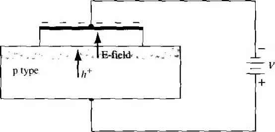 E field P type  Accumulation layer of holes Figure 11.2 I (a) A parallel-plate capacitor showing the electric field and conductor charges, (b) A corresponding MOS capacitor with a negafive gate bias showing the electric field and charge flow, (c) The MOS capacitor with an accumulafion layer of holes. where € is the permittivity of the insulator and d is the distance between the two plates. The magnitude of the charge per unit area on either plate is e-cv (11.2) where the prime indicates charge or capacitance per unit area. The magnitude of the electric field is Figure 11.2b shows an MOS capacitor with a p-type semiconductor substrate. The top metal gate is at a negative voltage with respect to the semiconductor substrate. From the example of the parallel-pi ate capacitor, we can see that a negative charge will exist on the top metal plate and an electric field will be induced with the direction shown in the figure. If the electric field were to penetrate into the semiconductor, the majority carrier holes would experience a force toward the oxide-semiconductor interface. Figure 11.2c shows the equilibrium distriburion of charge in the MOS capacitor with this particular applied voltage. An acciimidation layer of holes in the oxide-semiconductor juncrion corresponds to the positive charge on the bottom plate of the MOS capacitor. Figure 11.3a shows the same MOS capacitor in which the polarity of the appli( voltage is reversed. A positive charge now exists on the top metal plate and the ii duced electric field is in the opposite direction as shown. If the electric field pent trates the semiconductor in this case, majority carrier holes will experience a fore away from the oxide-semiconductor interface. As the holes are pushed away frot the interface, a negative space charge region is created because of the fixed ioni: acceptor atoms. The negative charge in the induced depletion region corresponds the negative charge on the bottom plate of the MOS capacitor. Figure 11.3b sho the equilibrium distribution of charge in the MOS capacitor with this applied voltaj The energy-band diagram of the MOS capacitor with the p-type substrate, for case when a negative voltage is applied to the top metal gate, is shown in Figure 11 j-The valence-band edge is closer to the Fermi level at the oxide-semiconductor interface than in the bulk material, which implies that there is an accumulation of hoU The semiconductor surface appears to be more p-type than the bulk material. Fermi level is a constant in the semiconductor since the MOS system is in thei equilibrium and there is no current through the oxide. Figure 11.4b shows the energy-band diagram of the MOS system when a tive voltage is applied to the gate. The conduction and valence band edges bend + + + + + + + + + + + + 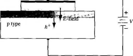 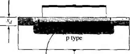 Induced space charge region Figure 11.3 I The MOS capacitor with a moderate positive gate bias, showing (a) the electric field and charge flow and (b) the induced space charge region. Gate Negative voltage applied -< Oxide  ptype Accumulation layer of holes (a) Gale Positive voltage applied 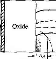 ptype Induced space charge region (b) Figure 11.41 The energy-band diagram of an MOS capacitor with a p-type substrate for (a) a negative gate bias and (b) a moderate positive gate bias. 11-1 The Two-Terminal MOS Structure hown in the figure, indicating a space charge region similar to that in a pn junction. The conduction band and intrinsic Fermi levels move closer to the Fermi level. The induced space charge width is x. Now consider the case when a still larger positive voltage is applied to the top metal gate of the MOS capacitor. We expect the induced electric field to increase in magnitude and the corresponding positive and negative charges on the MOS capacitor to increase. A larger negative charge in the MOS capacitor implies a larger induced space charge region and more band bending. Figure 11.5 shows such a condition. The intrinsic Fermi level at the surface is now below the Fermi level; thus, the conduction band is closer to the Fermi level than the valence band is. This result implies that the surface in the semiconductor adjacent to the oxide-semiconductor inteiiace is n type. By applying a sufficiently large positive gate voltage, we have inverted the surface of the semiconductor from a p-type to an n-type semiconductor. We have created an inversion tor of electrons at the oxide-semiconductor interface. In the MOS capacitor structure that we have just considered, we assumed a p-type semiconductor substrate. The same type of energy-band diagrams can be constructed for an MOS capacitor with an n-type semiconductor substrate. Figure 11.6a shows the MOS capacitor structure with a positive voltage applied to the top gate terminal. A positive charge exists on the top gate and an electric field is induced with the direction shown in the figure. An accumulation layer of electrons will be induced in Gate O- Large positive voltage  Inversion layer of electrons Oxide h  ptype Figure 11.5 I The energy-band diagram of the MOS capacitor with a p-type substrate for a large jx)sifive gate bias. + + + + + +  Accumulation layer of electrons  Induced positive space charge region Figure 11.61 The MOS capacitor with an n-type substrate for (a) a positive gate bias and (b) a moderate negative gate bias. the n-type substrate. The case when a negative vohage is applied to the top gate shown in Figure 11.6b. A positive space charge region is induced in the n-type seraij conductor in this situation. The energy-band diagrams for this MOS capacitor with the n-type substrate at shown in Figure 11.7. Figure 11.7a shows the case when a positive voltage is ap plied to the gate and an accumulation layer of electrons is formed. Figure 11.7 shows the positive space charge region induced by an applied negative gate voltage in it the conduction and valence band energies bend upward. Figure 11.7c shows th energy bands when a larger negative voltage is applied to the gate. The conduction and valence bands are bent even more and the intrinsic Fermi level has moved above the Fermi level so that the valence band is closer to the Fermi level than the Gate Positive voltage applied 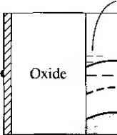 Accumulation of electrons n type Induced positive space charge region voltage applied 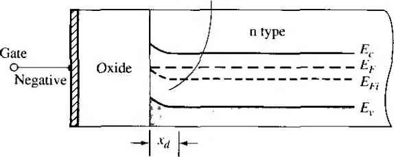 Gate Large-negative voltage 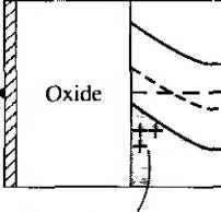 n type Inveriion layer of holes E. E - E, rw E. Figure 11.7 1 The energy-band diagram of the MOS capacitor with an n-type substrate for (a) a positive gate bias, (b) a mtxierate negative bias, and (c) a *large negative gate bias. conduction band is. This result implies that the semiconductor surface adjacent to the oxide-semiconductor interlace is p type. By applying a sufficiently large nega-[ tive voltage to the gate of the MOS capacitor, the semiconductor surface has been inverted from n type to p type. An inversion layer of holes has been induced at the oxide-semiconductor interface. 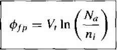 11 .L2 Depletion Layer Thickness We may calculate the width of the induced space charge region adjacent to the oxide-semiconductor interface. Figure 11.8 shows the space charge region in a p-type semiconductor substrate. The potential 0fpis the difference (in volts) between Epi and£,-and is given by (11-4) ; where is the acceptor doping concentration and /i, is the intrinsic carrier concentration. The potential is called the surface potential; it is the difference (in volts) between Efi measured in the bulk semiconductor and Ep{ measured at the surface. The surface potential is the potential difference across the space charge layer. The space charge width can now be written in a form similar to that of a one-sided pn junction. We can write that xd ( -i (П.5) where is the permittivity of the semiconductor. Equation (U.5) assumes that the abrupt depletion approximation is valid. Figure 11.9 shows the energy bands for the case in which = 20,. The Fermi level at the surface is as far above the intrinsic level as the Fermi level is below the 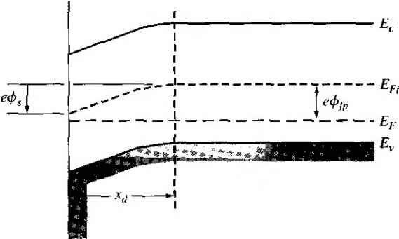 Figure П.8 (The energy-band diagram tn the p-type semiconductor, indicating surface potenrial. 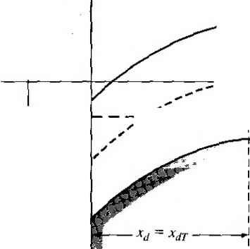 еф, - 2еф,-------- Figure 11.9 I The energy-band diagra semiconductor at the threshold in vers n in the Ptype on point. intrinsic level in the bulk semiconductor. The electron concentration at the surface is the same as the hole concentration in the bulk material. This condition is known as the threshold inversion point. The applied gate voltage creating this condition is known as the threshold voltage. If the gate voltage increases above this threshok value, the conduction band will bend slightly closer to the Fermi level, but change in the conduction band at the surface is now only a slight function of gat voltage. The electron concentration at the surface, however, is an exponential fui tion of the surface potential. The surface potential may increase by a few (кТ/е) volts, which will change the electron concentration by orders of magnitude, but space charge width changes only sUghtly. In this case, then, the space charge regit has essentially reached a maximum width. The maximum space charge width, xjr, at this inversion transition point can calculated from Equation (11.5) by setting 2фfp. Then 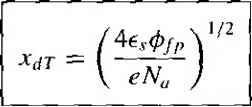 EXAMPLE 11.1 Objective To calculate the maximum space charge width given a particular semiconductor doping concentration. Consider silicon at 7 = 300 К doped to Nj = 10 cm~-. The intrinsic carrier concen tration is = 1.5 x 10 cm~. Щ Solution From Equation (11.4), we have /N \ / 10 \ 347 V Then the maximum space charge width is 4(1I.7)(8.85 X 10-)(0.347) (1.6 X 10-i*)(lO ) x,(T 0.30 X 10 cm = 0.30 fim Comment The maximum induced space charge width is on the same order of magnitude as pn junction space charge widths. We have been considering a p-type semiconductor substrate. The same maximum induced space charge region width occurs in an n-type substrate. Figure 11.10 is the energy-band diagram at the threshold voltage with an n-type substrate. We can write (11-7) (И-8) Note that we are always assuming the parameters and 0/ to be positive quantities. Figure 11.11 is a plot of х^т at T 300 К as a function of doping concentrarion in silicon. The semiconductor doping can be either n-type or p-type.
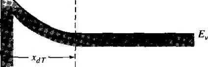 Figure 11.10 I The energy-band diagram in the n-type semiconductor at the threshold inversion point. 0,01 J i L U. 1 A 1. 1 7 - 300 К J I L. \ L 10 1qI6 iqJ7 V, semiconductor doping (cm ) Figure Н.И I Maximum induced space charge region width versus semiconductor doping. TEST YOUR UNDERSTANDING Ell.l (a) Consider as oxide-to-p-type siHcon junction at Г = 300 К. The impurity doping concentration in the siHcon is jV =3 x lO cmV Calculate the maximum space-charge width in the silicon, {b) Repeat part {a) for an impurity concentration of Л^ 10 cm- iwr/ ШЪ{Я) ш^08ГО(г^) Ell.2 Consider an oxide-to-n-type silicon junction at T = 300 K, The impurity doping concentration in the silicon is jVj = 8 x 10 cm~\ Calculate the maximum space-charge width in the siHcon. iiO UV) 11.1,3 Work Function Differences We have been concerned, so far, with the energy-band diagrams of the semiconduc- tor material. Figure 11.12a shows the energy levels in the metal, silicon dioxide, andj silicon relative to the vacuum level The metal work function is фщ and the electronj affinity is /. The parameter is the oxide electron affinity and, for silicon dioxiddj Xi = 0.9 V. 1 Figure 11.12b .shows the energy-band diagram of the entire metal-oxide-semiconductor structure with zero gate voltage applied. The Fermi level is a constant through the enrire system at thermal equilibrium. We may define as a modifiei metal work funcrion-the potenrial required to inject an electron from the metal int the conduction band of the oxide. Similarly, /is defined as a modified electron affinity. The voltage KiitO is the potential drop across the oxide for zero applied gal voltage and is not necessarily zero because of the difference between фщ and potenrial is the surface potential for this case. Metal , Уасиигп Jevel E.. - 9 eV -Epi Silicon dioxide p-typc silicon (a) Vacuum level Metal \ Oxide p-type semiconductor Oxide conduction band 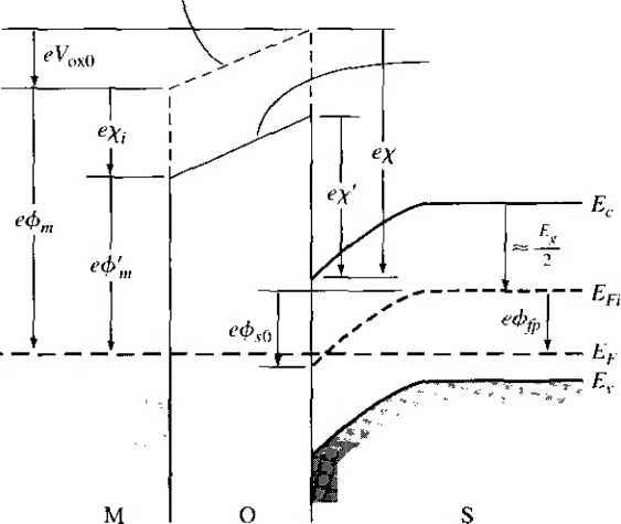 Figure 11Л2 I (a) Energy levels in an MOS system prior to contact and (b) energy-band diagram through the MOS structure in thermal equilibrium after contact. If we sum the energies from the Fermi level on the metal side to the Fermi level on the semiconductor side, we have eфso + еф/р (1E9) Equation (11.9) can be rewritten as We can define a potenrial 0 as 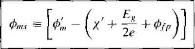 (11.10) (IMl) which is known as the metal-semiconductor work function difference. Objecrive example 11.2 To calculate the metal-semiconductor work function difference <, , for a given MOS systein and semiconductor doping. 1 ... 43 44 45 46 47 48 49 ... 55 |
||||||||||||
|
© 2026 AutoElektrix.ru
Частичное копирование материалов разрешено при условии активной ссылки |