 |
 |
 |
| Главная Журналы Популярное Audi - почему их так назвали? Как появилась марка Bmw? Откуда появился Lexus? Достижения и устремления Mercedes-Benz Первые модели Chevrolet Электромобиль Nissan Leaf |
Главная » Журналы » Absorbing materialorganic polymer 1 ... 44 45 46 47 48 49 50 ... 55 For an aluminium-sihcon dioxide junction, Ф1 = 3.20 V and for a silicon-siHcon dioxide junction, x = 3.25 V. We may assume that = 1T 1 eV. Let the p-type doping be Л' = 10 cm-\ Solution For silicon at Г = 300 К, we may calculate фfp as ф, = H in () = (0.0259) in {j) = 0.228 V Then the work function difference is 20- (3.25 4-0.555 + 0.228) = -0.83 V Comment The value of ф„, will become more negative as the doping of the p-type substrate increases. Degenerately doped polysilicon deposited on the oxide is also often used as the metal gate. Figure 11.13a shows the energy-band diagram of an MOS capacitor wit an n polysilicon gate and a p-type substrate. Figure 11.13b shows the energy-bai diagram for the case of a p+ polysilicon gate and the p-type silicon substrate. In the degenerately doped polysilicon, we will initially assume that Ef = Ec for the case and Ef - E for the p case. For the n * polysilicon gate, the metal-semiconductor work function difference can be written as 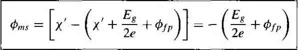 (U-12). n poly Ev -  О  p poly E, = E, - о
Figure 11.13 I Energy-band diagram through the MOS structure with a p-type substrate at zero gate bias for (a) an n+ polysilicon gate and (b) a p polysilicon gate. J and for the polysilicon gate, we have 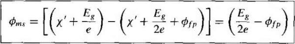 However, for degenerately doped n polysilicon and p polysilicon, the Fermi level can be above Ec and below E respectively, by 0.1 to 0.2 V. The experimental values will then be slightly different from the values calculated by using Equa-tions(ll.l2) and (11.13). , We have been considering a p-type semiconductor substrate. We may also have an n-type semiconductor substrate in an MOS capacitor. Figure 11.14 shows the energy-band diagram of the MOS capacitor with a metal gate and the n-type semiconductor substrate, for the case when a negative voltage is applied to the gate. The metal-semiconductor work function difference for this case is defined as (11.14) where ф[п is assumed to be a positive value. We will have similar expressions for n and p polysihcon gates. Figure II. 15 shows the work function differences as a function of semiconductor doping for the various types of gates. We may note that the magnitude of ф,пх for the polysilicon gates are somewhat brger than Equations (11.12) and (11.13) predict. This difference again is because the Fermi level is not equal to the conduction band 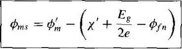 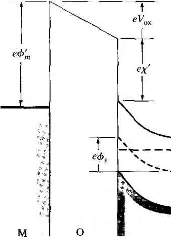 Figure 11.14 I Energy-band diagram throtigh the MOS structure with an n-type substrate for a negative applied gate bias. 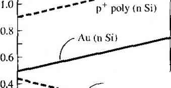 0.2 - -0.2 -0.4 -0.6 -0.8 t -1.0 10 p poly (p Si) Au(p Si)  poly (n Si) Al (n Si) Al (p Si) poly (p Si)  Figure 11.15 I Metal-semiconductor work function difference versus doping for aluminum, gold, and n * and p poJysilicon gates. {From Sze [I6j and Werner 119},) energy for the n * gate and is not equal to the valence band energy for the p gate. The metal-semiconductor work function difference becomes important in the flat-band, and threshold voltage parameters discussed next. TEST YOUR UNDERSTANDING E11.3 The si 1 icon i mpuri ty dop i ng concentration i n an al umin um-s i licon diox ide-sil icon MOS structure is /V 3 x 10 cm~\ Using the parameters in Example 11.2, determine the metal-semiconductor work function difference <, ,. A 1860 V) Ell.4 Consider an n polysilicon gate in an MOS structure with a p-type silicon substrate. The doping concentration of the silicon is N = 3 x 10 cm \ Using Equation (11.12), find the value of 0, ,. (A ie6*0- = suy) Ell .5 Repeal E11.4 for a p polysilicon gate using Equation {U.\3)AK6LV0 = V) 11,1.4 Flat-Band Voltage The flat-band voltage is defined as the applied gate voltage such that there is no band bending in the semiconductor and, as a result, zero net space charge in this region. Figure 11.16 shows this fiat-band condition. Because of the work function difference О Figure 1Ы6 I Energy-band diagram of an MOS capacitor at flat band. I and possible trapped charge in the oxide, the voUage across the oxide for this case is not necessarily zero. I We have implicitly been assuming that there is zero net charge density in the oxide material. This assumption may not be valid-a net fixed charge density, usu- ally positive, may exist in the insulator. The positive charge has been identified with broken or dangling covalent bonds near the oxide-semiconductor interface. During the thermal formation of SiOi, oxygen diffuses through the oxide and reacts near the Si-Si02 interface to form the Si02. Silicon atoms may also break away from the silicon material just prior to reacting to form SiOa. When the oxidation process is terminated, excess silicon may exist in the oxide near the interface, resulting in the dangling bonds. The magnitude of this oxide charge seems, in general, to be a strong function of the oxidizing conditions such as oxidizing ambient and temperature. The charge density can be altered to some degree by annealing the oxide in an argon or nitrogen atmosphere. However, the charge is rarely zero. The net fixed charge in the oxide appears to be located fairly close to the oxide-semiconductor interface. We will assume in the analysis of the MOS structure that an equivalent trapped charge per unit area, Q, is located in die oxide directly adjacent to the oxide-semiconductor interface. For the moment, we will ignore any other oxide-type charges that may exist in the device. The parameter Q is usually given in terms of number of electronic charges per unit area. Equation (11.10), for zero applied gate voltage, can be written as (1E15) If a gate voltage is applied, the potential drop across the oxide and the surface potential will change. We can then write Va = Д Vo, + Аф, - (Vox - Voxo) + (Фs - 0.0) (11.16) Using Equation (11.15), we have Vg - Vox + фs + Фrns (1E17) Figure U. 17 shows the charge distribution in the MOS structure for the flat-band condition. There is zero net charge in the semiconductor and we can assume that an equivalent fixed surface charge density exists in the oxide. The charge density on the metal is Q, and from charge neutrality we have QL + Qlso (11-18) p-type Metal Oxide semiconductor * EB. - ..: ... я,.... Figure 11.17 I Charge distribution in an MOS capacitor at fiat band. We can relate Q\ to the voltage across the oxide by с (11.19 where is the oxide capacitance per unit area. Substituting Equation (11.18) intt Equation (11.19), we have с In the flat-band condition, the surface potential is zero, or = 0. Then from Equa-; tion (11.17), we have Vn - (11.21J Equation (11.21) is the fiat-band voltage for this MOS device. EXAMPLE 11.3 Objective To calculate the flat-band voltage for an MOS capacitor with a p-type semiconductor substrate. Consider an MOS structure with a p-type semiconductor substrate doped to W, - 10 cm *, a silicon dioxide insulator with a thickness of fox = 5(Ю A, and an n polysilit gate. Assume that G = 10 electronic charges per cm-. Solution The work function difference, from Figure 1L15, is < = -IT V. The oxide capacitance c: be found as С - (3.9)(8.85 x 10-) , ----- = 6.9 x 10 F/cm 500 X 10-* Although we will, in general, use the primed notation for capacitance per unit area or charge per unit area, we will omit, for convenience, the prime on the oxide capacitance per unit area parameter. The equivalent oxide surface charge density is (10)(I.6 X 10 ) - 1.6 X 10- C/cnr The flat-band voltage is then calculated as Q:, . . /Кбх 10- с = -1.1 - 6.9 x 10- = -1.33 V Comment The applied gate vohagc required to achieve the flat-band condition for this p-type substrate is negative. If the amount of fixed oxide charge increases, the flat-band voltage becomes even more negative. TEST YOUR UNDERSTANDING El 1.6 Consider the MOS structure described in El 1.3. For an oxide thickness of t,y 200 A and an oxide charge of (2 = 8 x lO cm -, calculate the flat-band voltage. (Л 90 l - Д V) EH.7 Repeat El 1.6 for the MOS device described in El 1.4. (A ШТ- = V) E11.8 Repeat El 1.6 for the MOS device described in El 1.5. (A <;ОГО-Н = пу) ILLS Threshold Voltage The threshold voltage was defined as the applied gate voltage required to achieve the threshold inversion point. The threshold inversion point, in turn, is defined as the condition when the surface potential is = 2ф/р for the p-type semiconductor and 0, = 2ф1 for the n-type semiconductor. These conditions were shown in Figures 11.9a and 11.10. The threshold voltage will be derived in terms cf the electrical and geometrical properties of the MOS capacitor. Figure 11.18 shows the charge distribution through the MOS device at the threshold inversion point for a p-type semiconductor substrate. The space charge p-type
Figure 11.18 I Charge distribution in an MOS capacitor with a p-type substrate at the threshold inversion point. width has reached its maximum value. We will assume that there is an equivalent oxide charge Q and the positive charge on the metal gate at threshold is j2 y . The prime on the charge terms indicates charge per unit area. Even though we are assuming that the surface has been inverted, we will neglect the inversion layer charge at this threshold inversion point. From conservarion of charge, we can write (11.22) where e5£,(max) = €N XdT (11.23) and is the magnitude of the maximum space charge density per unit area of the depletion region. The energy-band diagram of the MOS system with an applied positive gate volt-age is shown in Figure 11.19. As we mentioned, an applied gate voltage will change the voltage across the oxide and will change the surface potential. We had from Equation (11Л 6) that Vo = AVox + ДФ. Vox -b + ф^п. At threshold, we can define Vq = tn* where Vtn is the threshold voltage that creates the electron inversion layer charge. The surface potential is ф^ = 2фfp at threshold so Equation (11.16) can be written as where Vyr the voltage across the oxide at this threshold inversion point. 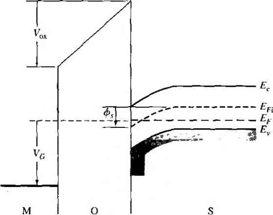 Figure 11Л9 f Energy-band diagram through the MOS structure with a positive applied gate bias. The voltage Vor can be related to the charge on the metal and to the oxide capacitance by с (11.25) where again Cox is the oxide capacitance per unit area. Using Equation (11.22), we can write Finally, the threshold voltage can be written as Q;- (max) Q;, + 0; v + 2ф/р (11-26) (11.27a) Vtn - (IQioCmax)! g;,) (-) + 0. + 20;, (П.27Ь) Using the definition of flat-band voltage from Equation (1L21), we can also express the threshold voltage as Vtn - G[-jr(max) 4- Vfb + 2фf, (11.27c) For a given semiconductor material, oxide material, and gate metal, the threshold voltage is a function of semiconductor doping, oxide charge Q, and oxide thickness. Objective To design the oxide thickness of an MOS system to yield a specified threshold voltage. Consider an n polysilicon gate and a p-type silicon substrate doped to N 3 x 10 cnr \ Assume 21 л = 10 cm~-. Determinethe oxide thickness such that Wa -1-0.65 V. Solution From Figure U. 15, the work function difference is 0 ,., = -1.13 V. The various parameters can be calculated as фfp V, In )=(0. 0259)In 3 x 10 \ Tx lOV 376 V 4(11.7)(8.85 X 10 i)(0-376) 1 (I.6 x 10-}(3 X lOj 1 0.18 дт Then DESIGN EXAMPLE 11.4  e;jj(max) = еК,х,г = (1.6 x 10 )(3 x I0)(0.18 x 10 ) 1е;(тах)1 = 8.64 x 10 C/cm The oxide thickness can be detennined from the threshold voltage equation Then [(8.64 X 10-)- (10)fl.6 X IQ-)! 0.65 =---!------ - - 1ЛЗ +2(0.376) (3.9)(8.85 x 10) 0.65 = 2.0 x 10 f -0.378 which yields rx = 504 A Comment The threshold voltage for this case is a positive quantity, which means that the MOS device is an enhancement mode device: a gate voltage must be applied to create the inversion layer charge, which is zero for zero applied gate voltage. The threshold voltage must be within the voltage range of a circuit design. Although we have not yet considered the current in an MOS transistor, the threshold voltage is the point at which the transistor turns on. If a circuit is to operate between 0 and 5 V and the threshold voltage of a MOSFET is 10 V, for example, the device and circuit cannot be turned on and *off. The threshold voltage, then, is one of the important parameters of the MOSFET. EXAMPLE 11.5 Objective To calculate the threshold voltage of an MOS system using the aluminum gate. Consider a p-type silicon substrate at T = 300 К doped to = 10 * cm. Let gj = 10 cm . - 500 A, and assume the oxide is silicon dioxide. From Figure 11.15, we have that ф^ = 0.83 V. Solution We can start calculating the various parameters as 0.228 V
= 2.43 Mm Then e;,(max) =eiV,jrrfr = (L6 x 10-)(Ш^)(2.43 x Ю **) 3.89 x 10* C/cm We can now calculate the threshold voltage as = [(3.89 X 10-) - (10 )(l-6 X 10-)] -0.83+2(0.228) 500 X 10 Д3.9)(8.85 X 10-) = - 0.341 V Comment In this example, the semiconductor is very lightly doped which, in conjunction with the positive charge in the oxide and the work function potential difference, is sufficient to induce an electron inversion layer charge even with zero applied gate voltage. This condition makes the threshold voltage negative. A negative threshold voUage for a p-type substrate implies a depletion mode device. A negative voltage must be applied to the gate in order to make the inversion layer charge equal to zero, whereas a positive gate voltage will induce a larger inversion layer charge. Figure 11.20 is a plot of the threshold voltage Vtn as a function of the acceptor doping concentration for various positive oxide charge values. We may note that the p-type semiconductor must be somewhat heavily doped in order to obtain an enhancement mode device. The previous derivation of the threshold voltage assumed a p-type semiconductor substrate. The same type of derivation can be done with an n-type semiconductor substrate, where a negative gate voltage can induce an inversion layer of holes at the oxide-semiconductor interface. Figure 11.14 showed the energy-band diagram of the MOS structure with an n-type substrate and with an applied negative gate voltage. The threshold voltage for this case can be derived and is given by VrP-(-Q:,o(max)bQ:, (11.28) where li25o(max) = eNdXtiT (11.29a) (11.29b) (11.29c) 1 ... 44 45 46 47 48 49 50 ... 55 |
|||||||||||||||||||||||||||||||||||||||
|
© 2026 AutoElektrix.ru
Частичное копирование материалов разрешено при условии активной ссылки |