 |
 |
 |
| Главная Журналы Популярное Audi - почему их так назвали? Как появилась марка Bmw? Откуда появился Lexus? Достижения и устремления Mercedes-Benz Первые модели Chevrolet Электромобиль Nissan Leaf |
Главная » Журналы » Absorbing materialorganic polymer 1 ... 45 46 47 48 49 50 51 ... 55 о >
3 (cm- Ъ Figure 11.201 Threshold voltage of an n-channel MOSFET versus the p-type substrate doping concentration for various values of oxide trapped charge {ty, 500 A, aluminum gate). 0/ V; In (11.29d) We may note that л^г and ф/п are defined as positive quantities. We may also note that the notation of Vjp is the threshold voltage that will induce an inversion layer of holes. We will later drop the N and P subscript notation on the threshold voltage, but, for the moment, the notation may be useful for clarity. DESIGN EXAMPLE 11.6  Objective To design the semiconductor doping concentration to yield a specified threshold voltage. Consider an aluminum-silicon dioxide-silicon MOS structure. The silicon is n type, the oxide thickness is /ox = 650 A, and the trapped charge density is = 10 cm -. Determine the doping concentration such that Vtp = - LO V. Solution The solution to this design problem is not straightforward, since the doping concentration appears in the terms ф/ ,х^г, Q(max) and ф^ . The threshold vohage, then, is a nonlinear function of Nt{. Without a computer-generated solution, we resort to trial and error. For = 2.5 x 10 cпl- we find 0y = V, In 0.253 V = F62 fim XdT = Then IG;.J(max)l = eJVAVr = 6.48 x 10 C/cm From Figure 11.15, ф^, = -035 V The threshold voltage is Утр = (-lesz/niax)! - Qj jj +0... -20y, [-(6.48 x 10-) - (10 )(L6 X 10**)](650 x lO ) - 0.35 - 2(0.253) (3,9)(8.85 X 10--) which yields Утр = -1.008 V and is essentially equal to the desired result. Comment The threshold voltage is negative, implying that this MOS capacitor, with the n-type substrate, is an enhancement mode device. The inversion layer charge is zero with zero gate voltage, and a negafive gate voltage must be applied to induce the hole inversion layer. Figure 11.21 is a plot of Vtf versus doping concentration for several values of - We may note that, for all values of positive oxide charge, this MOS capacitor is always an enhancement mode device. As the charge increases, the threshold voltage becomes more negative, which means that it takes a larger applied gate voltage to create the inversion layer of holes at the oxide-semiconductor interface. 11Л .6 Charge Distribution Weve discussed the various charges in the MOS structure. We may gain a better understanding by considering the following figures. The electron concentration in the inversion layer (p-type substrate) at the oxide interface is given by . - (nj/Na) exp(</>v/Vf). For silicon at Г = 300 К with an impurity doping concentration of Л' = 1 X 10 cm-, the surface potential at the threshold inversion point is Ф, - 2фff, - 0.695 V. The electron concentration at the oxide interface at this surface potential is just = I x 10 cm- as we have discussed before. Figure 11.22 с >
Figure 11.211 Threshold voltage of a p-channcl MOSFET versus the n-type substrate doping concentration for various values of oxide trapped charge (tt = 500 A, aluminum gate). 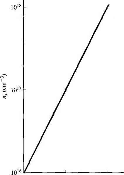 2фJp (2ф^р + 0.06) {2ф^, + 0.12) Ф, (volts) Figure 11.22 I Electron inversion charge density as a function of surface potential. p-type Si (300 K) 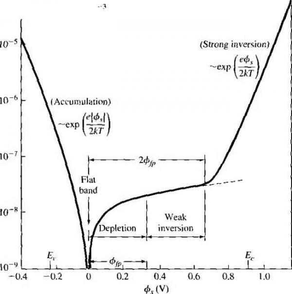 Figure 11.23 I Variation of surface charge density (accumulation charge and inversion charge) as a function of surface potential. (From Sze 116}.) shows the increase in electron concentration at the surface with an increase in surface potential- As discussed previously, since the electron concentration increases rapidly with very small changes in surface potential, the space charge v/idth has essenrially reached a maximum value. Figure 11.23 shows the total charge density (C/cm ) in the silicon as a function of the surface potential. At flat band, the total charge is zero. For 0 < 0 < ф/р, we are operating in the depletion mode since the inversion charge has not yet been formed. For ф^р < < 2фfp, the Fermi energy at the surface is in the upper half of the band diagram, which implies an n-type material, but we have not yet reached the threshold inversion point. This condition is referred to as weak inversion. The condition for 0j > 2ф/р is called strong inversion, since the inversion charge density increases rapidly with an increase in surface potential, as we have seen. TEST YOUR UNDERSTANDING ЕП,9 An MOS device has the following parameters: aluminum gate, p-type substrate with iV 3 X 10* cm- \ /ox = 250 A, and Q = 10 cm -. Determine the threshold voltage. (A *suv) Е11Л0 Consider an MOS device with the following parameters: p polysilicon gate, n-type subsu-ate with = 10- cm /x = 220 A, and 8x10 cm (Use Figure 11Л5). Determine the threshold voltage. (Л t3Z0+ *иу) *E11.11 The device described in E11Л 0 is to be redesigned by changing the n-type doping concentration such that the threshold voltage is in the range 0.50 Vj < -0.30 V, (tuiD giOl X 17 - Л/ m A ЯОГО- - *Jt)xi3 рпБ \VAX\ -suv) 11.2 I CAPACITANCEVOLTAGE CHARACTERISTICS The MOS capacitor structure is the heart of the MOSFET. A great deal of information about the MOS device and the oxide-semiconductor interface can be obtains from the capacitance versus voltage or C-V characteristics of the device. The ca[ itance of a device is defined as C=~ (11.30 where dQ \s the magnitude of the differential change in charge on one plate as al function of the differential change in voltage dV across the capacitor. The capaci-j tance is a small-signal or ac parameter and is measured by superimposing a small ac voltage on an applied dc gate voltage. The capacitance, then, is measured as a func-i tion of the applied dc gate voltage. 11.2Л Ideal C-V Characteristics First we will consider the ideal C-V characteristics of the MOS capacitor and thenl discuss some of the deviations that occur from these idealized results. We will ini-tially assume that there is zero charge trapped in the oxide and also that there is no charge trapped at the oxide-semiconductor interface. There are three operating conditions of interest in the MOS capacitor: accumulation, depletion, and inversion. Figure 11.24a shows the energy-band diagram of an MOS capacitor with a p-type substrate for the case when a negative voltage is applied to the gate, inducing an accumulation layer of holes in the semiconductor at the oxide-semiconductor interface. A small differential change in voltage across the MOS structure will cause a differential change in charge on the metal gate and also in the hole accumulation charge, as shown in Figure 11.24b. The differential changes in charge density occur at the edges of the oxide, as in a parallel-plate capacitor. The capacitance С per unit area of the MOS capacitor for this accumulation mode is just the oxide capacitance, or C4acc)-Cox-- (11.31) Figure 11.2 5a shows the energy-band diagram of the MOS device when a small positive voltage is applied to the gate, inducing a space charge region in the semiconductor; Figure 11.25b shows the charge distribution through the device for Metal Oxide p-type semiconductor -Q -\dQ-\ -I \dQ + Q Figure 11.24 1 (a) Energy-band diagram through an MOS capacitor for the accumulation mode, (b) Differential charge distribution at accumulation for a differential change in gate voltage. Metal Oxide p-type semiconductor
Figure 11.25 I (a) Energy-band diagram through an MOS capacitor for the depletion mode, (b) Differential charge distribution at depletion for a differential change in gate voltage. this condition. The oxide capacitance and the capacitance of the depletion region are in series. A small differential change in voltage across the capacitor will cause a differentia] change in the space charge width. The corresponding differential changes in charge densities are shown in the figure. The total capacitance of the series combinarion is 1 1 C(depl) Cox C, (11.32a) C(depl)= Co. + С (11.32b) Since Cox - ox/tox and C = cjx. Equation (1 L32b) can be written as С C4depl) (11.33 As the space charge width increases, the total capacitance C(depl) decreases. We had defined the threshold inversion point to be the condition when the maximum depletion width is reached but there is essentially zero inversion charge density. This condition will yield a minimum capacitance C- which is given by C - 4>X (11341 Figure 11.26a shows the energy-band diagram of this MOS device for the inver sion condition. In the ideal case, a small incremental change in the voltage across the MOS capacitor will cause a differential change in the inversion layer charge density. The space charge width does not change. If the inversion charge can respond to the change in capacitor voltage as indicated in Figure 11.26b, then the capacitance i again just the oxide capacitance, or C4inv) = Cox = - Figure 11.27 shows the ideal capacitance versus gate voltage, or C-V, character istics of the MOS capacitor with a p-type substrate. The three dashed segments corn respond to the three components Cox, sd min- curve is the ideal net capacitance of the MOS capacitor. Moderate inversion, which is indicated in the figure, is the transition region between the point when only the space charge density Metal Oxide p-type semiconductor 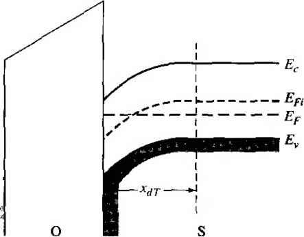
(b> Figure 11.26 I (a) Energy-band diagram through an MOS capacitor for the inversion mode, (b) Differential charge distribution at inversion for a low-frequency differential change in gate voltage. Ассити]т'юп Depletion 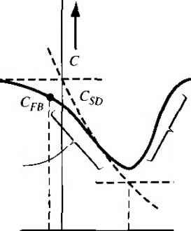 Strong inversion Moderate inversion С Figure 11.271 Ideal low-frequency capacitance versus gate voltage of an MOS capacitor with a p-type substrate. Individual capacitance components are also shown. changes with gate voltage and when only the inversion charge density changes with gate voltage. The point on the curve that corresponds to the flat-band condition is of interest. The flat-band condition occurs between the accumulation and depletion conditions. The capacitance at flat band is given by 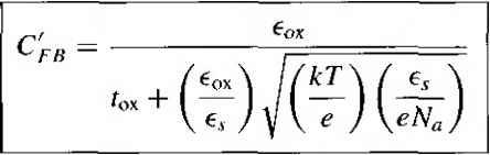 (11.36) We may note that the flat-band capacitance is a function of oxide thickness as well as semiconductor doping. The general location of this point on the C-V plot is shown in Figure 11.27. Objective To calculate Сок C, and Cr for an MOS capacitor. Consider a p-type silicon substrate at T = 300 К doped to Л^ = 10 cm The oxide is silicon dioxide with a thickness of 550 A and the gate is aluminum. Solution The oxide capacitance is Cox - - (3.9)(8.S5 x 10-) 550 x 10-s To find the minimum capacitance, we need to calculate = V, in (0.0259) .n(J)= 0.2 347 V EXAMPLE1E7 XdT - 4(11.7){8.85 X 10(0.347) (1.6 X 10-)(10i) 0.30 X 10- cm Then С = (3.9)(8.85 X 10 ) xT (550 x 10-) + = 2.23 X 10 fW! (0.3 X 10-) We may note that C. 2.23 X 10- 6.28 X 10- The flat-band capacitance is fb - fox + (3.9)(8.85 X 10 *) (550 x 10-) + f- 5.03 x 10-* Vhm-  (1.6 x 10-Ъ(10Ъ We may also note I hat C 5.03 x 10- t в - 0 80 Q 6.28 x 10- Comment The ratios of C, to and of CJ,j to Qx are typical values obtained in C-V plots. TEST YOUR UNDERSTANDING Ell.12 For the device described in El 1.9, determine C/Ci,x and Cjr Cox Typical values of channel length and width are 2 )uni and 20 jum, respectively. The total gate oxide capacitance for this example is then CoxT = (6.28 X 10-)(2 X 10 -)(20 x 10 ) = 0.025 x lO F = 0.025 pF The total oxide capacitance in a typical MOS device is quite small. The same type of ideal C-К characteristics are obtained for an MOS capacitor with an n-type substrate by changing the sign of the voltage axis. The accumulation Strong inversion Moderate inversion 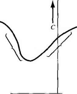 Accumulation Depletion Figure 11.28 I Ideal low-frequency capacitance versus gate voltage of an MOS capacitor with an n-type substrate. condition is obtained for a positive gate bias and the inversion condition is obtained for a negative gate bias. This ideal curve is shown in Figure 11.28. 11.2.2 Frequency Effects Figure 11.26a showed the MOS capacitor with a p-type substrate and biased in the inversion condition. We have argued that a differential change in the capacitor voltage in the ideal case causes a differential change in the inversion layer charge density. However, we must consider the source of electrons that produces a change in the inversion charge density. There are two sources of electrons that can change the charge density of the inversion layer The first source is by diffusion of minority carrier electrons from the p-type substrate across the space charge region. This diffusion process is the same as that in a reverse-biased pn junction that generates the ideal reverse saturation current. The second source of electrons is by thermal generarion of electron-hole pairs within the space charge region. This process is again the same as that in a reverse-biased pn junction generating the reverse-biased generation current. Both of these processes generate electrons at a particular rate. The electron concentration in the inversion layer, then, cannot change instantaneously. If the ac voltage across the MOS capacitor changes rapidly, the change in the inversion layer charge will not be able to respond. The C-V characteristics will then be a function of the frequency of the ac signal used to measure the capacitance. In the limit of a very high frequency, the inversion layer charge will not respond to a differential change in capacitor voltage. Figure 11.29 shows the charge distribution in the MOS capacitor with a p-type substrate. At a high-signal frequency, the differential change in charge occurs at the metal and in the space charge width in the semiconductor. The capacitance of the MOS capacitor is then Ci, which we discussed earlier. The high-frequency and low-frequency limits of the C-V characteristics are shown in Figure 11.30. In general, high frequency corresponds to a value on the order 1 ... 45 46 47 48 49 50 51 ... 55 |
||||||||||||||||||||||||||||||||||||||||||||||||||||||||||||||||||||
|
© 2026 AutoElektrix.ru
Частичное копирование материалов разрешено при условии активной ссылки |