 |
 |
 |
| Главная Журналы Популярное Audi - почему их так назвали? Как появилась марка Bmw? Откуда появился Lexus? Достижения и устремления Mercedes-Benz Первые модели Chevrolet Электромобиль Nissan Leaf |
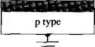
Главная » Журналы » Absorbing materialorganic polymer 1 ... 46 47 48 49 50 51 52 ... 55 Metal Oxide p-type semiconductor Figure 11.29 I Differential charge distribution at inversion for a high-frequency differential change in gate voltage. Accumulation 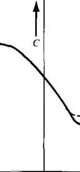 Low frequency High frequency Inversion Figure 11.30 I Low-frequency and high-frequency capacitance versus gate voltage of an MOS capacitor with a p-type substrate. of 1 MHz and low frequency corresponds to values in the range of 5 to 100 Hz. Typically, the high-frequency characteristics of the MOS capacitor are ineasured. 11.23 Fixed Oxide and Interface Charge Effects In all of the discussion concerning C-Vcharacteristics so far, we have assumed an ideal oxide in which there are no fixed oxide or oxide-semiconductor interface charges. These two types of charges will change the C-V characteristics. We previously discussed how the fixed oxide charge affects the threshold voltage. This charge will also affect the flat-band voltage. The flat-band voltage from Equation (11.21) was given by where is the equivalent fixed oxide charge and ф^ is the metal-semiconductor work function difference. The flat-band voltage shifts to more negative voltages for a positive fixed oxide charge. Since the oxide charge is not a function of gate voltage, the curves show a parallel shift with oxide charge, and the shape of the C-V curves remains the same as the ideal characteristics. Figure 11.31 shows the high-frequency characteristics of an MOS capacitor with a p-type substrate for several values of fixed positive oxide charge. The C-V characteristics can be used to determine the equivalent fixed oxide charge. For a given MOS structure, , and Cx are known, so the ideal flat-band voltage and flat-band capacitance can be calculated. The experimental value of flat-band voltage can be measured from the C-V curve and the value of fixed oxide charge can then be determined. The C-V measurements are a valuable diagnostic tool to characterize an MOS device. This characterization is especially useful in the study of radia-fion effects on MOS devices, for example, which we will discuss in the next chapter. We first encountered oxide-semiconductor interface states in Chapter 9 in the discussion of Schottky barrier diodes. Figure 11.32 shows the energy-band diagram of a semiconductor at the oxide-semiconductor interface. The periodic nature of the semiconductor is abruptly terminated at the interface so that allowed G\QCtronic energy levels will exist within the forbidden bandgap. These allowed energy states are referred to as interface states. Charge can flow between the semiconductor and interface states, in contrast to the fixed oxide charge. The net charge in these interface states is a function of the posirion of the Fermi level in the bandgap. In general, acceptor states exist in the upper half of the bandgap and donor states exist in the lower half of the bandgap. An acceptor state is neutral if the Fermi level Q\s>Q\s2 Qs.2><\si С>;.г>0 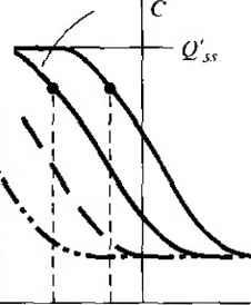 = 0 (ideal) с ITlin Allowed electronic energy states Acceptor states Donor slates tigure 11.31 I High-frequency capacitance versus gate voltage of an MOS capacitor with a p-type substrate for several values of effective trapped oxide charge. Figure 11.32 I Schemafic diagram showing interface states at the oxide-semiconductor interface. is below the state, and becomes negatively charged if the Fermi level is above the state. A donor state is neutral if the Fermi level is above the state and becomes positively charged if the Fermi level is below the state. The charge of the interface states is then a function of the gate voltage applied across the MOS capacitor. Figure 11.33a shows the energy-band diagram in a p-type semiconductor of an MOS capacitor biased in the accumulation condition. In this case, there is a net positive charge trapped in the donor states. Now let the gate voltage change to produce the energy-band diagram shown in Figure 11.33b. The Fermi level corresponds to the intrinsic Fermi level at the surface; thus, all interface states are neutral. This Neutral acceptors Positive tlonors Neutral donors Neutral acceptors Neutral donors 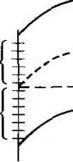 Neutral acceptors Negati acceptors live Г [ors I Neutral donors 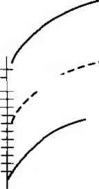 Figure 1ЬЗЗ I Energy-band diagram in a p-type semiconductor showing the charge trapped in the interface states when the MOS capacitor is biased (a) in accumulation, (b) at midgap, and (c) at inversion. 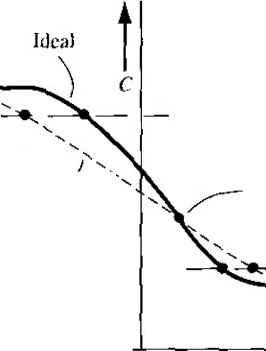 With interface states C/,;j (Hat-band) Midgap ThrcshoJd Figure 11.34 I High-frequency C-V characteristics of an MOS capacitor showing effects of interface states. particular bias condition is known as midgap. Figure 11.33c shows the condition at inversion in which there is now a net negative charge in the acceptor states. The net charge in the interface states changes from positive to negative as the gate voUage sweeps from the accumulation, depletion, to the inversion condition. We noted that the C-V curves shifted in the negative gate voltage direction due to positive fixed oxide charge. When interface states are present, the amount and direction of the shift changes as we sweep through the gate voltage, since the amount and sign of the interface trapped charge changes. The C-V curves now become smeared ouf as shown in Figure 11.34. Again, the C-V measurements can be used as a diagnostic tool in semiconductor device process control. For a given MOS device, the ideal C-V curve can be determined. Any smearing out in the experimental curve indicates the presence of interface states and any parallel shift indicates the presence of fixed oxide charge. The amount of smearing out can be used to determine the density of interface states. These types of measurement are extreinely useful in the study of radiation effects on MOS devices, which we will consider in the next chapter. 11.3 I THE BASIC MOSFET OPERATION The current in an MOS field-effect transistor is due to the flow of charge in the inversion layer or channel region adjacent to the oxide-semiconductor interface. We have discussed the creation of the inversion layer charge in enhancement-type MOS capacitors. We may also have depletion-type devices in which a channel already exists at zero gate voltage. 113.1 MOSFET Structures There are four basic MOSFET device types. Figure 11.35 showsan n-channel enhancement mode MOSFET. Implicit in the enhancement mode notation is the idea that the semiconductor substrate is not inverted directly under the oxide with zero gate; voltage. A positive gate voltage induces the electron inversion layer, which then connects the n-type source and the n-type drain regions. The source terminal is the source of carriers that flow through the channel to the drain terminal. For this n-channel device, electrons flow from the source to the drain so the conventional current will enter the drain and leave the source. The conventional circuit symbol for this n~channel enhancement mode device is also shown in this fieure. Figure 11.36 shows an n-channel depletion mode MOSFET. An n-channel region exists under the oxide with zero volts applied to the gate. However, we have shown that the threshold voltage of an MOS device with a p-type substrate may be Source fS) Gate (G) Drain (D) ООО 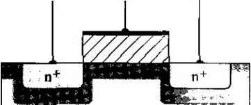 Substrate or body (B) В Figure 11.35 I Cross section and circuit symbol for an n-channel enhancement-mode MOSFET. Source (S) Gate (G) Drain (D) ооо 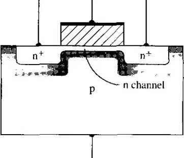 В О Body (В) Figure 11.361 Cross section and circuit symbol for an n-channel depletion-mode MOSFET. negative; this means that an electron inversion layer already exists with zero gate voltage appHed. Such a device is also considered to be a depletion inode device. The n-channel shown in this figure can be an electron inversion layer or an intentionally doped n-region- The conventional circuit symbol for the n-channel depletion mode MOSFET is also shown in the figure. Figures 11.37a and 11.37b show a p-channel enhancement mode MOSFET and a p-channel depletion inode MOSFET. In the p-channel enhancement mode device, a negative gate voltage must be applied to create an inversion layer of holes that will connect* the p-type source and drain regions. Holes flow from the source to the drain, so the conventional current will enter the source and leave the drain. A p-channel region exists in the depletion mode device even with zero gate voltage. The conventional circuit symbols are shown in the figure. Source (S) Gale (G) Drain (D) ООО 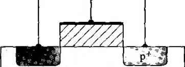 -В Body (B) Source (S) Gate (G) Drain (D) 0 9 9  p channel В Body (B) Figure U.371 Cross section and circuit symbol for (a) a p-channel enhancement mode MOSFET and (b) a p-channel deplefion mode MOSFET. 11.3,2 Current-Voltage Relationship-Concepts Figure 11.38a shows an n-channel enhancement mode MOSFET with a gate-t source voltage that is less than the threshold voltage and with only a very si drain-to-source voltage. The source and substrate, or body, terminals are held ground potential. With this bias configuration, there is no electron inversion layc the drain-to-substrate pn junction is reverse biased, and the drain current is zero (dii regarding pn junction leakage currents). Figure 11.38b shows the same MOSFET with an applied gate voltage such Vg5 > V7. An electron inversion layer has been created so that, when a small draii voltage is applied, the electrons in the inversion layer will flow from the source to positive drain terminal. The conventional current enters the drain terminal and leav< the source terminal. In this ideal case, there is no current through the oxide to the gat terminal. For small Vos values, the channel region has the characteristics of a resistor, we can write where is defined as the channel conductance in the limit as Vos ~ 0. The chani conductance is given by (11.31 where Дд is the mobility of the electrons in the inversion layer and Q \ is the mi nitude of the inversion layer charge per unit area. The inversion layer charge is a function of the gate voltage; thus, the basic MOS transistor action is the modulation of the channel conductance by the gate voltage. The channel conductance, in tu: . determines the drain current. We will initially assume that the mobility is a constant; we will discuss mobility effects and variations in the next chapter. 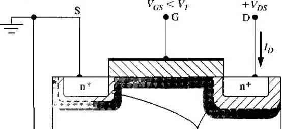 У as > Vr Space ctiarge regions 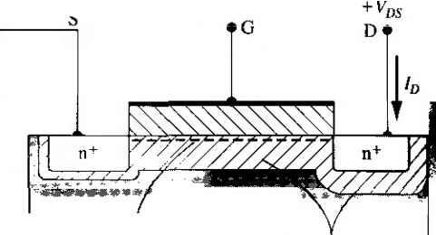 Induced electron inversion layer Space charge regions Figure 11.38 I The n-channel enhancement mode MOSFET (a) with an applied gate voltage Vcs < Vt , and (b) with an applied gate voltage Vcs > Vr, The ]o versus Yds characteristics, for sinalJ values of Vis, are shown in Figure 11.39. When Vqs < Vr, the drain current is zero. As Vcs becomes larger than Vr, channel inversion charge density increases, which increases the channel conductance. A larger value of gj produces a larger initial slope of the I о versus Vs characteristic as shown in the figure. Figure 11.40a shows the basic MOS structure for the case when Vcs > Vr and the applied Vos voltage is small. The thickness of the inversion channel layer in the figure qualitatively indicates the relative charge density, which is essentially constant along the entire channel length for this case. The corresponding I о versus Vos curve is shown in the figure. Figure 11.40b shows the situation when the Yds value increases. As the drain voltage increases, the voltage drop across the oxide near the drain terminal decreases, which means that the induced inversion charge density near the drain also decreases. The incremental conductance of the channel at the drain decreases, which then means that the slope of the Id versus Vps curve will decrease. This effect is shown in the 11) versus Yds curve in the figure. When Vos increases to the point where the potenrial drop across the oxide at the drain terminal is equal to Vj, the induced inversion charge density is zero at the drain terminal. This effect is schematically shown in Figure 11.40c. At this point, the incremental conductance at the drain is zero, which means that the slope of the versus Vos curve is zero. We can write Vcs - V5(sat) Vj (11.39a) VDs(sat) = Vcs - Vj (11.39b) where Vds(3) i*> the drain-to-source voltage producing zero inversion charge density at the drain terminal. Vas > Vr 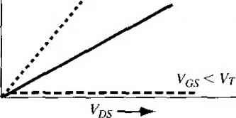 Figure IL39} versus Vrjs characteristics for small values of Vs at three Vcs voltages. 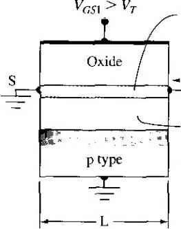 Vgs, Oxide ptype Channel inversion charge Depletion region 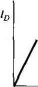 Vds Channel inversion charge
 inversion charge 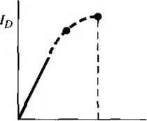 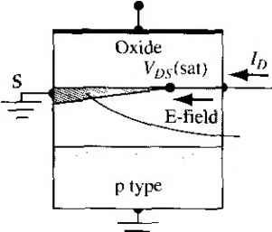 Channel inversion charge 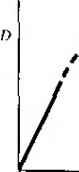 Saturation region Figure 11.40! Cross section and /d versus Vs curve wher\ Vq s < V7 for (a) a small Vos value, (b) a larger Vos value, (c) a value of Vd5 - VCsat), and (d) a value of Vos > (sat). When becomes larger than the V/j)5(sat) value, the point in the channel at which the inversion charge is just zero moves toward the source terminal. In this case, electrons enter the channel at the source, travel through the channel toward the dmn, and then, at the point where the charge goes to zero, the electrons are injected into the space charge region where they are swept by the E-field to the drain contact. If we assume that the change in channel length AL is small compared to the original length then the drain current will be a constant for Vs > /(sat). The region of the I о versus Vqs characteristic is referred to as the saturation region. Figure 11.40d shows this region of operation. When Vqs changes, the versus Vos curve will change. We saw that, if Vs increases, the initial slope of lo versus Vos increases. We can also note from Equation (11,39b) that the value of V/s(sat) is a function of Vgs* We can generate the family of curves for this n-channel enhancement mode MOSFET as shown in Figure 11.41. Figure 11.42 shows an n-channel depletion mode MOSFET. If the n-channel region is actually an induced electron inversion layer created by the metal-semiconductor work function difference and fixed charge in the oxide, the current-voltage characteristics are exactly the same as we have discussed, except that Vj is a negative quantity. We may also consider the case when the n-channel region is actually an n-type semiconductor region. In this type of device, a negative gate voltage will induce a space charge region under the oxide, reducing the thickness of the n-channel region. The reduced thickness decreases the channel conductance, which reduces the drain current. A positive gate voltage will create an electron accumulation layer, which increases the drain current. One basic requirement for this device is that the channel thickness tc must be less than the maximum induced space charge width in order to be able to turn the device off. The general I о versus Vos family of curves for an n-channeJ depletion mode MOSFET is shown in Figure 11.43. 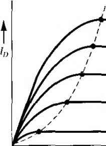 Vd5<0 - gs - Ут У05Ъ > УоЛ VGi4 > VgS2 GS > VOSI У OS! > Vgs\ Vds- Figure 11.41 I Family of versus Vos curves for an n-channel enhancement-mode MOSFET 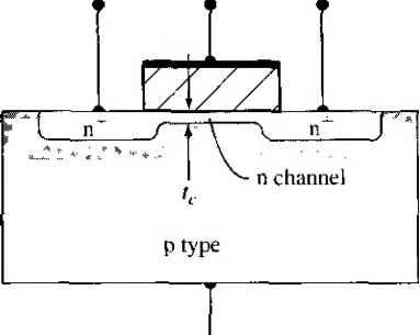 В Figure 1L42 I Cross section of an n-channel depletion-mode MOSFET. 1 ... 46 47 48 49 50 51 52 ... 55 |
|
© 2026 AutoElektrix.ru
Частичное копирование материалов разрешено при условии активной ссылки |