 |
 |
 |
| Главная Журналы Популярное Audi - почему их так назвали? Как появилась марка Bmw? Откуда появился Lexus? Достижения и устремления Mercedes-Benz Первые модели Chevrolet Электромобиль Nissan Leaf |
Главная » Журналы » Absorbing materialorganic polymer 1 ... 5 6 7 8 9 10 11 ... 55 Ш Comment We see from Figure 3.8c that, as the energy increases, the widths of the allowed bands increase from this Kronig-Penney model. TEST YOUR UNDERSTANDING ЕЗЛ Using the parameters given in Example 3.2, determine the width (in eV) of the forbidden energy band that exists aika - тг (see Figure 3.8c). (Л^ 6Z, = Я V *suv) Consider again the right side of Equation (3.24), which is the function cos ka. The cosine funcdon is periodic so that cos ka = cos (ka + 2пя) = cos (ka - Inn) (331) where w is a positive integer. We may consider Figure 3.9 and displace portions of the curve by 27Г. Mathematically, Equation (3.24) is still satisfied. Figure 3.10 shows how various sQg;mmts of the curve can be displaced by the 2n factor. Figure 3.11 shows the case in which the entire E versus к plot is contained within -я/а < к <n/a. This plot is referred to as a reduced space diagram, or a reduced-zero representation. We noted in Equation (3.27) that for a free electron, the particle momentum and the wave number к are related by p = hk. Given the similarity between the free   H к ti Figure ЗЛО 1 The £ versus к diagram showing 2jr displacements of several secfions of allowed energy bands. Reduced к space Figure ЗЛ11 The E versus к diagram in the reduced-zone representafion. electron solution and the results of the single crystal shown in Figure 3.9, the parameter hk in a single crystal is referred to as the crystal momentum. This parameter is not the actual momentum of the electron in the crystal, but is a constant of the mo- ; tion that includes the crystal interaction. We have been considering the Kronig-Penney model, which is a one-dimensional periodic potential function used to model a single-crystal lattice. The principle result of this analysis, so fan is that electrons in the crystal occupy certain allowed energy bands and are excluded from the forbidden energy bands. For real three-dimensional single-crystal materials, a similar energy-band theory exists. We will obtain additional electron properties from the Kronig-Penney model in the next sections. 3.2 I ELECTRICAL CONDUCTION IN SOLIDS Again, we are eventually interested in determining the current-voltage characteristics of semiconductor devices. We will need to consider electrical conduction in solids as h relates to the band theory we have just developed. Let us begin by considering the motion of electrons in the various allowed energy bands. 3.2.1 The Energy Band and the Bond Model In Chapter I, we discussed the covalent bonding of silicon. Figure 3.12 shows a two-dimensional representation of the covalent bonding in a single-crystal silicon lattice. This figure represents silicon at Г = 0 К in which each silicon atom is surrounded by eight valence electrons that are in their lowest energy state and are directly involved in the covalent bonding. Figure 3.4b represented the splitting of the discrete silicon energy states into bands of allowed energies as the silicon crystal is formed. At Г - 0 K, the 4N states in the lower band, the valence band, are filled with the valence electrons. All of the valence electrons schematically shown in Figure 3.12 are in the valence band. The upper energy band, the conduction band, is completely empty at Г = 0 K. II и ir II II ii и и и II ri =-o=o=o=o-= ===o=o=o=o=== ===o=o=o=o=== II II Figure 3.12 J Two-dimensional representation of the covalent bonding in a semiconductor at Г = 0 K. As the temperature increases above 0 K, a few valence band electrons may gain enough thermal energy to break the covalent bond and jump into the conduction band. Figure ЗЛЗа shows a two-dimensional representation of this bond-breaking effect and Figure ЗЛЗЬ, a simple line representation of the energy-band model, shows the same effect. The semiconductor is neutrally charged. This means that, as the negatively charged electron breaks away from its covalent bonding position, a positively charged empty state is created in the original covalent bonding position in the valence band. As the temperature further increases, more covalent bonds are broken, more electrons jump to the conduction band, and more positive empty states are created in the valence band. We can also relate this bond breaking to the E versus k energy bands. Figure ЗЛ4а shows the E versus к diagram of the conduction and valence bands at 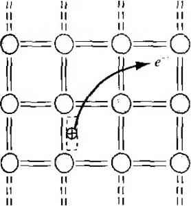 Conduction band Valence band  Figure ЗЛЗ I (a) Two-dimensional representation of the breaking of a covalent bond, (b) Corresponding line representation of the energy band and the generation of a negative and positive charge with the breaking of a covalent bond. 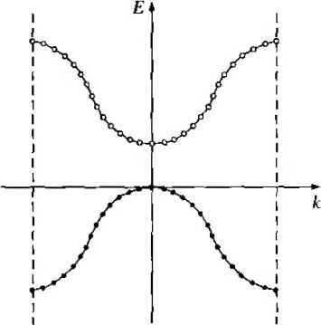  Figure ЗЛ4 i The E versus к diagram of the conduction and valence bands of a semiconductor at (a) Г 0 К and (b) Г > 0 К. J =qVi (3.33) where d, is the velocity of the ah ion. The summation in Equation (3.33) is taken over a unit volume so that the current density / is still in units of A/cm. Since electrons are charged particles, a net drift of electrons in the conduction band will give rise to a current. The electron distribution in the conduction band, as shown in Figure 3.14b, is an even function of к when no external force is applied. Recall that к for a free electron is related to momentum so that, since there are as many electrons with a -\k\ value as there are with a - value, the net drift current density due to these electrons is zero. This result is ceitainly expected since there is no externally applied force. If a force is applied to a particle and the particle moves, it must gain energy. This effect is expressed as dE = Fdx = Fvdt (3.34) where F is the applied force, dx is the differential distance the particle moves, v is the velocity, and dE is the increase in energy. If an external force is applied to the electrons in the conduction band, there are empty energy states into which the electrons can move; therefore, because of the external force, electrons can gain energy and a net momentum. The electron distribution in the conduction band may look like that shown in Figure 3.15, which implies that the electrons have gained a net momentum. We may write the drift current density due to the motion of electrons as J = -e Vi (3.35) where is the magnitude of the electronic charge and n is the number of electrons per unit volume in the conduction band. Again, the summation is taken over a unit T - OK, The energy states in the valence band are completely full and the states in the conduction band are empty. Figure 3.14b shows these same bands for Г > 0 K, in which some electrons have gained enough energy to jump to the conduction band and have left empty states in the valence band. We are assuming at this point that no external forces are applied so the electron and empty state distributions are symmetrical with k. 3.2,2 Drift Current Current is due to the net flow of charge. If we had a collection of positively charged ions with a volume density N (cm~-) and an average drift velocity rv/ (cm/s), then the drift current density would be J qNvd A/cm (3.32) If, instead of considering the average drift velocity, we considered the individual ion velocities, then we could write the drift current density as  Figure 3.15 I The asymmetric distribution of eJectrons in the E versus к diagram when an external force is applied. volume so the current density is A/cm. We may note from Equation (3.35) that the current is directly related to the electron velocity; that is, the current is related to how well the electron can move in the crystal. ХЬЪ Electron EflFective Mass The movement of an electron in a lattice will, in general, be different from that of an electron in free space. In addition to an externally applied force, there are internal forces in the crystal due to positively charged ions or protons and negatively charged electrons, which will influence the motion of electrons in the lattice. We can write Loial - ем H (3.36) where fotah ext and Fint are the total force, the externally applied force, and the internal forces, respectively, acting on a particle in a crystal. The parameter й is the acceleration and m is the rest mass of the particle. Since it is difticult to take into account all of the internal forces, we will write the equation Fexi = ma (3.37) where the acceleration a is now directly related to the external force. The parameter m*, called the effective mass, takes into account the particle mass and also takes into account the effect of the internal forces. To use an analogy for the effective mass concept, consider the difference in motion between a glass marble in a container filled with water and in a container filled with oil. In general, the marble will drop through the water at a faster rate than through the oil. The external force in this example is the gravitarional force and the internal forces are related to the viscosity of the liquids. Because of the difference in motion of the marble in these two cases, the mass of the marble would appear to be different in water than in oil. (As with any analogy, we must be careful not to be too literal.) We can also relate the effective mass of an electron in a crystal to the E versus к curves, such as was shown in Figure 3.11. In a semiconductor material, we will be dealing with allowed energy bands that are almost empty of electrons and other energy bands that are almost full of electrons. To begin, consider the case of a free electron whose E versus к curve was shoi in Figure 3.7. Recalling Equation (3.28). the energy and momentum are related E - p/2m - frk/2m, where m is the mass of the electron. The momentum wave number k are related by p = hk. If we take the derivative of Equation (3.28] with respect to k, we obtain dE hk hp (3.38) Relating momentum to velocity, Equation (3.38) can be written as \dE p h dk m where i; is the velocity of the particle. The first derivative of E with respect to к is re lated to the velocity of the particle. If we now take the second derivative of £ with respect Xok, we have (3.40)j We may rewrite Equation (3.40) as  (3.41) The second derivative of E with respect to /: is inversely proportional to the mass of the particle. For the case of a free electron, the mass is a constant (nonrelativistic effect), so the second derivative function is a constant. We may also note from Figure 3.7 that dE/dk is a positive quantity, which implies that the mass of the electron is also a positive quantity. If we apply an electric field to the free electron and use Newtons classical equation of motion, we can write ma - -E (3-42) where a is the acceleration, E is the applied electric field, and e is the magnitude of the electronic charge. Solving for the acceleration, we have (3.43) The motion of the free electron is in the opposite direction to the applied electric field because of the negative charge. We may now apply the results to the electron in the bottom of an allowed energy band. Consider the allowed energy band in Figure 3.16a. The energy near the bottom of this energy band may be approximated by a parabola, just as that of a free particle. We may write E- E, Ci(kf (3,44) Parabolic approximation  k = 0 (a)  Parabolic approximation k = 0 (b) Figure 3.16 I (a) The conduction band in reduced к space, and the parabolic approximation, (b) The valence band in reduced к space, and the parabohc approximation. The energy is the energy at the bottom of the band. Since E > Ec, the parameter Ci is a positive quantity. Taking the second derivative of E with respect to к from Equation (3.44), we obtain 2Ci (3.45) We may put Equation (3.45) in the form I dE ¥~dk  (3,46) Comparing Equation (3.46) with Equation (3.41), we may equate f?j2C\ to the mass of the particle. However, the curvature of the curve in Figure 3,16a will not, in general, be the same as the curvature of the free-particle curve. We may write (3.47) f9- de- where m* is called the effective mass. Since C\ > 0, we have that m* > 0 also. The effective mass is a paraineter that relates the quantum mechanical results to the classical force equations. In most instances, the electron in the bottom of the conduction band can be thought of as a classical particle whose motion can be modeled by Newtonian mechanics, provided that the internal forces and quantum mechanical properties are taken into account through the effective mass. If we apply an electric field to the electron in the bottom of the allowed energy band, we may write the acceleration as (3.48) where m* is the effective mass of the electron. The effective mass m! of the electron near the bottom of die conduction band is a constant. 3.2.4 Concept of the Hole In considering the two-dimensional representation of the covalent bonding shown in Figure ЗЛЗа, a positively charged empty state* was created when a valence electron was elevated into the conduction band. For Г > 0 K, all valence electrons may gain thermal energy; if a valence electron gains a small amount of thermal energy, it may hop into the empty state. The movement of a valence electron into the empty state is equivalent to the movement of the positively charged empty state itself. Figure 3.17 shows the movement of valence electrons in the crystal alternately filling one empty state and creating a new empty state, a motion equivalent to a positive charge moving in the valence band. The crystal now has a second equally important charge carrier that can give rise to a current. This charge carrier is called a hole and, as we will see, can also be thought of as a classical particle whose motion can be modeled using Newtonian mechanics. The drift current density due to electrons in the valence band, such as shown in Figure 3.14b, can be written as J - -e Vi f(filledj where the summation extends over all filled states. This summation is inconvenient since it extends over a nearly full valence band and takes into account a very large number of states. We may rewrite Equation (3.49) in the form (3-49) e VI + I (total) e J2 - I (empty) (3.50) If we consider a band that is totally full, all available states are occupied by electrons. The individual electrons can be thought of as moving with a velocity as given! by Equation (3.39): (3.39) The band is symmetric in k and each state is occupied so that, for every electron with a velocity r [, there is a corresponding electron with a velocity - 11; . Since the band is full, the distribution of electrons with respect to к cannot be changed with an externally applied force. The net drift current density generated from a completely full  11 11 II II f I и 11 11 11 11 n )i 11 11 II 11 II 11 == -G=0=00 ==0=0=0=0- o=o=o= ==o=o=o=o- Figure ЗЛ7 I Visualization of the tiiovement of a hole in a semiconductor. band, then, is zero, or i;,-0 (3.51) J dotal) We can now write the drift current density from Equation (3.50) for an almost full band as f (empty) (3.52) 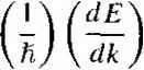 where the у,- in the summation is the associated with the empty state. Equation (3.52) is entirely equivalent to placing a positively charged particle in the empty states and assuming all other states in the band are empty, or neutrally charged. This concept is shown in Figure ЗЛ8. Figure 3.18a shows the valence band with the conventional electron-filled states and empty states, while Figure 3.18b shows the new concept of positive charges occupying the original empty states. This concept is consistent with the discussion of the positively charged empty state in the valence band as shown in Figure 3.17. The щ in the summation of Equation (3.52) is related to how well this positively charged particle moves in the semiconductor. Now consider an electron near the top of the allowed energy band shown in Figure 3.16b. The energy near the top of the allowed energy band may again be approximated by a parabola so that we may write {E - E,) = -C.{k)- (3.53) The energy E. is the energy at the top of the energy band. Since E < for electrons in this band, then the parameter Cj must be a positive quantity. Taking the second derivative of E with respect to k from Equation (3.53), we obtain We may rearrange this equation so that 1 dE ¥~dk (3.54) (3.55)  о о о о о о Figure ЗЛ8 ((а) Valence hand with conventional electron-filled states and empty states, (b) Concept of positive charges occupying the original empty states. (3.56) where m* is again an effective mass. We have argued that C2 is a positive quantity,] which now implies that m* is a negative quantity. An electron moving near the top ol an allowed energy band behaves as if it has a negative mass. We must keep in mind that the effective mass parameter is used to relate quan-j tum mechanics and classical mechanics. The attempt to relate these two theories j leads to this strange result of a negative effective mass. However, we must recall that solutions to Schrodingers wave equation also led to results that contradicted classical mechanics. The negative effective mass is another such example. Tn discussing the concept of effective mass in the last section, we used an analogy j of marbles moving through two liquids. Now consider placing an ice cube in the center of a container filled with water: the ice cube will move upward toward the surface in a direction opposite to the gravitational force. The ice cube appears to have a negative effective mass since its acceleration is opposite to the external force. The effective mass parameter takes into account all internal forces acting on the particle. If we again consider an electron near the top of an allowed energy band and use Newton*s force equation for an applied electric field, we will have Fmb = -eE (3.57) However, m* is now a negative quantity, so we may write -eE -\-eE a--; - (3.58) - m*j m* An electron moving near the top of an allowed energy band moves in the same direction as the applied electric field. The net motion of electrons in a nearly full band can be described by considering just the empty states, provided that a positive electronic charge is associated with each state and that the negative of m* from Equation (3.56) is associated with each state. We now can model this band as having particles with a positive electronic charge and a positive effective mass. The density of these particles in the valence, band is the same as the density of empty electronic energy states. This new particle is the hole. The hole, then, has a positive effective mass denoted by m* and a posi- tive electronic charge, so it will move in the same direction as an applied field. 3*2*5 Metals, Insulators, and Semiconductors Each crystal has its own energy-band structure. We noted that the splitting of the energy states in silicon, for example, to form the valence and conduction bands, was complex. Complex band splitting occurs in other crystals, leading to large variations in band structures between various solids and to a wide range of electrical characteristics observed in these various materials. We can qualitatively begin to understand Comparing Equation (3.55) witii Equation (3,41), we may write 1 dE -2C2 1 7f ~ h? ~ ftf 1 ... 5 6 7 8 9 10 11 ... 55 |
|
© 2026 AutoElektrix.ru
Частичное копирование материалов разрешено при условии активной ссылки |