 |
 |
 |
| Главная Журналы Популярное Audi - почему их так назвали? Как появилась марка Bmw? Откуда появился Lexus? Достижения и устремления Mercedes-Benz Первые модели Chevrolet Электромобиль Nissan Leaf |
Главная » Журналы » Simple coaxial reflectometer 1 ... 15 16 17 18 19 20 21 ... 80 HANDBOOK Receiver Alignment 181 Emin. Emax,     CARRIER WAVE PATTERN Figure 26 Figure 27 Figure 28 (LESS THAN 100% JvlODULATION) 000% MODULATION) (OVER MODULATION) The Resonance To present a resonance curve Curve on the on the Screen, a frequency-Screen modulated signal source must be available. This signal source is a signal generator whose output is the fundamental i-f frequency which is frequency-modulated 5 to 10 kc. each side of the fundamental frequency. A signal generator of this type generally takes the form of an ordinary signal generator with a rotating motor driven tuned circuit capacitor, called a wob- 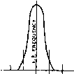 Figure 29 FREQUENCY RESPONSE CURVE OF THE I.F OF A LOW PRICED RECEIVER bulatoT, or its electronic equivalent, a reactance tube. The method of presenting a resonance curve on the screen is to connect the vertical channel of the oscilloscope across the detector load of the receiver as shown in the detectors of figure 31 (between point A and ground) and the time-base generator output to the horizontal channel. In this way the d-c voltage across the detector load varies with the frequencies which are passed by the i-f system. Thus, if the time-base generator is set at the frequency of rotation of the motor driven capacitor, or the reactance tube, a pattern resembling figure 32, a double resonance curve, appears on the screen. Figure 32 is eзфlained by considering figure 33. In half a rotation of the motor driven capacitor the frequency increases from 445 kc. to 465 kc, more than covering the range of frequencies passed by the i-f system. Therefore, a full resonance curve is presented on the screen during this half cycle of rotation since only half a cycle of the voltage producing horizontal deflection has transpired. In the second half of the rotation the motor Figure 30 FREQUENCY RESPONSE OF HIGH-FIDELITY I-F SYSTEM , to audio amp, (to audio [amp. TRIODE DETECTOR DIODE DETECTOR Figure 31 CONNECTION OF THE OSCILLOSCOPE ACROSS THE DETECTOR LOAD 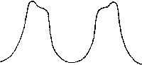 Figure 32 DOUBLE RESONANCE CURVE
Figure 33 DOUBLE RESONANCE ACHIEVED BY COMPLETE ROTATION OF THE MOTOR DRIVEN CAPACITOR 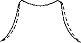 Figure 34 SUPER-POSITION OF RESONANCE CURVES curve is observed as it sweeps the spot across the screen from left to right; audit is observed again as the sine wave sweeps the spot back again from right to left. Under these conditions the two response curves are superimposed on each other and the high frequency responses of both curves are at one end and the low frequency response of both curves is at the other end. The i-f trimmer capacitors are adjusted to produce a response curve which is symmetrical on each side of the fundamental frequency. When using sawtooth sweep, the two response curves can also be superimposed. If the sawtooth signal is generated at exactly twice the frequency of rotation of the motor driven capacitor, the two resonance curves will be superimposed (figure 34) if the i-f transformers are properly tuned. If the two curves do not coincide the i-f trimmer capacitors should be adjusted. At the point of coincidence the tuning is correct. It should be pointed out that rarely do the two curves agree perfectly. As a result, optimum adjustment is made by making the peaks coincide. This latter procedure is the one generally used in i-f adjustment. When the two curves coincide, it is evident that the i-f system responds equally to signals higher and lower than the fundamental i-f frequency. 9-6 Single Sideband Applications Measurement of power output and distortion are of particular importance in SSB transmitter adjustment. These measurements are related to the extent that distortion rises rapidly when the power amplifier is overloaded. The useable power output of a SSB transmitter is often defined as the maximum peak envelope power driven capacitor takes the frequency of the signal in the reverse order through the range of frequencies passed by the i-f system. In this interval the time-base generator sawtooth waveform completes its cycle, drawing the electron beam further across the screen and then returning it to the starting point. Subsequent cycles of the motor driven capacitor and the sawtooth voltage merely retrace the same pattern. Since the signal being viewed is applied through the vertical amplifier, the sweep can be synchronized internally. Some signal generators, particularly those employing a reactance tube, provide a sweep output in the form of a sine wave which is synchronized to the frequency with which the reactance tube is swinging the fundamental frequency through its limits, usually 60 cycles per second. If such a signal is used for horizontal deflection, it is already synchronized. Since this signal is a sine wave, the response   ® ® Figure 35 SINGLE TONE PRESENTATION Osc /oscope trace of SSB signal modulated by single tone (A). Incomplete carrier supress/on or spurious products will show modulated envelope of (B). The ratio of supression is: S = 20 log A+S A-B 5207�97601 HANDBOOK S.S.B. Applications 183 INPUT ENVELOPE DETECTOR POWER AMPLIFIER UNDER TEST OSCILLOSCOPE OUTPUT ENVELOPE DETECTOR GERMANIUM Z.SMH R-F SSB INPUT DIODE RFC divider OR pickup COI L <52.5MH RFC 01 470[ Г to S SCILLOSCOPE Figure 37 SCHEMATIC OF ENVELOPE DETECTOR Figure 36 BLOCK DIAGRAM OF LINEARITY TRACER obtainable with a specified signal-to-distortion ratio. The oscilloscope is a useful instrument for measuring and studying distortion of all types that may be generated in single sideband equipment. Single Tone When a SSB transmitter is modu-Observations lated with a single audio tone, the r-f output should be a single radio frequency. If the vertical plates of the oscilloscope are coupled to the output of the transmitter, and the horizontal amplifier sweep is set to a slow rate, the scope presentation will be as shown in figure 35. If unwanted distortion products or carrier are present, the top and bottom of the pattern will develop a ripple proportional to the degree of spurious products. The Linearity The linearity tracer is an aux-Trocer iliary detector to be used with an oscilloscope for quick observation of amplifier adjustments and parameter variations. This instrument consists of two SSB envelope detectors the outputs of which connect to the horizontal and vertical inputs of an oscilloscope. Figure 36 shows a block diagram of atypical linearity test set-up. A two-tone test signal is normally employed to supply a SSB modulation envelope, but any modulating signal that provides an envelope that varies from zero to full amplitude may be used. Speech modulation gives a satisfactory trace, so that this instrument may be used as a visual monitor of transmitter linearity. It is particularly useful for monitoring the signal level and clearly shows when the amplifier under observation is overloaded. The linearity trace will be a straight line regardless of the envelope shape if the amplifier has no distortion. Overloading causes a sharp break in the linearity curve. Distortion due to too much bias is also easily observed and the adjustment for low distortion can easily be made. Another feature of the linearity detector is that the distortion of each individual stage can be observed. This is helpful in troubleshooting. By connecting the input envelope detector to the output of the SSB generator, the overall distortion of the entire r-f circuit beyond this point is observed. The unit can also serve as a voltage indicator which is useful in making tuning adjustments. The circuit of a typical envelope detector is shown in figure 37. Two matched germainum diodes are used as detectors. The detectors are not linear at low signal levels, but if the nonlinearity of the two detectors is matched, the effect of their nonlinearity on the oscilloscope trace is cancelled. The effect of diode differences is minimized by using a diode load of 5,000 to 10,000 ohms, as shown. It is important that both detectors operate at approximately the same signal level so that their differences will cancel more exactly. The operating level should be 1-volt or higher. It is convenient to build the detector in a small shielded enclosure such as an i-f transformer can fitted with coaxial input and output connectors. Voltage dividers can be similarly constructed so that it is easy to insert the desired amount of voltage attenuation from the various sources. In some cases it is convenient to use a pickup loop on the end of a short length of coaxial cable. The phase shift of the amplifiers in the oscilloscope should be the same and their frequency response should be flat out to at least twenty times the frequency difference of the twotest tones. Excellent high frequency characteristics are necessary because the rectified SSB envelope contains harmonics extending tothe limit of the envelope detectors response. Inadequate frequency response of the vertical amplifier may cause a little foot to appear on the lower end of the trace, as shown in figure 38. If it is small, it may be safely neglected. Another spurious effect often encountered is a double trace, as shown in figure 39- This can usually be corrected with an R-C network placed between one detector and the oscilloscope. The best method of testing the detectors and the amplifiers is to connect the input of 184 The Oscilloscope  Figure 38 EFFECT OF INADEQUATE RESPONSE OF VERTICAL AMPLIFIER  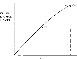 NPUT SIGNAL LEVEL Figure 41 ORDINATES ON LINEARITY CURVE FOR 3RD ORDER DISTORTION EQUATION Figure 39 DOUBLE TRACE CAUSED BY PHASE SHIFT the envelope detectors in parallel. Л perfectly straight line trace will result when everything is working properly. One detector is then connected to tlie other r-f source through a voltage divider adjusted so that no appreciable change in the setting of the oscilloscope amplifier controls is requited. Figure 40 illustrates some typical linearity traces. Trace A is caused by inadequate static plate current in class A or class В amplifiers or a mixer stage. To regain linearity, the grid bias of the stage should be reduced, the screen voltage should be raised, or the signal level should be decreased. Trace В is a result of poor grid circuit regulation when grid current is drawn, or a result of non- linear plate characteristics of the amplifier tube at large plate swings. More grid swamping should be used, or the exciting signal should be reduced. A combination of the effects of A and В are shown in Tr ce C. Trace D illustrates amplifier overloading. The exciting signal should be reduced. A means of estimating the distortion level observed is quite useful. The first and third order distortion components may be derived by an equation that will give the approximate signal-to-distortion level ratio of a two tone test signal, operating on agiven linearity curve. Figure 41 shows a linearity curve with two otdinates erected at hal and full peak input signal level. The length of the ordinates ei and e2 may be scaled and used in the following equation: Signal-to-distortion ratio in db = 20 log 8 ei-e2 2 ei-e2   ®   ® TYPICAL LINEARITY TRACES Figure 40 TYPICAL LINEARITY TRACES CHAPTER TEN Special Vacuum Tube Circuits A whole new concept of vacuum tube applications has been developed in recent years. No longer are vacuum tubes chained to the field of communication. This chapter is devoted to some of the more common circuits encountered in industrial and military applications of the vacuum tube. 10-1 Limiting Circuits The term limiting refers to the removal or suppression by electronic means of the extremities of an electronic signal. Circuits which perform this function are referred to as limiters or clippers. Limiters are useful in wave-shaping circuits where it is desirable to square off the extremities of the applied signal. A sine wave may be applied to a limiter circuit to produce a rectangular wave. A peaked wave may be applied to a limiter circuit to eliminate either the positive or negative peaks from the output. Limiter circuits are employed in FM receivers where it is necessary to limit the amplitude of the signal applied to the detector. Limiters may be used to reduce automobile ignition noise in short-wave receivers, or to maintain a high average level of modulation in a transmitter. They may also be used as protective devices to limit input signals to special circuits. Diode Limiters The characteristics of a diode tube are such that the tube conducts only when the plate is at a positive potential with respect to the cathode. A positive potential may be placed on the cathode, but the tube will not conduct until the voltage on the plate rises above an equally positive value. As the plate becomes more positive with respect to the cathode, the diode conducts and passes that portion of the wave that is more positive than the cathode voltage. Diodes may be used as either series or parallel limiters, as shown in figure I. A diode may be so biased that only a certain portion of the positive or negative cycle is removed. Audio Peak An audio peak clipper consisting Limiting of two diode limiters may be used to limit the amplitude of an audio signal to a predetermined value to provide a high average level of modulation without danger of overmodulation. An effective limiter for this service is the series-diode gate clipper. A circuit of this clipper is shown in figure 2. The audio signal to be clipped is coupled to the clipper through Cj. Rj and Rj are the clipper input and output load resistors. The clipper plates are tied together and are connected to the clipping level control, R through the series resistor, Rj. acts as a voltage divider between the high voltage supply and ground. The exact point at which clip- ® eouT eouT Aftr eouT E = voltage drop across diode eiN- Pout E = VOLTAGE DROP ACROSS DIODE eiN-
eouT e out 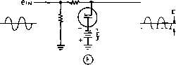 eiN- eouT eiN- -vw- ® - eouT ->j Jt Figure 1 VARIOUS DIODE LIMITING CIRCUITS Series diodes limiting positive and negative peaks are shown in A and B. Parallel diodes limiting positive and negative peaks are shown in С and D. Parallel diodes limiting above and below ground ate shown in E and F. Parallel diode limiters which pass negative ar>d positive peaks are shown in G and H. ping will occur is set by R, which controls the positive potential applied to the diode plates. Under static conditions, a d-c voltage is obtained from R4 and applied through R, to both plates of the 6AL5 tube. Current flows through R4, R3, and divides through the two diode sections of the 6AL5 and the two load resistors, Rl and Rj. All parts of the clipper circuit are maintained at a positive potential above ground. The voltage drop between the plate and cathode of each diode is very small compared to the drop across the 300,000-ohm resistor (Rj) in series with the diode plates. The plate and cathode of each diode are therefore maintained at approximately equal potentials as long as there is plate current flow. Clipping does not occur until the peak audio input voltage reaches a value greater than the static voltages at the plates of the diode. Assume that R4 has been set to a point that will give 4 volts at the plates of the 6AL5. When the peak audio input voltage is less than 4 volts, both halves of the tube conduct at all times. As long as the tube conducts, its resistance is very low compared with the plate resistor Rj. Whenever a voltage change occurs across input resistor R, the voltage at all of the tube elements increases or decreases by the same amount as the input voltage change, and the voltage drop across R3 changes by an equal amount. As long as the peak input voltage is less than 4 volts, the 6AL5 acts merely as a conductor, and the ouфut cathode is permitted to follow all voltage changes at the input cathode. If, under static conditions, 4 volts appear at the diode plates, then twice this voltage (8 volts) will appear if one of the diode circuits HANDBOOK Clamping Circuits 187 6AL5-- 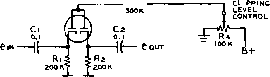 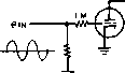 E=GRrD-CATHO0£ RESISTANCE WHEM GRID IS DRIVEN POSITIVE Figure 2 THE SERIES-DIODE GATE CLIPPER FOR AUDIO PEAK LiMITiNG Figure 3 GRID LIMITING CIRCUIT is opened, removing its d-c load from the circuit. As long as only one of the diodes continues to conduct, the voltage at the diode plates cannot rise above twice the voltage selected by R4. In this example, the voltage cannot rise above 8 volts. Now, if the input audio voltage applied through Ci is increased to any peak value between zero and plus 4 volts, the first cathode of the 6AL5 will increase in voltage by the same amount to the proper value between 4 and 8 volts. The other tube elements will assume the same potential as the first cathode. However, the 6AL5 plates cannot increase more than 4 volts above their original 4-volt static level. When the input voltage to the first cathode of the 6AL5 increases to more than plus 4 volts, the cathode potential increases to more than 8 volts. Since the plate circuit potential remains at 8 volts, the first diode section ceases to conduct until the input voltage across R, drops below 4 volts. When the input voltage swings in a negative direction, it will subtract from the 4-volt drop across R, and decrease the voltage on the input cathode by an amount equal to the input voltage. The plates and the ouфut cathode will follow the voltage level at the input cathode as long as the input voltage does not swing below minus 4 volts. If the input voltage does not change more than 4 volts in a negative direction, the plates of the 6AL5 will also become negative. The potential at the output cathode will follow the input cathode voltage and decrease from itsi normal value of 4 volts until it reaches zero potential. As the input cathode voltage decreases to less than zero, the plates will follow. Howe.ver, the ouфut cathode, grounded through Rj, will stop at zero potential as the plate becomes negative. Conduction through the second diode is impossible under these conditions. The ouфut cathode remains at zero potential until the voltage at the input cathode swings back to zero. The voltage developed across ouфut resistor Rj follows the input voltage variations as long as the input voltage does not swing to a peak value greater than the static voltage at the diode plates, determined by R4. Effective clipping may thus be obtained at any desired level. The square-topped audio waves generated by this clipper are high in harmonic content, but these higher order harmonics may be greatly reduced by a low-level speech filter. Grid Limiters A triode grid limiter is shown in figure 3. On positive peaks of the input signal, the triode grid attempts to swing positive, and the grid-cathode resistance drops to a value on the order of 1000 ohms or so. The voltage drop across R (usually of the order of 1 megohm) is large compared to the grid-cathode drop, and the resulting limiting action removes the top part of the positive input wave. 10-2 Clamping Circuits A circuit which holds either amplitude extreme of a waveform to a given reference level eouT 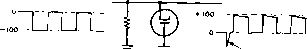 ei.-If DIODE CONDUCTS eouT ® POSITIVE CLAMPING CIRCUIT ® NEGATIVE CLAMPING CIRCUIT Figure 4 SIMPLE POSITIVE AND NEGATIVE CLAMPING CIRCUITS eiN- - -roov. OEFLECTrON COrL 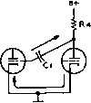 Cr CHARGE PATH  Сг DISCHARGE PATH Figure 5 NEGATIVE CLAMPING CIRCUIT EM-PLOYED IN ELECTROMAGNETIC SWEEP SYSTEM Figure 7 THE CHARGE AND DISCHARGE PATHS IN FREE-RUNNING MULTIVIBRATOR OF FIGURE 6 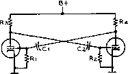 Figure 6 BASIC MULTIVIBRATOR CIRCUIT of potential is called a clamping circuit or a d-c restorer. Clamping circuits are used after RC cpupling circuits where the waveform swing is required to be either above or below the reference voltage, instead of alternating on both sides of it (figure 4). Clamping circuits are usually encountered in oscilloscope sweep circuits. If the sweep voltage does not always start from the same reference point, the trace on the screen does not begin at the same point on the screen each time the sweep is repeated and therefore is jittery. If a clamping circuit is placed between the sweep amplifier and the deflection element, the start of the sweep can be regulated by adjusting the d-c voltage applied to the clamping tube (figure 5). 10-3 Multivibrators The multivibrator, or relaxation oscillator, is used for the generation of nonsinusoidal waveforms. The output is rich in harmonics, but the inherent frequency stability is poor. The multivibrator may be stabilized by the introduction of synchronizing voltages of harmonic or subharmonic frequency. In its simplest form, the multivibrator is a simple two-stage resistance-capacitance coupled amplifier with the оифиг of the second stage coupled through a capacitor to the grid of the first tube, as shown in figure 6. Since the оифиг of the second stage is of the proper polarity to reinforce the input signal applied to the first tube, oscillations can readily take place, started by thermal agitation noise and 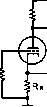 ® DIRECT-COUPLED CATHODE MULTIVIBRATOR 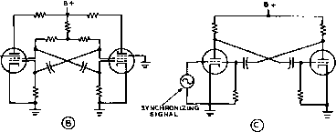 ELECTRON-COUPLED MULTIVIBRATOR MULTIVIBRATOR WITH SINE-WAVE SYNCHRONIZING SIGNAL APPLIED TO ONE TUBE Figure 8 VARIOUS FORMS OF MULTIVIBRATOR CIRCUITS HANDBOOK Multivibrators ]89 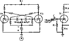 PULSE Vi Output BASIC ECCLES-JORDAN TRIGGER CIRCUIT ONE-SHOT MULTIVIBRATOR Figure 9 ECCLES-JORDAN MULTIVIBRATOR CIRCUITS miscellaneous tube noise. Oscillation is maintained by the process of building up and discharging the store of energy in the grid coupling capacitors of the two tubes. The charging and discharging paths are shown in figure 7. Various forms of multivibrators are shown in figure 8. The ouфut of a multivibrator may be used as a source of square waves, as an electronic switch, or as a means of obtaining frequency division. Submultiple frequencies as low as one-tenth of the injected synchronizing frequency may easily be obtained. The Eccles-Jordan The Eccles-Jordan trigger Circuit circuit is shown in figure 9A. This is not a true multivibrator, but rather a circuit that possesses two conditions of stable equilibrium. One condition is when Vi is conducting and V is cutoff; the other when Vj is conducting and V, is cutoff. The circuit remains in one or the other of these two stable conditions with no change in operating potentials until some external action occurs which causes the nonconducting tube to conduct. The tubes then reverse their functions and remain in the new condition as . long as no plate current flows in the cutoff tube. This type of circuit is known as a jlip-flop circuit. 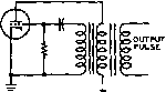 eooT HiSiNG f\j \ Figure 9B illustrates a modified Eccles-Jotdan circuit which accomplishes a complete cycle when triggered with a positive pulse. Such a circuit is called a one-shot multivibrator. For initial action, V, is cutoff and Vj is conducting. A large positive pulse applied to the grid of V, causes this tube to conduct, and the voltage at its plate decreases by virtue of the IR drop through Rj. Capacitor Cj is charged rapidly by this abrupt change in Vi plate voltage, and Vj becomes cutoff while Vj conducts. This condition exists until Cj discharges, allowing Vj to conduct, raising the cathode bias of Vi until it is once again cutoff. A direct, cathode-coupled multivibrator is shown in figure 8A. R is a common cathode resistor for the two tubes, and coupling takes place across this resistor. It is impossible for a tube in this circuit to completely cutoff the other tube, and a circuit of this type is called a free-running multivibrator in which the condition of one tube temporarily cuts off the other. 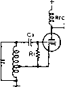 rf PULSE RF PULSE PULSE He- % % CUTOFF TIME cutoff time Figure 11 Figure 10 SINGLE-SWING BLOCKING OSCILLATOR HARTLEY OSCILLATOR USED AS BLOCKING OSCILLATOR BY PROPER CHOICE OF R-Ci e.NH(- -eouT em- -eouT  ® POSITIVE COUNTING CIRCUIT © NEGATIVE COUNTING CIRCUIT POSITIVE COUNTING CIRCUIT WITH METER INDICATION Figure 12 POSITIVE AND NEGATIVE COUNTING CIRCUITS 10-4 The Blocking Oscillator A blocking oscillator is any oscillator which cuts itself off after one or more cycles caused by the accumulation of a negative charge on the grid capacitor. This negative charge may gradually be drained off through the grid resistor of the tube, allowing the circuit to oscillate once again. The process is repeated and the tube becomes an intermittent oscillator. The rate of such an occurance is determined by the R-C time constant of the grid circuit. A single-swing blocking oscillator is shown in figure 10, wherein the tube is cutoff before the completion of one cycle. The tube produces single pulses of energy, the time between the pulses being regulated by the discharge time of the grid R-C network. The self-pulsing blocking oscillator is shown in figure 11, and is used to produce pulses of r-f energy, the number of pulses being determined by the timing network in the grid circuit of the oscillator. The rate at which these pulses occur is known as the pulse-repetition frequency, or p.r.f. ing units to be counted, and produces a voltage that is proportional to the frequency of the pulses. A counting circuit may be used in conjunction with a blocking oscillator to produce a trigger pulse which is a submultiple of of the frequency of the applied pulse. Either positive or negative pulses may be counted. A positive counting circuit is shown in figure 12A, and a negative counting circuit is shown in figure 12B. The positive counter allows a certain amount of current to flow through R each time a pulse is applied to Ci. The positive pulse charges C and makes the plate of Vj positive with respect to its cathode. Vj conducts until the exciting pulse passes. Cl is then discharged by Vi, and the circuit is ready to accept another pulse. The average current flowing through Ri increases as the pulse-repetition frequency increases, and decreases as the p.r.f. decreases. By reversing the diode connections, as shown in figure 12B, the circuit is made to respond to negative pulses. In this circuit, an increase in the p.r.f. causes a decrease in the average current flowing through Ri, which is opposite to the effect in the positive counter. 10-5 Counting Circuits A counting circuit, or frequency divider is one which receives uniform pulses, represent- ee in-HH--p-@Lr-e out.  Figure 13 STEP-BY-STEP COUNTING CIRCUIT em-HI- о о о о оеоит о о Figure 14 The step-bystep caunfer used to trigger a blocking oselllafor. The blocking oscillator serves as a frequency diyider. 1 ... 15 16 17 18 19 20 21 ... 80 |
||||||||||||||||||||||
|
© 2026 AutoElektrix.ru
Частичное копирование материалов разрешено при условии активной ссылки |