 |
 |
 |
| Главная Журналы Популярное Audi - почему их так назвали? Как появилась марка Bmw? Откуда появился Lexus? Достижения и устремления Mercedes-Benz Первые модели Chevrolet Электромобиль Nissan Leaf |
Главная » Журналы » Simple coaxial reflectometer 1 ... 30 31 32 33 34 35 36 ... 80 in amplitude modulation is of no practical value in SSB because the SSB r-f envelopes are so different than the audio envelopes. A heavily clipped wave approaches a square wave and a square wave gives a SSB envelope with peaks of infinite amplitude as shown in figure 7B. Carrier Frequency Stability Requirements Reception of a SSB signal is accomplished by simply heterodyning the carrier down to zero frequency. (The conversion frequency used in the last heterodyne step is often called the reinserted carrier). If the SSB signal is not heterodyned down to exactly zero frequency, each frequency component of the detected audio signal will be high or low by the amount of this error. An error of 10 to 20 c.p s. for speech signals is acceptable from an intelligibihty standpoint, but an error of the order of 50 c.p.s. seriously degrades the intelligibility. An error of 20 c.p.s. is not acceptable for the transmission of music, however, because the harmonic relationship of the notes would be destroyed. For example, the harmonics of 220 c.p.s. are 440, 660, 880, etc., but a 10 c.p s. error gives 230, 450, 670, 890, etc., or 210, 430, 650, 870, etc., if the original error is on the other side. This error would destroy the original sound of the tones, and the harmony between the tones. Suppression of the carrier is common in amateur SSB work, so the combined frequency stabilities of all oscillators in both the transmitting and receiving equipment add together to give the frequency error found in detection. In order to overcome much of the frequency stability problem, it is common commercial practice to transmit a pilot carrier at a reduced amplitude. This is usually 20 db below one tone of a two-tone signal, or 26 db below the peak envelope power rating of the transmitter. This pilot carrier is filtered out from the other signals at the receiver and either amplified and used for the reinserted carrier or used to control the frequency of a local oscillator. By this means, the frequency drift of the carrier is eliminated as an error in detection. Advantage of SSB with Selective Fading On long distance communication circuits using a-m, selective fading often causes severe distortion and at times makes the signal unintelligible. When one sideband is weaker than the other, distor-  PUSH-PULL AUDIO IN Figure 8 SHOWING TWO COMMON TYPES OF BALANCED MODULATORS Notice that a balanced modulator changes the circuit condition from single ended to push-pull, or vice versa. Choice of circuit depends upon external circuit conditions since both the (A) and (B) arrangements can give satisfactory generation of a double-sideband suppressed-carrier signal. tion results; but when the carrier becomes weak and the sidebands are strong, the distortion is extremely severe and the signal may sound hke monkey chatter. This is because a carrier of at least twice the amplitude of either sideband is necessary to demodulate the signal properly. This can be overcome by using exalted carrier reception in which the carrier is amplified separately and then reinserted before the signal is demodulated or detected. This is a great help, but the reinserted carrier must be very close to the same phase as the original carrier. For example, if the reinserted carrier were 90 degrees from the original source, the a-m signal would be converted to phase modulation and the usual a-m detector would deliver no output. The phase of the reinserted carrier is of no importance in SSB reception and by using a strong reinserted carrier, exalted carrier reception is in effect realized. Selective fading with one sideband simply changes the amplimde md the frequency response of the system and very seldom causes the signal to become unintelligible. Thus the receiving techniques used with SSB are those which inherently greatly minimize distortion due to selective fading. 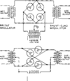 RING MODULATOR DOUBLE-BALANCED -fjJ MODULATOR CARRIER VOLTACE Figure 9 TWO TYPES OF DIODE BALANCED MODULATOR Such balanced modulaior circuits are com-manly used in carrier telephone work and in single-sideband systems where the carrier frequency and modulating frequency are relatively close together. Vacuum diodes, copper-oxide rectifiers, or crystal diodes may be used in the circuits. 17-3 Carrier Elimination Circuits Various circuits may be employed to eliminate the carrier to provide a double sideband signal. A selective filter may follow the carrier elimination circuit to produce a single sideband signal. Two modulated amplifiers may be connected with the carrier inputs 180° out of phase, and with the carrier outputs in parallel. The car- rier will be balanced out of the output circuit, leaving only the two sidebands. Such a circuit is called a balanced modulator. Any non-linear element will produce modulation. That is, if two signals are put in, sum and difference frequencies as well as the original frequencies appear in the output. This phenomenon is objectionable in amplifiers and desirable in modulators or mixers. In addition to the sum and difference frequencies, other outputs (such as twice one frequency plus the other) may appear. All combinations of all harmonics of each input frequency may appear, but in general these are of decreasing amplitude with increasing order of harmonic. These outputs are usually rejected by selective circuits following the modulator. All modulators are not alike in the magnitude of these higher order outputs. Balanced diode rings operating in the square law region are fairly good and pentagrid converters much poorer. Excessive carrier level in tube mixers will increase the relative magnitude of the higher order outputs. Two types of triode balanced modulators are shown in figure 8, and two types of diode modulators in figure 9. Balanced modulators employing vacuum tubes may be made to work very easily to a point. Circuits may be devised wherein both input signals may be applied to a high impedance grid, simplifying isolation and loading problems. The most important difficulties with these vacuum tube modulator circuits are: (1) Balance is not independent of signal level. (2) Balance drifts with time and environment. (3) The carrier level for low high-order output is critical, and (4) Such circuits have limited dynamic range. A number of typical circuits are shown in figure 10. Of the group the most satisfactory performance is to be had from plate modulated triodes. 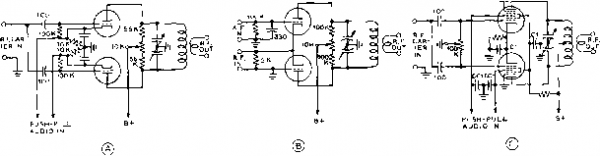 PLATE MODULATED BALANCED TRIODE MODULATOR BALANCED TRIODE MODULATOR WITH SINGLE ENDED INPUT CIRCUITS Figure TO BALANCED MODULATORS BALANCED PENTAGRID CONVERTER MODULATOR  0 о CARRIER VOLTAGE HIGH Z MODULATING VOLTAGE 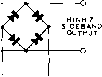 CARRIER VOLTAGE DOUBLE-BALANCED RING MODULATOR SHUNT-QUAD MODULATOR Figure 11 DIODE RING MODULATORS 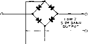 LOW Z MODULATING VOLTAGE о CARRIER VOLTAGE SERIES-QUAD MODULATOR Diode Ring Modulation in telephone car-Modulators rier equipment has been very successfully accomplished with copper-oxide double balanced ring modulators. More recently, germanium diodes have been applied to similar circuits. The basic diode ring circuits are shown in figure 11. The most widely applied is the double balanced ring (A). Both carrier and input are balanced with respect to the output, which is advantageous when the output frequency is not sufficiently different from the inputs to allow ready separation by filters- It should be noted that the carrier must pass through the balanced input and output transformers. Care must be taken in adapting this circuit to minimize the carrier power that will be lost in these elements. The shunt and series quad circuits are usable when the output frequencies are entirely different (i.e.: audio and r.f.). The shunt quad (B) is used with high source and load impedances and the series quad (C) with low source and load impedances. These two circuits may be adapted to use only two diodes, substituting a balanced transformer for one side of the bridge, as shown in figure 12. It should be noted that these circuits present a half-wave load to the carrier source. In applying any of these circuits, r-f chokes and capacitors must be employed to control the path of signal and carrier currents. In the shunt pair, for example, a blocking capacitor is used to prevent the r-f load from shorting the audio input. To a first approximation, the source and load impedances should be an arithmetical mean of the forward and back resistances of the diodes employed. A workable rule of thumb is that the source and load impedances be ten to twenty times the forward resistance for semi-conductor rings. The high frequency limit of operation in the case of junction and copper-oxide diodes may be appreciably extended by the use of very low source and load impedances. Copper-oxide diodes suitable for carrier work are normally manufactured to order. They offer no particular advantage to the amateur, though their excellent long-term stability is important in commercial applications. Rectifier types intended to be used as meter rectifiers are not likely to have the balance or high frequency response desirable in amateur SSB transmitters. Vacuum diodes such as the 6AL5 may be used as modulators. Balancing the heater-cathode capacity is a major difficulty except when the 6AL5 is used at low source and load impedance levels- In addition, contact potentials of the order of a few tenths of a volt may also disturb low level applications (figure 13). The double diode circuits appear attractive, but in general it is more difficult to balance a transformer at carrier frequency than an additional pair of diodes. Balancing potentiometers may be employed, but the actual cause of the unbalance is far more subtile, and cannot be adequately corrected with a single adjustment. A signal produced by any of the above circuits may be classified as a double sideband, suppressed-carrier signal. ® MODULATING VOLTAGE- SIDEBAND OUTPUT SHUNT-PAIR MODULATOR 1ЯЯЯПГ CARRIER VOLTAGE SERIES-PAIR MODULATOR 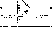 6 0 CARRIER VOLTACE Figure 12 DOUBLE-DIODE PAIRED MODULATORS 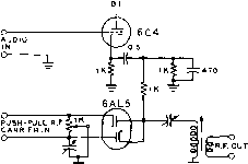 (a) series-balanced diode modulator using 6al5 tube 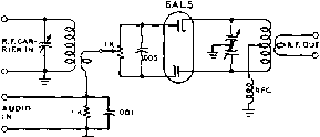 (B) ring-diode modulator using 6AL5 tube Figure 13 VACUUM DIODE MODULATOR CIRCUITS 17-4 Generation of Single-Sideband Signals In general, there are two commonly used methods by which a single-sideband signal may be generated. These systems are: (1) The Filter Method, and (2) The Phasing Method. The systems may be used singly or in combination, and either method, in theory, may be used at the operating frequency of the transmitter or at some other frequency with the signal at the operating frequency being obtained through the use of frequency changers (mixers). The Filter The filter method for obtaining Method a SSB signal is the classic meth- od which has been in use by the telephone companies for many years both for о
-e -s -4 -3 -г -1 о +1 kilocycles deviation Figure 15 BANDPASS CHARACTERISTIC OF BURNELL S-15000 SINGLE SIDEBAND FILTER land-line and radio communications. The mode of operation of the filter method is diagrammed in figure 14, in terms of components and filters which normally would be available to the amateur or experimenter. The output of the speech amplifier passes through a conventional speech filter to limit the frequency range of the speech to about 200 to 3000 cycles. This signal then is fed to a balanced modulator along with a 50,000-cycle first carrier from a self-excited oscillator. A low-frequency balanced modulator of this type most conveniently may be made up of four diodes of the vacuum or crystal type cross connected in a balanced bridge or ring modulator circuit. Such a modulator passes only the sideband components resulting from the sum and difference between the two signals being fed to the balanced modulator. The audio signal and the 50-kc. carrier signal from the oscillator both cancel out in the balanced modulator so that a band of frequencies between 47 and 50 kc. and another band of frequencies between 50 and 53 kc. appear in the output. The signals from the first balanced modulator are then fed through the most critical wo-100001 4T-50KC. so RC. OSCILLATOR
irSO-1950 KC. OSCILLATOR HIGH-Q TUNEDCIRCUIT FOR OUTPUT IN l 00-aOOOKC.BAND Figure 14 BLOCK DIAGRAM OF FILTER EXCITER EMPLOYING A 50-K.C. SIDEBAND FILTER 6AU6 I2AU7 6AL5 -laAU? SHUNT-DIODE imODULATOK K.F. AMPLIFIER .Ot 0.1 7 MH 250jLIUF 6C4 PHASe-INVERfTER 01  PUSH-PULL R.F. TO BALANCED MODULATOR FOR CONVERSION TO leo METERS Wyr: UNLESS OTHERWISE SPECIFIED; RESISTORS ARE O.S WATT. CAPACITORS IN jjf. Figure 16 OPERATIONAL CIRCUIT FOR SSB EXCITER USING THE BURNELL 50-KC. SIDEBAND FILTER component in tiie whole system-the first sideband filter. It is the function of this first sideband filter to separate the desired 47 to 50 kc. sideband from the unneeded and undesired 50 to 53 kc. sideband. Hence this filter must have low attenuation in the region between 47 and 50 kc, a very rapid slope in the vicinity of 50 kc, and a very high attenuation to the sideband components falling between 50 and 53 kilocycles. Burnell & Co., Inc., of Yonkers, New York produce such a filter, designated as Burnell S-15,ООО. The passband of this filter is shown in figure 15. Appearing, then, at the output of the filter is a single sideband of 47 kc. to 50 kc. This sideband may be passed through a phase inverter to obtain a balanced output, and then fed to a balanced mixer. A local oscillator operating in the range of 1750 kc to 1950 kc is used as the conversion oscillator. Additional conversion stages may now be added to trans- late the SSB signal to the desired frequency. Since only linear amplification may be used, it is not possible to use frequency multiplying stages. Any frequency changing must be done by the beating-oscillator technique. An operational circuit of this type of SSB exciter is shown in figure 16. A second type of filter-exciter for SSB may be built around the Collins Mechanical Filter. Such an exciter is diagrammed in figure 17. Voice frequencies in the range of 200-3000 cycles are amplified and fed to a low impedance phase-inverter to furnish balanced audio. This audio, together with a suitably chosen r-f signal, is mixed in a ring modulator, made up of small germanium diodes. Depending upon the choice of frequency of the r-f oscillator, either the upper or lower sideband may be applied to the input of the mechanical filter. The carrier, to some extent, has been rejected by the ring modulator. Additional carrier rejection is afforded by the excellent passband гоо-зооо 1 гоо-зооо ъ 4S3-4SeKC. SPEECH AMPLIFIER LOW Z PHASE INVERTER 453-4 seKC. SHUNT-QUAD RIN MODULATOR 4SiK.C. MECHANICAL FILTER CONVERTER 4S0-453KC. S3 K.C. OSCILLATOR 3S00 K.C. OSCILLATOR R.F. AMPLIFIER WITH HICH-Q TUNED CIRCUIT FOR OUTPUT ON 3953 KC. Figure 17 BLOCK DIAGRAM OF FILTER EXCITER EMPLOYING A 455-KC. MECHANICAL FILTER FOR SIDEBAND SELECTION 336 Sideband Transnnission THE RADIO l,r.TRAN3 LF. TRANS. 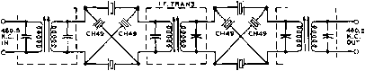 FT-24I CHAHHEL 49 CnySTAL 4ei. I KC. FT-!4I CHANNEL 50 CRySTAL = 4вг.ЯКС. Figure 18 SIMPLE CRYSTAL LATTICE FILTER ш z о э z ш 1-I- < I
4S9 4вО 461 462 4ез 464 frequency (кс.) characteristics of the mechanical filter. For simplicity, the mixing and filtering operation usually takes place at a frequency of 455 kilocycles. The single-sideband signal appearing at the output of the mechanical filter may be translated directly to a higher operating frequency. Suitable tuned circuits must follow the conversion stage to eliminate the signal from the conversion oscillator. Wove Filters The heart of a filter-type SSB exciter is the sideband filter. Conventional coils and capacitors may be used to construct a filter based upon standard wave filter techniques. The Q of the filter inductances must be high when compared with the reciprocal of the fractional bandwidth. If a bandwidth of 3 kc. is needed at a carrier frequency of 50 kc, the bandwidth expressed in terms of the carrier frequency is 3/50 or 6%. This is expressed in terms of fractional bandwidth as 1/16. For satisfactory operation, the ш Q 20 о - 30 < Z 40 ш
246 247 248 249 2S0 251 252 2ЬЗ 254 FREQUENCY (K.C.) Figure 19 PASSBAND OF LOWER AND UPPER SIDEBAND MECHANICAL FILTER Q of the filter inductances should be 10 times the reciprocal of this, or 160. Appropriate Q is generally obtained from toroidal inductances, though there is some possibility of using iron core solenoids between 10 kc. and 20 kc. A characteristic impedance below 1000 ohms should be selected to prevent distributed capacity of the inductances from spoiling overall performance. Paper capacitors intended for bypass work may not be trusted for stability or low loss and should not be used in filter circuits. Care should be taken that the levels of both accepted and rejected signals are low enough so that saturation of the filter inductances does not occur. Crystal Filters The best known filter responses have been obtained with crystal filters. Types designed for program carrier service cut-off 80 db in less than 50 cycles. More than 80 crystals are used in this type of filter. The crystals are cut to control reactance and resistance as well as the resonant frequency. The circuits used are based on full lattices. The war-surplus low frequency crystals may be adapted to this type of filter with some success. Experimental designs usually synthesize a selectivity curve by grouping sharp notches at the side of the passband. Where the width of the passband is greater than twice the spacing of the series and parallel resonance of the crystals, special circuit techniques must be used. A typical crystal filter using these surplus crystals, and its approximate pass-band is shown in figure 18. Mechanical Filters Filters using mechanical resonators have been studied by a number of companies and are offered commercially by the Collins Radio Co. They are available in a variety of bandwidths
200-3000 AUDIO PHASE SPLITTING NETWORKS PHASe difper£nc€ between St and 2 = 90 phase difference between 1 and 2 = 90 BALANCED MODULATOR MODULATOHl- RADIO FREQ. PHASE SPLITTING NETWORK RADIO FREQ. SIGNAL AT CARRIER FREQ. TO POWER AMPLIFIER STAGES OH DIRECTLY TO ANTENNA SYSTEM Figure 20 BLOCK DIAGRAM OF THE PHASING METHOD The phasing method of obtaining a single-sideband signal is simpler than the filter system in regard to the number of tubes and circuits required. The system is also less expensive In regard to the components required, bat is more critical in regard to adiustments for the transmission of a pure single-sideband signal. at center frequencies of 250 kc. and 455 kc. The 250 kc. series is specifically intended for sideband selection. The selectivity attained by these filters is intermediate between good LC filters at low center frequencies and engineered quartz crystal filters- A passband of two 250 kc. filters is shown in figure 19- In application of the mechanical filters some special precautions are necessary. The driving and pick-up coils should be carefully resonated to the operating frequency. If circuit capacities are unknown, trimmer capacitors should be used across the coils. Maladjustment of these tuned coils will increase insertion loss and the peak-to-valley ratio. On high impedance filters (ten to twenty thousand ohms) signals greater than 2 volts at the input should be avoided. D-c should be blocked out of the end coils. While the filters are rated for 5 ma. of coil current, they are not rated for d-c plate voltage. The Phasing There are a number of points System of view from which the op- eration of the phasing system of SSB generation may be described. We may state that we generate two double-sideband suppressed carrier signals, each in its own balanced modulator, that both the r-f phase and the audio phase of the two signals differ by 90 degrees, and that the outputs of the two balanced modulators are added with the result that one sideband is increased in amplitude and the other one is cancelled. This, of course, is a true description of the action that takes place. But it is much easier to consider the phasing system as a method simply of adding (or of subtracting) the desired modulation frequency and the nominal carrier frequency. The carrier frequency of course is not trans- mitted, as is the case with all SSB transmissions, but only the sum or the difference of the modulation band from the nominal carrier is transmitted (figure 20) - The phasing system has the obvious advantage that all the electrical circuits which give rise to the single sideband can operate in a practical transmitter at the nominal output frequency of the transmiter. That is to say that if we desire to produce a single sideband whose nominal carrier frequency is 3-9 Mc-, the balanced modulators are fed with a З-9-Мс. signal and with the audio signal from the phase splitters. It is not necessary to go through several frequency conversions in order to obtain a sideband at the desired output frequency, as in the case with the filter method of sideband generation. Assuming that we feed a speech signal to the balanced modulators along witti the 3900-kc. carrier (3-9 Mc.) we will obtain in the output of the balanced modulators a signal which is either the sum of the carrier signal and the speech band, or the difference between the carrier and the speech band- Thus if our speech signal covers the band from 200 to 3000 cycles, we will obtain in the output a band of frequencies from 3900.2 to 3903 kc. (the sum of the two, or the upper sideband), or a band from 3897 to 3899.8 kc (the difference between the two or the lower sideband). A further advantage of the phasing system of sideband generation is the fact that it is a very simple matter to select either the upper sideband or the lower sideband for transmission. A simple double-pole double-throw reversing switch in two of the four audio leads to the balanced modulators is all that is required.  0 ie0 90 270 FOUR-PHASE A F. 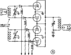 0 teO 90 270 -.-/ FOUR-PHASE A.F. Figure 21 TWO CIRCUITS FOR SINGLE SIDEBAND GENERATION BY THE PHASING METHOD. The circuit of (A) offers the advantages of simplicity in the single-ended input circuits plus a push-pull output circuit. Circuit (B) requires double-ended input circuits but allows all the plates io be connected in parallel tor the output circuit. High-Level Phasing Vs. Low-Level Phasing The piate-circuit efficiency of the four tubes usually used to make up the two balanced modulators of the phasing system may run as high as 50 to 70 per cent, depending upon the operating angle of plate current flow. Hence it is possible to operate the double balanced modulator directly into the antenna system as the output stage of the transmitter. The alternative arrangement is to generate the SSB signal at a lower level and then to amplify this signal to the level desired by means of class A or class В r-f power amplifiers. If the SSB signal is generated at a level of a few milliwatts it is most common to make the first stage in the amplifier chain a class A amplifier, then to use one or more class В linear amplifiers to bring the output up to the desired level. Balanced Modulator Circuits Illustrated in figure 8 are the two basic balanced modulator circuits which give good results with a radio frequency carrier and an audio modulating signal. Note that one push-pull and one single ended tank circuit is required, but that the push-pull circuit may be placed either in the plate or the grid circuit. Also, the audio modulating voltage always is fed into the stage in push-pull, and the tubes normally are operated Class A. When combining two balanced modulators to make up a double balanced modulator as used in the generation of an SSB signal by the phasing system, only one plate circuit is required for the two balanced modulators. However, separate grid circuits are required since the grid circuits of the two balanced modulators operate at an r-f phase difference of 90 degrees. Shown in figure 21 are the two types of double balanced modulator circuits used for generation of an SSB signal. Note that the circuit of figure 21A is derived from the balanced modulator of figure 8A, and similarly figure 2IB is derived from figure 8B. Another circuit that gives excellent performance and is very easy to adjust is shown in figure 22. The adjustments for carrier balance are made by adjusting the potentiometer for voltage balance and then the small variable capacitor for exact phase balance of the balanced carrier voltage feeding the diode modulator. 0.г VOLT MECHANICAL FILTER I 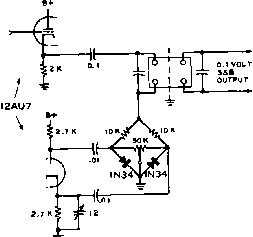 R-F CARRIER , rt: 2,5 VOLTS Figure 22 BALANCED MODULATOR FOR USE WITH MECHANICAL FILTER 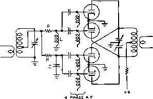 Figure 23 LOW-Q R-F PHASE-SHIFT NETWORK The r-f phase-shift system Illustrated above is convenient in a case where it is desired ta moke smoif changes in the operating frequency of the system without the necessity of being precise in the adiustment of two coupled circuits as used for r-f phase shift in the circuit of figure 21. Radio-Frequency Phasing A single-sideband generator of the phasing type requires that the two balanced modulators be fed with r-f signals having a 90-degree phase difference. This r-f phase difference may be obtained through the use of two loosely coupled resonant circuits, such as illustrated in figures 21A and 2IB. The r-f signal is coupled directly or inductively to one of the tuned circuits, and the coupling between the two circuits is varied until, at resonance of both circuits, the r-f voltages developed across each circuit have the same amplitude and a 90-degree phase difference. The 90-degree r-f phase difference also may be obtained through the use of a low-Q phase shifting network, such as illustrated in figure 23; or it may be obtained through the use of a lumped-constant quarter-wave line. The low-Q phase-shifting system has proved quite practicable for use in single-sideband systems, particularly on the lower frequencies. In such an arrangement the two resistances R have the same value, usually in the range between 100 and a few thousand ohms. Capacitor C, in shunt with the input capacitances of the tubes and circuit capacitances, has a reactance at the operating frequency equal to the value of the resistor R. Also, inductor L has a net inductive reactance equal in value at the operating frequency to resistance R. The inductance chosen for use at L must take Into account the cancelling effect of the input capacitance of the tubes and the circuit capacitance; hence the inductance should be 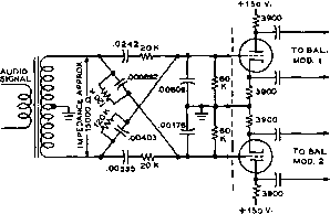 Figure 24 DOME AUDIO-PHASE-SHIFT NETWORK This circuit orrongement is convenient for obtaining the audio phase shift when it is desired to use a minimum af circuit components and tube elements. variable and should have a lower value of inductance than that value of inductance which would have the same reactance as resistor R. Inductor L may be considered as being made up of two values of inductance in parallel; (a) a value of inductance which will resonate at the operating frequency with the circuit and tube capacitances, and (b) the value of inductance which is equal in reactance to the resistance R. In a network such as shown in figure 23, equal and opposite 45-degree phase shifts are provided by the RL and RC circuits, thus providing a 90-degree phase difference between the excitation voltages applied to the two balanced modulators. Audio-Frequency Phasing The audio-frequency phase-shifting networks used in generating a single-sideband signal by the phasing method usually are based on those described by Dome in an article in the December, 1946, Electronics. A relatively simple network for accomplishing the 90-degree phase shift over the range from 160 to 3500 cycles is illustrated in figure 24. The values of resistance and capacitance must be carefully checked to insure minimum deviation from a 90-degree phase shift over the 200 to 3000 cycle range. Another version of the Dome network is shown in figure 25. This network employs three 12AU7 tubes and provides balanced output for the two balanced modulators. As with the previous network, values of the resistances within the network must be held to very close tolerances. It is necessary to restrict the speech range to 300 to 3000 cycles with this network. Audio frequencies outside this range will not have the necessary phase-shift at the output 12AU7 I2AU7 12AU7 I-+105 V. PECULATED  -° - TOBAL MOD 2 -О 4.7k: + 105V. REOULATEO Figure 25 A VERSION OF THE DOME AUDIO-PHASE-SHIFT NETWORK of the network and will show up as spurious emissions on the sideband signal, and also in the region of the rejected sideband. A low-pass 3500 cycle speech filter, such as the Chicago Transformer Co. LPP-2 should be used ahead of this phase-shift network. A passive audio phase-shift network that employs no tubes is shown in figure 26. This network has the same type of operating restrictions as those described above. Additional information concerning phase-shift networks will be found in Single Sideband Techniques published by the Cowan Publishing Corp., New York, and The Single Sideband Digest published by the American Radio Relay League. A comprehensive sideband review is contained in the December, 1956 issue of Proceedings of the 1.R.E Comparison of Filter Either the filter or the and Phasing Methods phasing method of of SSB Generation single-sideband gener- ation is theoretically capable of a high degree of performance. In general, it may be said that a high degree of unwanted signal rejection may be attained with less expense and circuit complexity with the filter method. The selective circuits for rejection of unwanted frequencies operate at a relativly low frequency, are designed for this one frequency and have a relatively high order of Q. Carrier rejection of the order of 50 db or so may be obtained with a relatively simple filter and a balanced modulator, and unwanted sideband rejection in the region of 60 db is economically possible. The phasing method of SSB generation exchanges the problems of high-Q circuits and linear amplification for the problems of accurately controlled phase-shift networks. If the  Figure 26 PASSIVE AUDIO-PHASE-SHIFT NETWORK, USEFUL OVER RANGE OF 300 TO 3000 CYCLES. phasing method is employed on the actual transmitting frequency, change of frequency must be accompanied by a corresponding rebalance of the phasing networks. In addition, it is difficult to obtain a phase balance with ordinary equipment within 2% over a band of audio frequencies. This means that carrier suppression is limited to a maximum of 40 db or so. However, when a relatively simple SSB transmitter is needed for spot frequency operation, a phasing unit will perform in a satisfactory manner. Where a high degree of performance in the SSB exciter is desired, the filter method and the phasing method may be combined. Through the use of the phasing method in the first balanced modulator those undesired sideband components lying within 1000 cycles of the carrier may be given a much higher degree of rejection than is attainable with the filter method alone, with any reasonable amount of complexity in the sideband filter. Then the sideband filter may be used in its normal way to attain very high attenuation of all undesired sideband components lying perhaps further than 500 cycles away from the carrier, and to restrict the sideband width on the desired side of the carrier to the specified frequency limit. 17-5 Single Sideband Frequency Conversion Sysf-ems In many instances the band of sideband frequencies generated by a low level SSB transmitter must be heterodyned up to the desired carrier frequency. In receivers the circuits which perform this function are called converters or mixers. In sideband work they are usually termed mixers or modulators. Mixer Stages One circuit which can be used for this purpose employs a receiving-type mixer tube, such as the 6BE6. The output signal from the SSB generator is fed into the #1 grid and the conversion fre- 1 ... 30 31 32 33 34 35 36 ... 80 |
|||||||||||||||||||||||||||||||||||||||||||||||||||||||||||||||||||||||||||||||||||||||||||||||||||||||||||||||||||||||||||||||||||||||||||||||||||||||||||||||||||||||||||||||||||||||||||||||||||||||||||||||||||||||||||||||||||||||||
|
© 2026 AutoElektrix.ru
Частичное копирование материалов разрешено при условии активной ссылки |