 |
 |
 |
| Главная Журналы Популярное Audi - почему их так назвали? Как появилась марка Bmw? Откуда появился Lexus? Достижения и устремления Mercedes-Benz Первые модели Chevrolet Электромобиль Nissan Leaf |
Главная » Журналы » Simple coaxial reflectometer 1 ... 53 54 55 56 57 58 59 ... 80 r-f, mixer, and oscillator stages. Series padding in the r-f and mixer circuits is employed for good tracking across the band. An i-f channel of 1.5 Mc. is used in this unit. This particular frequency was chosen to eliminate the troublesome image problem, so prevalent on the 10 meter band when the usual 455 kc. i-f channel is employed. Selectivity suffers a bit when the higher frequency channel is used, but a total of eight tuned circuits (four transformers) provide an acceptable passband for voice reception. A 6AL5 double diode serves as the detector, a-v-c rectifier, and automatic noise limiter. The a-n-1 is left in the circuit at all times. The audio section of the 28-10 uses two tubes. A 6BJ6 serves as a resistance coupled pentode voltage amplifier which is coupled to a 6AQ5 power amplifier. A tapped output transformer matches the 6AQ5 to the r-f amplifier plate circuit of the transmitter section, and a low impedance winding on the transformer matches the audio system to external earphones or speaker. The input circuit of the 6BJ6 forms an R-C dividing network isolating the microphone input from the audio output circuit of the receiver. No switching is required in this circuit. The transceiver is designed to be used with a low impedance carbon microphone. Voltage for microphone operation is taken from a tap on the cathode circuit of the 6AQ5 amplifier stage. This circuit is broken by switch SID during reception. At the same time, switch section SIE connects the earphone circuit to the low impedance winding on the output transformer Те. Three tubes plus a gas-type voltage regulator and a diode r-f indicator are used in the transmitter portion of the transceiver. A 6BJ6 serves as a Tri-tet oscillator covering the range of 7.0-7.25 Mc. The plate circuit is slug-tuned to the 14 Mc. second harmonic. A switch (SO in the plate circuit of the oscillator permits the operator to turn on this stage for zero-beat or frequency marking purposes-The oscillator is capacitively coupled to a 6AQ5 doubler stage whose plate circuit is tuned to the 28 Mc. region. Switch segment SIC removes the plate voltage from this stage during reception and apphes it to the r-f section of the receiver. The plate circuit of the 6AQ5 doubler stage is capacitively coupled to a second 6AQ5 serving as the modulated amplifier. This latter stage is bridge neutralized by capacitor Cs for stability at the operating frequency. The plate circuit of the amplifier is a simple pi-nerwork designed to match loads of 50 to 75 ohms. The external antenna is switched between the transmitter and the receiver by means of switch segment SIA. A separate section of the transfer switch (SIB) removes plate voltage from the 6AQ5 r.f. amplifier stage and applies an audio load to the modulator during reception. This auxiliary loading prevents audio feedback when the headphones are removed from the jack Js, and permits the use of headphones of any impedance to be used without the danger of spurious feedback. The overall gain of the audio system is quite high and it is built in a small space. As a result, it does not have the reserve of stability that would normally be expected. The switching system, too, tends to create small feedback loops that must be carefully controlled. The chief cause of audio instability (or feedback) in this case is due to the close proximity of transformers Ts and Те above the chassis. Feedback can be reduced or enhanced by reversing the polarity of the secondary winding of Ts- The additional audio filtering shown in the schematic of figure 38 reduced this tendency to a minimum. As a final precaution, a small shield (cut from a segment of tin can) was soldered to the top of the core of Ts. The shield projected downwards over the windings of the transformer, as seen in Figure 39- A more expensive solution would have been to employ a shielded transformer in this portion of the circuit- A similar shield is soldered to the core of the filament transformer to reduce hum pickup by the adjacent audio transformers. The a-c operated power supply employs two replacement type selenium rectifiers in a voltage doubling circuit delivering 250 volts at 100 milliamperes. A small filament transformer (Tt) provides 6.3 volts for the tubes and pilot lamp. This particular voltage doubler has the negative side of the high voltage in common with one side of the primary line. As a result, there is a fifty-fifty chance that the chassis of the transceiver will be above ground by the amount of the line voltage, which in this case is 115 volts. This can be a lethal situation if permitted to exist. A practical solution is to remove the ground side of the transmitter power cable from the usual two wire line, and connect it directly to the external ground, as shown in figure 4l. This ensures that the chassis of the transceiver is at ground potential. The hot side of the line returns to one pin of the line plug. If the plug 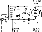 L2 MIXCR S)A ANTENNA L3 22 К Г-мл-, 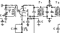 6BJ6 l-F Nl 6BJ6 l-F № 2  4270 С с AVC 9 -IT -euB ТУ OSCILLATOR METER CIRCUIT T -575- 2/~\ l4 (7/uc.) 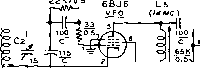 0A2 120 к I* 6AQ5 L6 DOUBLER (гаме. 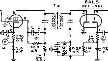 250K 250к 0~ оГь -tW- > im 5-200 = - fo.s о 500 о - L- < о RFC 6.2 к S2  001С L7 Тсз Iclzo pc j35 J ISO . Rl VOLUME MIKE J2 001С 1 Kv NOTES: 1 - CAPACiTOKs marked С .07 ceramic disc, soo v. - - Z-ACC RESISrORS T WATT UNLESS OTHERWISE ЫОГЕО. 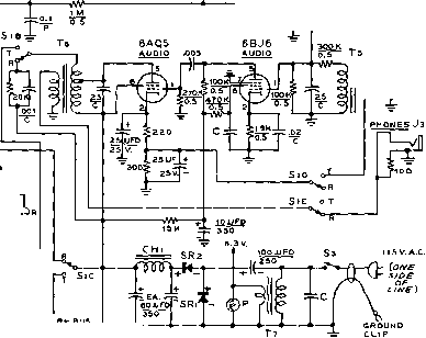 Figure 38A SCHEMATIC, 10 METER TRANSCEIVER с-.07 iiid., 600 vo/t ceramic capacitor. Centralab DD6-I03 RFC-2Уз mh. Millen miniaturized J300-2500 CiA-B-C-?5 /ijuW. per section. All Star Products Co., Defiance, Ohio, Type C3 SiA-B-C-D-E-F-б pole, two position switch. Centralab PA-2019 C,-15 /ififd. Bud MC-565 SR SRt-150 mo. selenium rectifier. Federal 1005 Cj-30 iifd. Bud LC-1651 Ti-Tt-7500 kc. I-f transformer. J. W. Miller Co. 12-W1 Ci-400 iififd. Allied Radio Co., Chicago, III. #6lH-009 Ts-lOO ohms pri. to grid. Triad A-5X Cs-7 /L/Lfd. Erie 532B T,-S К pri., 6.7 К and 4 ohm see. Triad M-4Z CHi-3 henry at 100 mo. Stancor C-2304 Tr-6.3 volt, 3 amp. Stancor P-6466 Chassis and cabinet--California Chassis Ca. #LTC-470 FIGURE 38B COiL TABLE, 10 METER TRANSCEIVER Ll - ANTENNA! 2. TURNS N IB INSULATED WIRE AROUND COLD END OF Ll. CRIDi 14TURNS N ieE., 1/4 DIAM., l/ZLONS. J.W.MILLER 144T-F L2- 13 TURNS Ы* le E., SAME AS Ll Ls-7 TURNS N IB E., SAME AS Ll, TAP AT 3 TURNS FROM SROUND END. l4- 13TURNS № le E., 3/4 DIAMETER, 1/2 LONG. NATIONAL ЛЯ-вг FORM. Ls- J.W. MILLER FORM 14AT-F, 1/4 DIAM., 1/2 LONE CLOSEWOUND WITH N* Zb E. FULL LENGTH OF SPACE. Le- 14 TURNS N le E., SAME AS Ll l7- 7 TURNS N 18 E., 5/8 DIAM., 3/aLONC {BtWSTOCKS
is inserted in a wall socket incorrectly nothing will happen. The transceiver simply refuses to function, and no dangerous situation is created. Simply reversing the plug will energize the circuit, with no danger to the operator. The dual power lead connection, therefore, is a simple and foolproof system of protection and permits the use of the inexpensive and light weight selenium supply. The only other practical alternative is to employ a power transformer which will add excessive weight and bulk to the package. Because this hazard exists with any radio equipment of the so-called ac-dc type, many of the newer buildings are being wired with polarized power receptacles having a separate grounding pin. The use of this new wiring technique will help to reduce the inherent shock potential of the practical and efficient half-wave rectifier systems, of which this is an example. Transceiver Layout and Assembly The component placement may be seen in figures 39 and 40. The 28-10 transceiver is built upon an aluminum chassis measuring 11 x 8У2 x 2 in size, and fits within a steel wrap-around type cabinet 5?4 high. The cabinet is formed of perforated metal to ensure proper ventilation. Radiation of harmonics from the assembly is reduced to a minimum with this type of enclosure. Layout of the major components above the chassis may be seen in figure 39- The receiver Figure 39 REAR VIEW OF TRANSCEIVER CHASSIS Tuning capacitor of variable frequency oscillator is in foreground of photo, panel driven by an extension sftaft. To the left of the copaertor is the adiustable slug core of the oscillator coll. Along rear edge of the chassis are the selenium rectifiers, the filament transformer and the high voltage filter capacitor. Transmitter tubes are at right of chassis, with am-pPifier tube next to рапЫ. At tar right is voltage regulator tube. Audio section is at upper left with 9006 diode rectifier in front ot the input audio transformer. I-f amplifier is at center chassis, parallel to front panel. 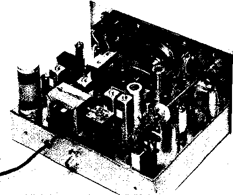 section of tlie unit occupies the center section of the chassis with the power supply directly behind it. To the right is the transmitter section with the variable frequency oscillator at the rear. Panel control of the oscillator is accomplished by an extension shaft and a flexible coupling. At the left of the chassis is the audio system. Placement of the main tuning dial is dictated by the height of the three-gang tuning capacitor shaft above the chassis deck. In this case, it is necessary to cut a small notch in the soft aluminum chassis to permit the dial drive assembly to drop low enough to permit the dial shaft to align with the capacitor tuning shaft. No interstage shields are required below the chassis. Filter choke CHI mounts at the rear of the chassis, directly below filament transformer T?. The 100 fififd. filter capacitor mounts to the left wall of the chassis below and to the left of v-f-o tuning capacitor Сг. The three slug-tuned coils of the receiver may be seen in the photograph. Coil Li is located behind change-over switch Si. Coil Ls is towards the middle of the chassis, and adjacent to the 10 fiid. audio decoupling capacitor. Coil La is to the left of L2 and between the r-f tube and mixer tube sockets. The transmitter oscillator coil h is placed at the left rear corner of the chassis. The adjustable slug of this coil is visible in figure 39 between the selenium rectifiers and tuning capacitor C2. To facilitate wiring, four phenolic tie-point terminal strips (six lug type) are placed beneath the chassis. One is located parallel to the edge, just to the left of the 6AQ5 buffer tube socket. A second is placed parallel to the first, to the right of the same socket. The latter strip is used for connections to the r-f circuitry of the receiver section. The third strip is placed parallel to the rear of the chassis just in front of the i-f strip and is used for i-f connections. The last strip is located between the 6AL5 tube socket and the main fiher capacitor. The noise limiter and a-v-c components are mounted to this strip. To secure maximum srability it is necessary to firmly mount the oscillator tuning capacity to the chassis. An aluminum block measuring lYs X 1 was therefore cut from a section of Vl-inch aluminum stock and used as a support block for capacitor C2. The capacitor is bolted to the chassis by long 6-32 machine screws which pass through the block and are firmly bolted beneath the chassis. 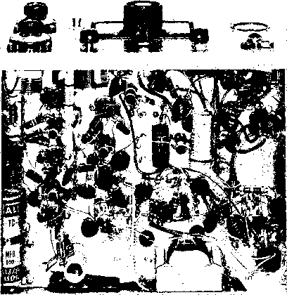 Figure 40 UNDER-CHASSIS VIEW OF TEN METER TRANSCEIVER The transmitier cam-ponenii are alortg the left side of the chassis. Receiver componertts are at the center, with r-f stage nearest the panel. Filter ehoJke f* mounted below chassis at rear. Audio stage components are grouped in upper right corner of chassis. See text for placement of the smaller components. 3-WIRE HOUSEHOLD WIRING Cl RCUIT HOT LEAD OF TRANSCEIVER POWER SUPPLY GROUND LEAD OF TRANSCEIVER POWER SUPPLY Figure 41 GROUNDED NEUTRAL WIRING SYSTEM Most dwellings have a three-wire grounded neutral system. 715 vo/ts a-c can be obtained from either side of the system to ground. Separate ground lead on transceiver is always connected before line plug Is energted. This eliminates usual ac-dc shock hazard. Transceiver The sequence of wiring follows Wiring much the same pattern as that of the six meter transceiver described in section 27-6. Small components are installed between tube socket pins, or between socket pins and adjacent terminal strip lugs. Socket ground connections are made first and then the filament wiring is completed. The power supply wiring can be done first. When the supply is completed it should be tested. A 2500 ohm, 25-watt resistor should be attached between the output of the supply and ground. A full 250 volts should be developed across this resistor with 115 volts a-c applied to the power supply. Next, the i-f and second detector section of the receiver should be wired. Short, direct leads and the use of the adjacent terminal strips will reduce crowding in this area. The audio stages should now be wired, along with switch segments SIB, SID, and SIE. When this is completed, the i-f section and audio of the transceiver may be tested. A test speaker should be connected to jack Js, and a 1.5 Mc tone modulated signal from a test oscillator is loosely coupled to the plate pin (#6) of the 6U8 socket. The top and bottom slugs of the i-f transformers are now adjusted for maximum output signal. As the stages approach alignment, be sure to decouple the signal generator to prevent overloading. After this portion of the transceiver has been tested, the r-f circuits of the receiver should be wired. Coils Li, La, and La are wound and the coil forms clipped in place. The front section of tuning capacitor CIA is employed for the grid circuit of the r-f stage, the middle section is for the interstage r-f circuit, and the rear section is for the oscillator section of the 6U8 tube. Connections between the coils, the tuning capacitor, and the tube sockets are made with #16 tinned solid wire. In particular, care should be taken to prevent movement of the leads and components in the oscillator section as any minute vibration of this part of the circuit would lead to receiver instability. Sufficient coupling exists between the wiring of the oscillator and mixer circuits to provide the proper level of injection, and no coupling capacitor is required. The final wiring step is to wind the antenna coil on form Ll. One end is attached to a nearby socket ground lug and the other end goes to the receive contact of transfer switch SIA. When the receiver is completed, a 28.5 Mc may be injected into the antenna circuit and the main tuning dial set near maximum capacity. The slug of receiver oscillator coil Ls is now adjusted until the signal is received near a dial setting of thirty degrees. After this, coil Ll and coil Ls are peaked for maximum signal strength. Dial caUbration should wait until the transmitter section is completed. Completion of the The oscillator coil should Transmitter Section be wound and mounted in position. The lead from coil L4 to tuning capacitor C2 is made of #14 solid copper and passes through a M-inch hole in the chassis- All oscillator components are firmly mounted to reduce vibration to a minimum. Coils Ls and Ь are wound and snapped into position as the buffer stage is being wired. The p-a plate coil (Lj) is mounted above chassis between the 6AQ5 amplifier tube and the front panel. The plate (or hot ) end of the coil is supported on a Vi-inch ceramic insulator and the coil lead passes through a 14-inch hole in the chassis to the stator of tuning capacitor Сз, mounted directly below the coil. The opposite end of coil L? is attached to a polystyrene feed-through insulator. Neutralizing capacitor Ce is affixed at one end to a terminal of coil form Le. The other end attaches to the plate r-f choke, as shown in the under-chassis photograph. The output lead from transfer switch SlA to the antenna receptacle on the rear of the chassis Is made from a short length of coaxial cable. When the wiring is completed all connections should be checked and the chassis thoroughly cleaned of solder bits, pieces of wire, flux, etc. Transmitter The 6BJ6 oscillator tube should Adjustment be placed in the socket, along with the 0A2 voltage regulator. Transmitter frequency control capacitor Cs is set near full setting and the slug of oscillator coil Li is adjusted so as to place the oscillator frequency on 7.1 Mc. The fourth harmonic of the oscillator will then be on 28.4 Mc. At minimum tuning capacitor setting the upper frequency limit of the transmitter will be slightly above 29-7 Mc. The 6AQ5 tubes are now placed in their sockets, and a 0.5 d-c milliammeter is temporarily connected across meter shunt Ri in the grid circuit of the 6AQ5 final amplifier stage. The screen lead (pin 6) of the 6AQ5 amplifier tube is temporarily opened. Transfer switch Si is placed in the transmit position and the v-f-o tuning capacitor Сг is set to 29 Mc. The transmitter is energized and the slugs of oscillator coil Ls and buffer coil Lc are adjusted for maximum grid drive to the amplifier (about two milliamperes). Amplifier loading capacitor d is set at full capacity, and tuning capacitor Сз is tuned through its range while carefully noting the grid current reading. The reading will show an abrupt kick as G is tuned through resonance. Next, the setting of neutralizing capacitor Cs should be slowly varied by means of a fibre-blade screwdriver so as to minimize the kick of grid current. After each movement of Cs, the slug of coil Le should be reset for maximum grid current. A setting of G can readily be found that will provide a minimum value of grid current change as capacitor Сз is tuned through resonance. The last step is to resolder the screen lead to pin 6 of the 6AQ5 amplifier tube socket. Transceiver The transmitter may now be Operation attached to a suitable antenna or dummy load (see section 27-6) for an operative check-out. Receiver calibration should be rechecked, and the dial may be calibrated. The transfer switch should be set to the transmitting position and the transceiver loaded into the antenna system. The meter now indicates the r-f voltage rectified by the 9006 diode attached to the output of the pi-network system. Tuning (Сз) and loading (C4) should be adjusted to provide a maximum meter reading, with Сз always being set last for the final touch up adjustment. Maximum capacity setting of G provides minimum loading and vice-versa. It may be necessary when working into low impedance loads, or transmission lines having a high value of SWR to parallel loading capacitor G with an auxiliary 100 ayxfd. mica capacitor to obtain optimum loading. This will have to be determined by experiment. A mobile carbon microphone may now be plugged into jack Ja. An indication of the modulation level can be obtained by noting the increase in brilliance of the lamps of the dummy antenna. Overloading will tend to cause downward modulation. The degree of modulation may be varied by moving the microphone away from the lips. Using a telephone-type V-1 unit, optimum modulation occurs when speaking in a normal tone about three inches from the microphone- The transceiver output is about six watts fully modulated with a power amplifier input of ten watts.  The exciter is the heart of the amateur transmitter. Various forms of amplifiers and power supplies may be used in conjunction with basic exciters to form transmitters which will suit almost any need. Of great interest today are simple SSB exciters for fixed and mobile operation. These may be used as-is or with a small linear amplifier for mobile work, or may be combined with a high power linear amplifier for fixed station operation. Also occupying a position of importance is the package VHF station capable of operation on one or more of the VHF amateur bands. Several different types of equipment designed to meet a wide range of needs are described in this chapter. There are two different sidband exciters for fixed/mobile service and a de-luxe VHF station capable of outstanding performance on two VHF amateur bands. Also shown is a high stability variable frequency oscillator unit designed for operation in the high frequency DX bands. To the amateur who is interested in the construction phase of his hobby, these and other units shown in later chapters should offer interesting ideas which might well fit in with the design of his basic transmitting equipment. As in the previous chapter, the component nomenclature and color codes outlined in figures 1, 2, and 3 of chapter 27 are used in this chapter unless otherwise noted. 28-1 SSB Exciter for Fixed or Mobile Use The simplest and most economical method of generating a single sideband signal is to employ a phasing-type transmitter of the form outlined in chapter 17 of this Handbook, If the r-f phasing system operates on the carrier frequency of the transmitter the complex frequency conversion circuits may be omitted and the complete exciter becomes inexpensive to build and simple to place in operation. A SSB exciter suitable for fixed or mobile operation is shown in figures 1 and 4. The exciter delivers a 3 watt peak power signal, sufficient to drive a high povier tetrode linear amplifier to a kilowatt level. Operation is confined to the 80 meter band, although operation on the higher frequency bands is possible with a change of coils, phasing network, and crystal. The r-f phasing circuits are balanced at some frequency within the amateur phone band and will, retain a good degree of balance over a frequency range of plus or minus fifty kilocycles of the adjustment frequency. Circuit The circuit of the single side- DescripHon band exciter is shown in figures 2 and 3. A 12AU7 is employed as a crystal oscillator stage and buffer-amplifier. The first section of the double triode is used in a Pierce oscillator circuit with the crystal connected between the grid and plate of the tube. The oscillator operates directly on the chosen SSB frequency in the 80 meter band. The frequency of oscillation may be varied over a range of two hundred cycles or so by the 50 fi/iid trimming capacitor permitting the transmitter to be zeroed in on a particular SSB channel. The second section of the 12AU7 serves as an isolation amplifier with the plate circuit tuned to the operating frequency. Changes in the input impedance of the diode modulator stage under operating conditions would cause frequency shift of the oscillator stage if direct coupling between these circuits was used. The isolation afforded by the buffer stage effectively prevents frequency pulling of the oscillator stage during modulation. The output of the buffer stage is link coupled to a simple 90° r-f phase shift network wherein the audio signal from the audio phasing amplifier is combined with the r-f signals. The network is of the R-C type made up of 50 ohm non-inductive resistors and 800 fifiid. capacitors in a bridge configuration. The reactance of the capacitors is very close to 50 eOM. 12AU7 A-1N81 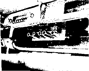 DIODE MODULATOR 6CL6 aw.ssB SIGNAL 12AU7 XTAL
CAIN У CONTROL Figure 2 BLOCK DIAGRAM OF PHASING-TYPE SIDEBAND EXCITER Only five tubes are required in this simple phosing-type sideband exciter. Audio system has sufficient gain to operate from crystal microphone. ohms in the center of the 80 meter phone band. Bridge balance and carrier eUmination is achieved by adjustment of the variable potentiometers (Re, Ra, Rio) in the bridge circuit. Four selenium diodes are used in the modulator circuit. A 1N82 multiple diode assembly may be employed, or four 1N81 diodes whose front/back ratios are equal may be used. The output of the balanced modulator network is coupled by a low impedance link to the grid circuit of a neutralized 6CL6 linear amplifier. This stage operates class ABi with cathode bias, delivering a 3 watt peak SSB signal to a low impedance load circuit. All circuits are tuned by adjustable slug-tuned coils (Ll, Ъ, and La). A cascade 12AU7 and a 6C4 comprise the speech amplifier which may be driven from a crystal microphone. The output of the 6C4 is transformer coupled into the audio phase shift network PS-1. An interstage transformer is connected backwards for Ti, providing a relatively low impedance secondary winding delivering two equal audio voltages that are 180° out of phase. These voltages are applied to the special audio network whose output circuits drive separate triode sections of the 12AU7 audio phasing amplifier. The 12AU7 tube functions as a dual cathode fol- Figure T THE GLOVE COMPARTMENT SIDEBAND EXCITER This miniature phasing-type SSB exciter may be mounted in the glove compartment of a car with room io spare! Using only four tubes the exciter delivers a 3 watt peafc sideband signal capable of driving a kilowatt tetrode amplifier to full output. The J2AU7 and 6CL6 r-f tubes are at the right end of the chassis, along with the crystal. Major tuning controls are on the right end of the chassis. Entire unit is bolted to the roof of the glove compartment. lower which provides the necessary low impedance required to match the r-f phasing network. Sideband switching is accomplished by reversal of polarity of the audio channels by switch Sl. The diode modulator may be unbalanced to pass a carrier for tune-up purposes by throwing carrier insertion switch Ss to the right pjid biasing the diode modulators by means of carrier insertion control R?. Power requirements for the transmitter are 300 volts at a current drain of 100 milliamperes, and 6.3 volts d-c at 1-85 amperes. When the filaments are connected for 12.6 volt op- 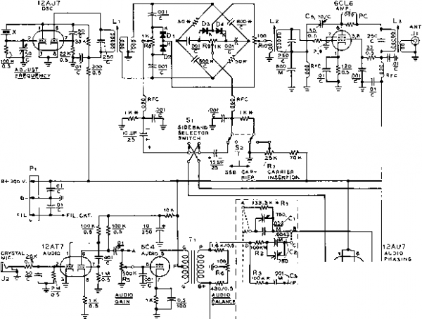 FILAMENT CONNECTIONS -----TJUJoj 7C4 S 300
12AU7 OSC. 6CL6 AMP 12AU7 AUDIO eC4 AUDIO 12AU7 AUDIO 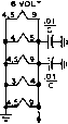 12 VOLT 4A5 10 n. 5W. с LE iia.4l5>tR4. J PS-1 (S££ FIGURE 7 ) NOTE Sl с - MA TCHED COMPONENTS ( I It, 0Я LESS). EXACT VALUE CRITICAL ONLY IN THAT IT SHOULD MATCH THE MATING UNIT CLOSEL У. TO Pi Figure 3 SCHEMATIC DIAGRAM OF FIXED/MOBILE SSB EXCITER Cl, Cl, Сз, Ci-See figure 7 Cs-10 lififd variable ceramic, Centralab 827B. Rl, Rt, Rs, Ri-See figure 7 Ri-500K linear taper potentiometer Rs, Rm-IOO ohm potentiometer Rr-25K linear taper potentiometer Rs, Rs-IK potentiometer PS-1-Phase shift networlt pacltage. See figure 7 Ll, Ll, Ls-See figure 8 Ti-Interstage audio transformer (1:3). Stancor A-53C used bacliwards. RFC-Miniature 2.5 mh. choke. MUfen mO-lSQQ X-80 meter crystal (3800 - 4000 kc.) PC-3 turns #18 e. wire around SO ohm, 0.5 watt composition resistor. Di-Di-IN8I diodes; see text.  Figure 4 TOP VIEW OF SSB EXCITER The top plate is removable for easy access to internal wiring ond adjustments. Microphone jack ond coaxial antenna receptacle are visible at left of chossis. four control potentiometers are along bottom of box (see text). eration current the current drain is 1-25 amperes. TransmiHer The transmitter is constructed Construction upon an aluminum box-chas-and Wiring sis measuring 10 x lYi x 2Y2 in size. Placement of the major components may be seen in figure 5. The 80 meter crystal and 12AU7 oscillator/buffer tube are positioned at the left end of the chassis, and the 6CL6 linear amplifier is centered on the chassis. The balanced modulator is mounted on a phenolic terminal board on the opposite side of the box. Oscillator tuning controls are placed on the left side of the box-chassis, along with the sideband selector switch Si, the carrier insertion switch S2, and the audio gain control Re. Along the bottom of the chassis are placed (left to right) the modulator balance potentiometers Rs, Rn, and Rio and the audio balance control Re. The carrier insertion potentiometer R? is mounted inside the chassis. The three audio stages are mounted on the right-hand section of the chassis. The components of the audio phasing network PS-1 are mounted on a small phenolic terminal board that may be observed in the lower right corner of the chassis. This network should be wired and tested before it is placed in the transmitter. The Audio Phasing Network The complete network may be purchased as a finished item (Millen 73012} or it may easily be home built if an audio oscillator and oscilloscope are available for testing purposes. The circuit of the audio network is shown   Figure 5 UNDER-CHASSIS VIEW OF SSB EXCITER Placement of the main components may be seen in this inside view of the chassis. R-f circuitry is at the left with home-made audio phasing network at center, right. R-f modulator potentiometers and germanium diodes in lower left area of the chassis with audio section at right. The 6CL6 linear amplifier plate coil i$ in the foreground of the center of the chassis. in figure 7A. The mounting base may be thin phenolic or any insulating material. The base holds four precision resistors and four fixed mica capacitors padded with four adjustable mica trimmer capacitors. If desired, a series of fixed capacitors may be measured on a capacity bridge and hand picked units chosen to replace the variable capacitors after final adjustments have been completed. This was done with the network shown in the photographs- The two 100 К series resistors used in the network are Continental Nobeloy 1% tolerance precision resistors. The 133-3 К resistors, however, were made by taking two 150 К precision Continental Nobeloy resistors and paralleling each of them with a one-half watt 1-2 megohm (plus or minus 10% tolerance) resistor. Careful selection of the 1.2 M units permits close adjustment to the desired target value of 133.3 K. A convenient way to mount the 1.2 M resistors is to slip them inside the hollow body of the precision resistors. The dashed connections should be omitted initially, since the alignment procedure described below presumes that these connections will be made at the proper time only. Adjustment of the Audio Network If a manufactured network is employed no adjustments are required. However, the home-made network must be aligned before it is placed in the transmitter 1 ... 53 54 55 56 57 58 59 ... 80 |
|||||||||||||||||||||||||||||||||||||||||||||||||||
|
© 2026 AutoElektrix.ru
Частичное копирование материалов разрешено при условии активной ссылки |