 |
 |
 |
| Главная Журналы Популярное Audi - почему их так назвали? Как появилась марка Bmw? Откуда появился Lexus? Достижения и устремления Mercedes-Benz Первые модели Chevrolet Электромобиль Nissan Leaf |
Главная » Журналы » Simple coaxial reflectometer 1 ... 54 55 56 57 58 59 60 ... 80 chassis. The network resistors should bear the ratio of 133.3 to 100.0, that is, 4 to 3 as closely as can be determined. If in doubt as to the ratio of the resistors you use, double-check their values on an accurate bridge. The adjustment of the phase shift network now consists only of setting the four capacitors to their proper values, An audio oscillator capable of operation from 225 to 2750 cycles per second (with good waveform) is required, plus an oscilloscope. The oscillator should be carefully calibrated by the method described later. Connect the output of the audio oscillator through a stepdown transformer (Ti will serve nicely) to a 1 К potentiometer (use Ri) with the arm grounded- Adjust the arm position so that equal and opposite voltages appear on each half of the potentiometer. A steady audio frequency signal of any convenient frequency may be used with the oscilloscope acting as the voltmeter for this job. Swing the vertical deflection lead of the scope from one end of the potentiometer to the other and adjust the arm to obtain equal voltages- Hook up a temporary double cathode follower using a 12AT7 with 500 ohms from each cathode to ground and connect as shown in figure 7B. (It will be convenient to provide leads M, N, and 1 and 2 with clips at the ends to facilitate checking). Cathode pins 8 and 3 of the 12AT7 should connect to the H and V deflection amplifiers in the oscilloscope, and the oscilloscope ground connection should be made to the common return of the cathode follower amplifier. First connect lead M to terminal A on PS-1 and lead N to terminal A. Connect leads 1 and 2 to terminal M. (Note that the dashed connections are missing at this stage of ad- 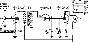 гл /si vox l< ? ON-OF t1 irX/VCO/? Figure 6 SIMPLE VOX CIRCUIT FOR ANY SSB EXCITER Capacitor С and resistor R determine the delay time of the voice operated relay circuit. Operation point is set by potentiometer Ri. Reloy RYi has о high resistance d.c. coil (Automatic Electric Co. type R-4SL with 10,000 ohm coil may be used). justment). Adjust the horizontal and vertical gain controls of the oscilloscope to produce a line about 11/2 inches long slanted at 45 degrees when the oscillator is set to a frequency of 490 c.p.s. (an exact method of setting frequency will be described later). If the oscilloscope has negligible internal phase shift the display will be a straight line instead of a narrow slanting ellipse. If the latter display appears, it is necessary to correct the oscilloscope phase shift externally by using an adjustable series resistance (a 100 К potentiometer) mounted at either the vertical or horizontal input terminal, depending on what correction is necessary. The objective here is to obtain a single straight line pattern on the scope at an audio frequency of 490 c.p.s. In some cases a series capacitor may be needed in conjunction with the potentiometer to provide the necessary correction. Try values from -05 jj-id to -0005 р.И. When the required slanted line is obtained, phase Shift network Ps-1 A 133.ЭК (>-Ш- --oH(- o- -1(-oc eaeoiJjuF IOOK 12I5JJJUF -M--II-OF 607. 5 JUJUF Tl, 1.3 STANCOR AS3-C
AUDIO OSCILLATOR ALL COMPONENTS ± ;5b TOLERANCE  PHASE SHIFT NETWORK PS-1 12AT7 -11 TO VERTICAL DEFLECTION PLATE ►TO HORIZONTAL DEFLECTION PLATE 300 V. Figure 7 AUDIO PHASE-SHIFT NETWORK AND TEST LAYOUT 4rURNS HOOKUP WIRE NATIONAL XP-iO COIL FORM 0/2 DIAM)  BIFILAR CONNECTIONS GROUND LUC NOTE : TWO PARALLEL PIECES OF HOOKUP WIRE ARE WOUND SIMULTANEQUSLr OVER РРШАРУ WINOINS TO MAKE alFlLAP SECONDARY. BOTTOM END of ONE WINOINS AND TOP END OF OPPOSITE WINDING ARE SROUNDED TO MOUNTING LUS ON COIL FORM. Figure 8 BIFILAR COIL FOR SSB TRANSMITTER (Li) CoiVs li and L, have 4-turn link coils over bottom end instead of the bitilar winding. shift lead 1 from terminal A to terminal В on the phase network PS-1. Adjust the trimmer capacitor Ci (figure 3) to obtain a circle on the oscilloscope. It will be noted as this adjustment is made the display will shift from an ellipse leaning to one side through a circle or ellipse (with axes parallel to the deflection axes) to an ellipse which leans the other way. If desired, the appropriate gain control on the oscilloscope may be varied so that a circle instead of an erect ellipse is obtained at the point of correct adjustment. After checking the gain control on the scope, recheck and correct (if necessary) the phase shift in the oscilloscope by moving lead 1 back to terminal A, and then repeat the setting of capacitor Ci with lead 1 back on terminal B. In general, always make certain that the oscilloscope is used in a phase-corrected manner. As a double check (if the deflection plates in the oscilloscope are skewed, for instance) connect lead 2 to terminal A. If the circle changes to a slanting ellipse, readjust G to produce an ellipse half-way between the ellipse (obtained by switching lead 2) and a circle. Changing lead 2 from A to A and back again should give equal and opposite skew to the display when capacitor G is set correctly. Failure to get symmetrical ellipses (egg-shaped, or other display) is due to distortion in the scope, the oscillator, the transformer, or the cathode follower. Conduct the test at the lowest signal level possible to avoid distortion. Next, connect leads M and N to terminals E and E, respectively. Connect leads 1 and 2 to E, set the oscillator frequency to I960 c.p.s., correct oscilloscope phase shift as before, and move lead 1 to terminal G. Adjust capacitor Ci in PS-1 for a circle as was done for G, using the precautions outlined for that case. Now connect lead M to terminal D, and lead N to terminal F. Connect leads 1 and 2 to terminal D, set the oscillator frequency at 1307 c.p.s., correct oscilloscope phase shift as before, and move lead 1 to the junction of Ra and Ca. Adjust capacitor Ca for a circle on the oscilloscope, as before. Repeat the above procedure for the remaining R-C pair, R2 and Ca. Use terminals D and С at this time and set the oscillator to 326.7 c.p.s. This completes the tests except for a final check to all adjustments. Connect A to A, E to E, В to C, F to G, and A to E. The network PS-1 is now completely wired. Checking the Audio Network If the oscilloscope did not require changes in external compensation over the four frequencies used, an over-all frequency check may now be easily made on the phase shift network. To do this, connect lead 1 to point B-C, lead 2 to point F-G, lead M to point A-A-E-E, and lead N to point D. Now shift the arm of the potentiometer towards M until a circle appears on the oscilloscope screen at a frequency of 250 c.p.s. Then, as the oscillator frequency is varied from 250 c.p.s. to 2500 c.p.s., this circle will wobble a little from one side to the other, passing through a perfect circular display at 440, 1225, and 2500 c.p.s. The audio band over which the wobble indicates a plus or minus 1.3 degree deviation from true 90 degrees is 225 to 2750 c.p.s., or 12 to 1 in range. This means that when other circuits are properly adjusted, a sideband suppression ratio of 39 decibels is possible at the worst points within this range. The average suppression ratio will be about 45 decibels. Proper phase-shift network operation is necessary to obtain this class of performance, so the adjustment procedures have been outlined in detail as an aid toward this goal. The phase shift network should never require readjustment, so that when you are satisfied with the adjustment you may seal the trimmers with cement. Audio Oscillator Calibration It will be noted that the frequency ratios are such that the 12th harmonic of 326.7 c.p.s., the 8th harmonic of 490 c.p.s. and the 3rd harmonic of 1306-7 c.p.s. are all the same as the 2nd harmonic of I960 c.p.s.., namely 3920 cp.s. Thus, if a stable source of 3920 c.p.s. frequency (such as a thoroughly warmed audio oscillator) is used as a reference, the frequency of the test oscillator can be set very closely to one-half, one-third, etc- of the reference frequency if both oscillators feed an oscilloscope and the resulting Lissajous figures observed, as discussed in chapter 9 of this Handbook. Use of a calibrating frequency in this manner assures that the frequency ratios used are correct, even though the exact frequencies used are unknown. The frequency ratios (just as the resistance ratio previously mentioned) are far more important that the actual values of frequency (or resistance) used. Transmitter The r-f and audio sections of Wiring the unit should be wired before the phase network is placed within the chassis. Socket ground connections and filament wiring are done first. The oscillator section should be wired and tested first. The bifilar secondary winding of coil Li may be made of two lengths of insulated hookup wire wound over the coil as shown in figure 8. The germanium diodes in the modulator section deserve special care in handling. Do not bend the leads close to the diode unit itself. The diodes are mounted by means of their leads between the terminals of potentiometers Rs and r9 and adjacent tie-point terminals. Protect the diodes from excessive heat while soldering by holding the lead with pliers between the body of the diode and the point where the soldering takes place. Further, use only as much heat as is necessary to make a good joint. The 50 ohm composition resistors used in the modulator bridge circuit should be a matched pair, measured on an ohmmeter or Wheatstone bridge- In the same fashion the bridge capacitors should be matched as closely as possible to the target value of 800 /x/fd. Both coils Ls and Ls of the linear ampHfier are mounted beneath the chassis on either side of the 6CL6 tube socket. To reduce coupling between the coils, a shield is placed over coil L=. The shield may be made from part of an old i-f transformer can measuring approximately 1 X 1 X 2 in size. When the transmitter wiring is completed, the audio phase network PS-1 may be placed in the transmitter chassis and wired in place. Transmitter After the wiring has been com-Adjustment pleted and checked the transmitter is ready for adjustment. Insert the 12AU7 oscillator/buffer tube in the socket, and plug in a crystal in the range of 3.8-4-0 Mc. Apply plate power and adjust the slug of coil Lt for maximum signal strength of the oscillator in a nearby receiver. The oscillator should start promptly each time plate voltage is applied to the unit. Frequency of oscillation may be varied over a small range by changing the setting of the crystal tuning capacitor. The next step is to neutralize the 6CL6 linear amplifier. It is necessary to bypass the diode modulator to do this. Temporarily disconnect one lead of the bifilar link winding on Ll, and also disconnect the lead between potentiometer Rio and amplifier grid coil Lj. Now, connect the free winding of the bifilar link of Ll to the ungrounded end of the link of L2. This will apply the oscillator signal directly to the linear amplifier. Temporarily load the 6CL6 stage with one or two flashlight bulbs (6.3 volt, 150 ma- - brown bead) connected in parallel at the output jack Ji. The slugs of coils L-i and La should be adjusted for maximum amplifier output. The 12AU7 oscillator tube should now be removed from the socket, and unless the setting of neutralizing capacitor G happens by chance to be correct, the flash lamp load will continue to give some indication of output, showing that the 6CL6 amplifier stage is oscillating. Neutralizing capacitor Cs should be adjusted with the aid of a fibre screwdriver until the bulb goes out. Readjust Ъ. and La for maximum bulb indication as the setting of capacitor Сг is varied. A setting of Cs will be found at which oscillation will not occur, regardless of the setting of the slugs of coils L2 and Ls. When Cs is properly adjusted, the 12AU7 tube should be replaced in its socket and coils L2 and Ls returned for maximum output. The temporary link connection between Li and Ls should be removed and the diode modulator reconnected into the circuit. Next, remove the r-f tubes and insert the three audio tubes in their respective sockets. Apply a low level audio signal of 1225 cp.s. to the microphone jack Ji- of the unit and connect the horizontal deflection terminal of the oscilloscope to a cathode (pin 3) of the 12AU7 audio phasing amplifier, and the vertical deflection terminal to the other cathode (pin 8) after making certain that the scope is phase-compensated at the test frequency of 1225 c.p.s. Adjust audio balance control Rc to produce a circle on the screen. Make this test at as low an audio level as possible. Now, plug in the r-f tubes and connect the dummy load to the antenna receptacle, Ji. Connect the vertical plates of the oscilloscope (no scope amplifier used) to the terminals of the dummy load so that the 80 meter signal of the transmitter may be seen on the screen of the scope. Deliberately unbalance one of the diode modulators by setting potentiometer Ro off-center. Adjust amplifier output coil for maximum pattern deflection at any convenient sweep speed. As the pattern grows when La is resonated it may be necessary to reduce modulator unbalance to keep from overloading the output stage or the scope. Remove all audio input to the transmitter by adjusting audio gain control Rs to zero, then by successive adjustments of the modulator balance controls adjust for zero output as seen on the oscilloscope. It will be noted that as the correct point is approached the adjustments will become pre-gressively sharper. Potentiometers Rs and Rs should be juggled until the indicated carrier is a minimum. Slight capacity unbalances within the modulator bridge may prevent a perfect minimum from being obtained. It may be necessary to place a small 10 /xfd variable ceramic capacitor from either end of potentiometer Rio back to one side of the diode rectifier bank for best attenuation. Good carrier attenuation may finally be achieved by juggling the settings of Rs, Ra, and Rw, together with the added padding capacitor. Nexr, apply a 1225 cp.s. audio signal and advance gain control Rs. An r-f envelope should be seen on the screen of rhe oscilloscope. The percentage of modulation (or ripple) noted on the pattern is an indication of the degree of mis-adjustment of the balancing controls of the unit. The balance potentiometers should now be touched up to produce minimum modulation on the observed carrier. Audio balance control Rb should also be checked for minimum ripple pattern. It is a good idea to vary the audio level input to the transmitter to determine the point of overload. This can be seen on he scope as the point at which the modulation ripple on the pattern increases sharply as Rs is advanced. Always make sure that your audio level is set well below this overload point when adjustments are being made. It should be possible to produce a pattern having very little ripple on the observed carrier wave. This completes the adjustments of the transmitter. Carrier insertion for test purposes may be obtained by reversing switch S: and adjusting carrier insertion control R;. transmitter are desirable for serious sideband work, and are doubly suited for mobile operation, since full attention may be given to road problems. A simple voice control (VOX) circuit suitable for use with this transmitter is shown in figure 6. Connection to the speech amplifier is made at point A of figure 3- The voice signal is amplified by a triode stage and rectified by the 6AL5 diode. The resulting signal is applied to the second half of the triode tube which operates a sensitive relay connected in the plate circuit. The relay contacts operate the changeover circuits of the transmitter. The time delay required to make the transmitter hang on between syllables of speech is determined by the R-C network in the grid of the relay control tube. Increasing the size of the capacitor will increase the delay time and vice-versa. 28-2 A Mobile Transistorized SSB Excifer Power consumption of radio equipment is of paramount importance in mobile systems-Without the addition of auxiliary expensive  VOX Circuits Voice control of the send-receive circuirs of the Figure 9 TEN THOUSAND MILES OF QSOS HAVE BEEN MADE WITH THIS TRANSISTORIZED FORTY METER SSB EXCITER r/ie reliability of transistorized sideband equipment has been proven with this miniature phasing-type exciter. Overall size is only 7Ул X * X 2У2 . Antenna, power, and microphone connectors are on end of chassis and balancing potentiometers and buffer base inductor (Li) are mounted on side of chassis. charging components, the usual automotive electrical system is capable of a relatively small additional povifer drain over and above the standard equipment provided with the car. Single sideband affords an excellent opportunity for the mobile enthusiast to obtain more talk power for a given degree of primary power consumption. In addition, if the sideband equipment can be transistorized the power drain will be reduced by a further important amount. Described in this section is a 40 meter experimental transistorized sideband exciter delivering sufficient output to excite a tetrode linear amplifier to one kilowatt peak input power. The exciter operates directly from the 12 volt ignition system of the car, using five inexpensive transistors, a printed circuit transistor amplifier, and a single vacuum tube. Until a power transistor is developed for r-f service, it appears that the vacuum tube will still be necessary as a buffer when high frequencies are involved. Power requirements for the exciter are 300 volts at 50 milliamperes, and 12.6 volts at 0.43 amperes. A new subminiature printed circuit amplifier (Centralab TA-11) is used for the speech amplifier. Completely sealed in epoxy resin for protection against mechanical abrasion and humidity, this four stage transistor amplifier provides a gain of over 70 decibels. The complete unit is only 14 inches long and less than one inch high. It is strongly recommended that spare transistors be on hand for substitution in the various circuits. This will give the builder confidence and assurance that each stage is functioning as it should. Many times Hmitations on performance are imposed by certain transistors without the operator being aware of the con- 1EBY7A ci (тт 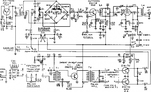 notes: 1, ли COMPONENTS MARKEO * APE f 9b TOLERANCE. EXACT VALUE CRITICAL ONLY IN THAT IT SHOULD MATCH THE MATING UNIT CLOSELY.
Figure 10 SCHEMATIC OF TRANSISTORIZED FORTY METER SSB EXCITER Cj-2Sjj.jj.fd. Variable ceramic capacitor. Centralab 823-DZ L,-35 turns #22 enamel, /3 diam., elosewound on Hational XR-50 form. Start with two turn bifilar winding (see figure 8, section 28-1 for bifilar detail). Mount coil assembly in small shield can. Lz, L.-Some OS L,. Mount 1.. in small shield can. Lj-Same as L,. Tap 18 turns from cold end. Mount in small shield can. RFC-2.5 mh. miniature r-f choke. Millen J300 - 2500 T,- IK pri., 60 ohm see. transistor transformer, Chicago UM-111 Тг-95K sec, ISK pri. [use bdckwords; VrC-07 CH,-200K pri., 1 К sec. transistor transformer. Use primary only. Chicago UM-112 X-7.2 - 7.3 Mc crystal Di-D -Matched 1N81 Diodes; see text. dition. The concept of transistor action is new and novel to many amateurs; it is not easy to run to the corner radio store and test a transistor to make sure it is operating properly. Exciter The complete schematic of the Circuitry transistorized exciter is shown in figure 10. It is derived from the vacuum tube exciter circuit of figure 3, section 1, and employs phasing technique on the frequency of operation. A 2N112 transistor is used as a grounded emitter crystal oscillator employing crystals in the 7.2 - 7.3 Mc. range. The r-f output is coupled through a tuned circuit and a bifilar winding to the crystal diode balanced modulator. The output in turn drives a 2N114 r-f amplifier stage, operating in grounded emitter configuration. A base bias potentiometer Ki is included in this stage which permits parameter adjustment for maximum output. The collector of the transistor is tapped at a point on the grid inductor of the linear amplifier stage providing maximum drive without exceeding the transistor ratings. A 12BY7A is used as the linear amplifier stage. Neutralization is employed for greatest circuit stability, and VHF parasitic oscillations are eliminated by the use of a parasitic suppressor in the plate circuit. The subminiature transistorized audio amplifier used in this exciter has a rising frequency characteristic that is well suited for SSB work. However, the rising response carries well into the upper audio range wherein the phase shift networks of the PS-1 unit cease to function properly. It is therefore nec- essary to incorporate a simple low-pass filter that will substantially eliminate all audio frequencies above 3000 cycles. Such a filter is incorporated in the circuit between the microphone input jack J2 and the transistorized audio amplifier. The filter consists of the primary winding of a small audio transformer (CHi) and two 250 ju.ju.fd capacitors. The output signal from the encapsulated transistorized amplifier is transformer coupled to a 2N250 (or a 2N255) power transistor which serves as a driver for the phase shift network. The 2N250 transistor requires a heat sink for the collector to allow maximum collector dissipation rating to be achieved. The transistor may therefore be mounted on ano-dized aluminum discs or mica wafers (supplied by the manufacturer of the transistor), thus insulating the case of the transistor (the collector terminal) from the chassis of the exciter. The phase shift network driven by this transistor is identical to that described in section 28-1 and illustrated in figure 7- Two 2N170 NPN type transistors are base driven by the phase shift network, and serve as emitter followers, providing a low impedance driving source for the balanced modulator. Sideband selection is accomplished by switch S2 whose purpose is to reverse the phase of the audio signals applied to the balanced modulator. Carrier injection is accomplished by potentiometer Rs and switch Si which apply conducting bias to the modulator diodes. A voltage dropping network is employed 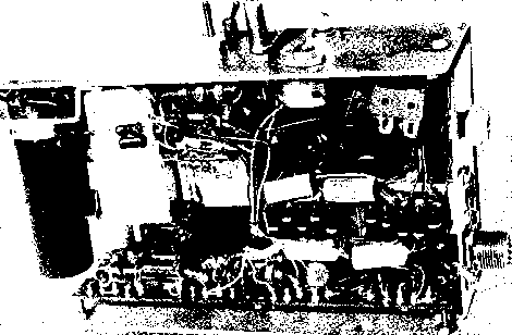 Figure 11 UNDER-CHASSIS VIEW OF TRANSISTORIZED SSB EXCITER The audio and r-f networks are mounted on a phenolic sheet attached ta the bottom of ihe chassis. The I2BY7A linear amplifier and shield are mounted on a small aluminum bracket ai ihe left of the assembly. Grid coil L3 is beside the tube, and plate coil Li is behind the tube. Coil Ll is to the right of Lj with sideband switch St behind it. The two r-f balancing controls Ri and Rt are at the extreme right of the chassis panel. to reduce the 12.6 volt primary supply to 9 volts for the 2N170 stage, and to 4 volts and 2У2 volts for the preamplifier stage. The exciter is designed for use with a primary supply having the positive terminal of the battery grounded. Exciter The exciter is built within Construction an aluminum case measuring 71Д x 4 x IV2 in size. Miniaturization of the audio phase shift network was accomplished by measuring a quantity of resistors and capacitors on a bridge. Final selection was made from those having the closest tolerances. These hand picked components are mounted on a phenolic terminal strip. This same sheet is used to support the small r-f chokes as well as the balanced modulator components. It is a good idea when building equipment to fit in a limited space to construct everything in the form of sub-assemblies. This will permit the components to be mounted in the open, facilitating wiring. In this particular unit, the audio components and the r-f modulator are mounted on a phenolic board on one side of the box and the r-f components are attached to the opposite wall of the box. The oscillator coil Ll is placed within an old i-f transformer can as is the linear amplifier grid coil Ls. The 12BY7A tube is mounted on a small bracket at one end of the box, and has a tube shield placed over it. The plate coil Li of the amplifier stage is directly behind the tube (figure 11). Various voltage dropping resistors are mounted on a small terminal board at the center of the chassis, and the audio transistors are placed in the area between the lower terminal board and the rear wall of the case. The r-f circuits are wired after the component boards are mounted in place. Wiring is straightforward and simple. The two r-f transistors are mounted by their leads to three terminal phenolic tie-point strips. Be sure to protect both the transistors and the modulator diodes from excess soldering heat, as described in section 28-1. The reader is referred to this section concerning the adjustment and test procedure for the home-made phase shift network. Testing The The transistorized SSB exciter Exciter may be bench tested by running the transistors from a group of IV2 volt batteries. It is wise to conduct preliminary tests at an operating potential of about 9 volts. The voltage may be boosted to the operating value after tuning and alignment adjustments have been completed- Volt- age should be first applied to the transistor oscillator. R-f output may be measured at the terminals of the bifilar coil with the aid of a vacuum tube voltmeter. The slug of coil Li is adjusted for maximum reading. Under diode load, about 4 volts r.m.s. may be measured from either side of the winding to ground. The bifilar winding is relatively critical. Too many turns will load the oscillator to a point of instability, and too few turns deliver insufficient drive to the modulator. Two turns, loosely coupled to the primary winding, seem to be about correct. When the bridge is unbalanced, approximately 0.2 volt r.m.s- may be measured from either arm of output potentiometer Rs to ground. This voltage is stepped up by means of a pi-network circuit so that maximum excitation voltage is applied to the base of the 2N114 r-f transistor. Preliminary adjustments, in general, follow those described for the vacuum tube exciter described in section 28-1. Potentiometers Ri, R2, and Rl are adjusted for minimum carrier output in the collector circuit of the 2N114. It may be necessary to add a 10 /A/fd variable ceramic capacitor from one side of the modulator bridge to ground to achieve maximum carrier suppression. The final adjustment is to apply an audio signal and touch up the audio phasing potentiometer Rs for maximum rejection of the unwanted sideband- When these preliminary adjustments have been made, the 12BY7A tube may be inserted in the socket, and the shield slipped over the tube. Grid inductor Ls is resonated for maximum grid excitation with the aid of grid dip oscillator, and the plate inductor Li can be tuned in the same manner. A dummy load consisting of two 6.3 volt, 150 ma. flashlamp bulbs (brown bead) connected in parallel is attached to output jack Ji. Plate voltage and excitation are now applied to the linear amplifier stage and La and L4 adjusted for maximum output. When audio excitation is removed from the exciter the r-f amplifier will probably break into oscillation and the antenna bulbs will continue to glow. Neutralizing capacitor Cl should now be adjusted with a fibre screwdriver until oscillation stops. After the exciter is operating properly, full battery voltage may be applied to the transistor stages with a consequent increase in grid drive and power output of the linear amplifier. Approximately 2 volts r.m.s. grid drive may be measured with the vacuum tube voltmeter at the grid pin of the 12BY7A linear amplifier stage under conditions of maximum excitation. 28-3 A VHF Transceiver of Advanced Design Modern tubes and circuit techniques permit sensitivity and stability levels to be achieved in the VHF region that were possible only at the lower frequencies a few years ago. The transceiver described in this section makes full use of these advanced circuits to produce superb results in the amateur 50 Mc. and 144 Mc. bands. The transceiver (pictured in figure 12) comprises a complete VHF station and power supply in one small, streamlined cabinet. The transmitter section Is crystal controlled on any one of eleven frequencies chosen at random In the two bands, and runs eighteen watts input fully modulated. The receiver section employs cascode-type r-f amplifiers resulting in a noise figure better than 5 decibels on both bands. Optimum communications selectivity is obtained by the use of a two-section crystal lattice filter in the Intermediate frequency amplifier. Maximum frequency stability Is achieved by the use of crystal controlled VHF conversion oscillators and a highly stable low frequency tunable oscillator. A signal strength meter is incorporated in the receiver, and a tuning meter is used to obtain optimum transmitter adjustment. The power supply operates from 115 voits a.c, and eithei 6- or 12-voits d.c. Styling for the transceiver permits Its use either as a fixed, home station or as a mobile unit. The major tuning controls are placed at the left of the panel to permit operation while the automobile Is being driven. A push-to-talk system is employed for rapid break-In operation, and band changing takes place in a few seconds. Twenty tubes including a voltage regulator are employed in the unit, and the total primary power consumption is approximately 105 watts. Circuit This high performance trans- DescripHon ceiver is a complex device, and the wiring diagram has been broken down into several schematic drawings (figures 14, 15, 17, 18, and 19). A block diagram of the complete circuit is given in figure 13. The Receiver Section. The receiver portion of the unit employs thirteen tubes in a double conversion superheterodyne circuit. Separate r-f front ends are employed for each band. Each front end employs a 6BZ7 cascode r-f ampUfier and a 6J6 converter/oscillator tube. The desired section is activated by energizing the filaments and connecting the output circuit of the mixer stage to the first i-f amplifier. Switch S? accomphshes this action. The 144 Mc. cascode amplifier Is neutralized for optimum signal-to-nolse ratio, while the neutralizing circuit is omitted from the 50 Mc. amplifier since a satisfactory noise figure is obtained without the extra coil. Overtone crystals operating in the VHF region are used In a regenerative oscillator circuit to provide mixing voltage for the 6J6 triode converter. The complete schematic of the r-f section is given In figure 14. The tunable intermediate frequency amplifier covers the range of 30 - 34 Mc. Low side oscillator operation is used for two meter operation with the conversion crystal at 114 Mc. High side operation is used for six meter service with the crystal at 84 Mc. The four megacycle i-f tuning range is covered by a 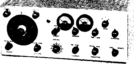 Figure 12 VHF Transceiver for Six and Two Meters is Designed for Fixed or Mobile Operation This transmitter-receiver provides the highest order of reliable communication in the two most popular VHf bands. Receiver tuning controls are placed at the left of the unit to permit ease of tuning in mobile installation. Double conversion receiver and crystal lattice i-f filter provide maximum stability and selectivity for reception. Crystal controlled transmitter delivers a ten watt carrier. Band change iajces only a few seconds. Left hand meter is signal strength indicator for receiver, and meter at right is multi-purpose millammeter for transmitter. The transmitter tuning controls are ai right. Perforated metal cabinet insures maximum ventilation for continuous operation. TV-type rotary induction tuner, padded to the correct operating range. The use of this type of tuned circuit provides exceptional stability combined with small size and has proven to be a very satisfactory choice. A 6Bj6 remote cutoff pentode is used as the first i-f amplifier stage (Vb) and a 6BE6 is used as the second mixer (Ve). The tunable oscillator stage operates 2009 kilocycles lower than the variable intermediate frequency and employs a single section of a 6J6 tube (Y). A small inductance (Lii) is placed in series with the rotary coil of the oscillator section to ensure proper tracking over the 4 Mc. tuning range. The greater portion of the receiver gain and selectivity is achieved in the second intermediate frquency amplifier which operates at a center frequency of 2009 kc. A double lattice crystal filter is employed to ensure maximum selectivity at this frequency. The filter is made in two sections and has a single 6BJ6 amplifier tube (Vs) between the sections to compensate for the insertion loss of the filter. The first section of the filter is placed immediately after the 6BE6 converter tube to achieve maximum i-f amplifier protection from strong signals adjacent to the desired one. Two crystals are used, one at a frequency of 2007 kc and the other at a frequency of 2011 kc, providing a flat top to the passband of about 4 kilocycles. The crystals used in this filter are specially cut for filter work, and the substitution of ordinary transmitter type crystals will degrade the performance of the filter. The units specified in figure 15, however, are not expensive. The i-f transformers are standard 1500 kc. units with the mica tuning capacitors changed as shown in figure 15 to permit operation at 2 Mc. The lattice filter may be removed from the circuit by means of the sharp-broad switch. Si. All four crystals are shorted out in the broad position, and one crystal in each filter section is disconnected from the associated i-f transformer. In addition, another section of the switch (SiC) drops the gain of the amplifier tube (Vs) to compensate for the rise in stage gain that occurs when the crystals are removed from the circuit. Two additional stages of i-f amplification (Vs., Vio) follow the crystal filter, providing an abundance of gain for proper operation of the a-v-c and audio squelch circuits. The detector and associated audio components of the receiver are shown in figure 17. A 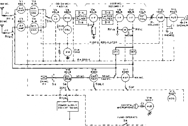 Sio7 POWER V 1 1 5 v. ъ e/12V.d.c, ajdio
Figure 13 BLOCK DIAGRAM OF 2-6 METER TRANSCEIVER Twenty lubes plus selenium rectifier power supply provide de-luxe operation for the advanced VHF enthusiast. Power supply may be operated from either automobile electrical system or 115 volts, a.c. 6AL5 (Vii) is employed as detector, a-v-c, and a-n-1 tube. The noise limiter is of the low distortion type and is left in the circuit at all times. One section of the 6AL5 serves as the a-v-c rectifier, and the resulting voltage is applied to four i-f tubes for smooth a-v-c action on strong signals. The last i-f stage (Vm) is left off the a-v-c line, and the S-meter is connected between the plate supply return of this tube and an adjacent controlled tube. A change in the plate current of the controlled tube (Va) upsets the balance of the bridge circuit, and a meter reading is produced that is proportional to the a-v-c voltage. This voltage is also applied to one section of a double triode audio tube (V12) which functions as a squelch tube. This circuit renders the audio section of the receiver inoperative until the receiver a-v-c circuit is activated, thus eliminating a large portion of the background noise commonly associated with VHF reception. The squelch circuit may be disabled by switch Sa. Two audio stages (V]2 and Угг) deliver sufficient audio power to fully drive a loudspeaker and to overcome the motor and wind noises of a car in motion. An auxiliary jack (]з) provides earphone reception if desired. The receiver is inactivated during transmission periods by relay contacts RY2B which remove the high voltage from the plates and screens of the receiver tubes. The Transmitter Section. Shown in figure 17 is the transmitter section of the transceiver. Six tubes are used, three for the audio portion of the unit and three for the r-f portion. Crystals in the 24 - 25 Mc. region are employed for both 6- and 2-meter operation. Any one of eleven crystals may be selected by switch S2. The oscillator is a 6CL6 (Vu) in a hot-cathode doubler circuit, delivering energy in the 48 - 50 Mc. region. A split-stator tuning capacitor is employed in the plate circuit to provide a balanced output configuration. The oscillator stage may be turned on during re- 144MC, 50 MC Vi 6BZ7A 1ДД MC. SECTION Ls l4 с 470K 1 7.2 к]; ikJc mj ti Ls С с -bte£t. bth.y- 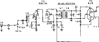 NOTES; 1. see Fis. fe for filament wiring. a. с- .001 disc ceramic 3. ALL resistors гул watt l9 LZ- b± 0* S7A c -oS7D (see fis. le for sections bsc ) - l-F OUT О ® see figure >s Figure 14 SCHEMATIC/ R-F PORTION OF RECEIVER SECTION С-.001 дМ. disc ceramic capacitor. Centralab DD-I02 Cj, Cl-20 /ifitd. Johnson 20M11 J Jl-BNC-type coaxial receptacle L,-Ls-See figure 21 for coil information S7A, D-Pari of 57 (Centralab wafer PA-9} See figure 18. RYiA, RYiA-See figure 19 Xl-114 Mc. overtone crystal. Precision Crystal Lab., Santa Monica, Calif. X,-84 Mc. crystal (see Xj) 1 ... 54 55 56 57 58 59 60 ... 80 |
|||||||||||||||||||||||||||||||||
|
© 2026 AutoElektrix.ru
Частичное копирование материалов разрешено при условии активной ссылки |