 |
 |
 |
| Главная Журналы Популярное Audi - почему их так назвали? Как появилась марка Bmw? Откуда появился Lexus? Достижения и устремления Mercedes-Benz Первые модели Chevrolet Электромобиль Nissan Leaf |
Главная » Журналы » Simple coaxial reflectometer 1 ... 56 57 58 59 60 61 62 ... 80 ATAL V1 AUDIO CATHODE PRODUCT AMP. FOLLOWER MODULATOR V2A V3 l-F AMPLIFIER Vb CAIN CONTROL FIRST 1AMC. SECOND 14 MC. AMPLIFIER AMPLIFIER 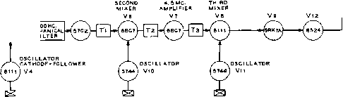 I CRYSTAL Xl 498 KC CRYSTAL x 2 400 2 KC. CRYSTAL ХЭ 9.7-9.В MC. +475 +125 +300 I [ l-AaoA POWER SUPPLY 115/ 230V. 50-60 4, V13 V14 REG. REG. LAYOUT, CHASSIS* 1, SIDE* 1 r-V3 AND SHIELD v4 A SH1EL О; MECHANICAL FILTER e r3 LAYOUT, CHASSIS *1, FRONT
LAYOUT, CHASSIS * 1, SICE*2 Ve AND ELD V7 AND. SHIELD SHIELD fv о SHI О о WVii ,rV9 *ND 4 jmnD lELD *\ Jl KJ ---SHIELD Figure 24 BLOCK DIAGRAM AND PARTS LAYOUT OF 14 MC. SIDEBAND TRANSMITTER Fourteen tubes (including two voltage regulators) are used in this compact transmitter. A Crosby modulator and 500 fee. Collins Mechanicai Filter are employed for sideband generation. First frequency conversion is to 4 Mc, and second frequency conversion is to 14 Mc. Layout of major components on both sides and front of special chassis is shown in the ilfustratjon. Figure 25 OBLIQUE VIEW OF AMPLIFIER AND EXCITER CHASSIS The power amplifier chassis is at the left. The plate coil, plate tuning capacitor and loading switch are In the foreground. Side #1 of the exciter is shown. The Inter-chassis area is covered with perforated metai. The tip faclts for the receiver disabling circuit are on the right edge of the chassis. Corners of the mounting base are rounded to permit close tit with rounded corners of drawn aluminum case. 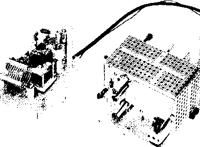 ployed with the linear amplifier stage. In order to conserve space, the usual variable capacitor is omitted from the output side of the network and a rotary switch and selection of fixed capacitors is employed in its place. Proper choice of capacitors permits the transmitter to be matched to 52- or 72-ohm transmission lines having s.w.r. values as great as 2.5/1. The problem of obtaining the necessary d-c power from a supply that would fit within the small cabinet space was solved by employing a bridge rectifier using the new Sarkes- Tarzian silicon rectifiers. The forward voltage drop of these rectifiers is of the order of only 1.5 volts and the back resistance is extremely high. Because of the very small size, a great number of rectifiers may be placed in a small area (figure 33). Care must be taken with these rectifiers not to overload them with an accidental short circuit. Peak currents are critical because the small mass of the rectifier element will heat instantaneously and could conceivably reach failure temperature within a time lapse of a few microseconds. The use of SIDE*1 OF CHASSIS* V2A V3A V3B 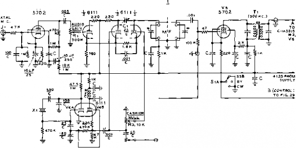 Ф CARRIER INSERT NOTES 1 - capacitors marked * are 240 jujuf for туре soob-31 model filter. 2- all resistors Гуг-шатт unless OrHERMflSE NOTED. 3-е- oijuf disc ceramic capacitor. 4- SUBMINIATURE TUBE SOCKET TER Ml NALS £702 eBS7 RED 5744 RED S1KC3HHC2P КС Н Н Р  CHASSIS 3  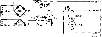 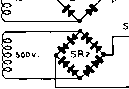 CONNECTIONS ТО CHASSIS 1 t. Z e.3V. -ill C+H2 (at each ruaesocket) Figure 26 SCHEMATIC, LOW FREQUENCY SECTION AND POWER SUPPLY OF SSB TRANSMITTER DLi-Time de/oy re/oy, 45 seconds, Amperife 6N045-T. ЫогпюПу open. Tl-455 kc. miniature i-f transformer. J. W. Miller 12-C9. Remove turns from windings to resonate at 500 kc. Ti-Г50 volt, 125 ma., SOO volt, 125 ma., 6.3 volt, 4 amp. Two 115 volt, 50-60 cycle primary windings. Walgren 3266. Walgren Electric Mfg. Co., Pasadena, Calif. CH СНг- 2 henry at 130 ma. Sfoncor C-2303 SR,-four sificon rectifiers. Max. inverse volts = 280. Sarfies-Tarzian M-500 or 1Ы1084 SR,-Eiglit sificon rect;/iers, two in series for eoch leg. Max. inverse volts - 280. Sarkes-Tarzian M-500 or 1N1084 MF-Callings Mechanical Filter, 3.1 kc. bandwidth, 500 kc. center frequency. Type 500B-31 Xi-Approximately 498 kc. Frequency chosen to place carrier oscillator at 20 db. down point on filter curve (see filter data sheet). RFC-2,5 mh. miniature r-f choke. Millen J300-2500. S,-See figure 29 Figure 27 INTERIOR OF LOW FREQUENCY PORTION OF FILTER TYPE SSB TRANSMITTER 500 kc. filter and low frequency components are on the bottom deck of the chassis. Small components are mounted between socket pins and miniature tie-point terminals. Interior shield isolates low frequency section from conversion oscillators and 4 Me. amplifier stages. The twenty meter conversion crystal Хз projects through the front panel of the transmitter (left). Note that transformers are mounted below chassis level to bring overall height even with that of miniature tubes. 6BK7A amplifier tube is also sub-mounted. Power leads that pass through Inter-stage shielding are routed through feed-thtu type ceramic insulators (Centralab type FT-1000),   an auxiliary supply for tuning operations, therefore, is highly recommended. Transmitter Loyout and Assembly The transmitter is built in three sections which are held together by a common front panel. The exciter (figure 27), the linear amplifier (figure 31), and the power supply (figure 33) make up these three sections. When the three sections are placed in position they appear as in figure 32. A rear view of the complete transmitter (minus the case) is shown in figure 28. The sections are bolted together and the complete assembly is fastened to the front panel. Because space is at a premium in such a configuration, each chassis is individually designed and shaped to fit the unusual layout. A sketch of the exciter chassis is shown in figure 24. It is formed from two sides and a base. The base mounts in a vertical position in the completed assembly (see figure 28). Side #1 of the exciter chassis contains the low frequency portion of the exciter and can be seen in figure 26, and the actual placement of major components is shown in figures 25 and 27. The mechanical filter occupies the upper right portion of the deck. Input and output circuits of the filter are isolated by a shield parthion that passes across the midsection of the filter. This shield also braces side #1 to the interior full-length shield seen in figure 27. Power leads from this portion of the exciter pass through .001 niiid. Centralab type FT ceramic feed-through capacitors. These capacitors are employed wherever power leads pass through an interstage shield. Note that coupling transformer Tl is submounted to bring its height in line with that of the sub-miniature tubes. All components are mounted on this side of the chassis and it is wired before it is attached to the base. Side #2 of the exciter chassis is attached to the base, and is further braced to side #1 by an end plate and an interstage shield. The 6BK7A socket, and transformers Ta and Тз are submounted to bring their height down to that of the sub-miniature tubes. The compon- 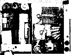 ii:e;*: :i :*:*e:iii> e:ii: : ? *#*.*; i l  Figure 28 REAR VIEW OF ASSEMBLED SSB TRANSMITTER The three sub-assemblies ot the transmitter are fastened together and bolted to the front panel. At the left is the power supply section. The a.c. power receptacle is at the bottom of the assembly with the two filter chokes at the left. Above the chokes is the bank of silicon rectifiers with the two voltage regulator tubes and dropping resistor at the top of the supply. The linear amplifier comprises the center section of the assembly. Antenna and receiver coaxial receptacles are mounted on a small bracket bolted between the outer sections. Plate coil is visible at the top of the chassis with adjustable loading switch to the tight. The right section of the assembly is the exciter, shown in detail in figure 27, SIDE # 2 OF CHASSIS 1 6BK7A Lz 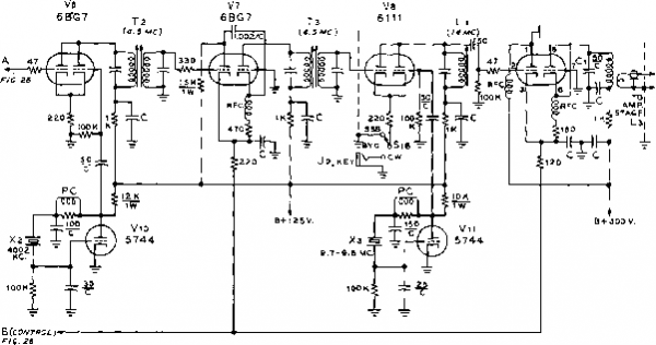 6524 PC CHASSIS#a l3 (1чмс) TO La S 4pC Yt\ £0 LA rfce  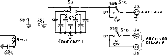 -iW- NOTES i - ЛЛ RES/STORS lyZ WATT UNLESS OTHERWISE NOTED. г.-С = .OILIR CERAMIC CAPACITOR 3-SEE FIGURE 26 FOR SOCKET CONNECTIONS OF SUBMINIATURE TUBES. 37.5 V.- ~ +300 V. +475 V. Figure 29 Tl, Tj-4.5 Mc. interstage transfarmer. J. W. Miller 6204 L,-20 turns #22 е., У4 diam.. 3/g long on ceramic farm with iron slug. J. W. Miller 4504 Lt, Ll-/5 turns #78, diam, long on polystyrene form. Linfc - 2 turns hookup wire. Li-12 turns#16, V/4 diam., V/2 long Cl-50 ii/ifd. ceramic trimmer. Centralab 822-АЫ Ci-50 ti/ifd. Johnson 50K10 Ca-9 iitifd. Johnson 9M11 Ci-50 iiiifd. Johnson 50L/5 Cs-75 ifd. fixed capacitor. Switch St adds seven 33 iдfd. capacitors in succession. (El-Menco type CM-/9 or Centralab TCZ-33). S,A-S-5 pole, 3 position. Centralab PA-201S 5t-Centralab P-121 Index Assembly with PIS progressive shorting deck. Xl-4002 kc. Precision Crystal Lab., Santa Monica, Calif. Хз-Frequency = 20 meter frequency minus 4500 kc. PC-Parasitic choke. 52 ohm, 1 watt resistor wound with 6 turns # Г6 wire. RFC-21/2 mh. miniature r-f choke. Millen J300-2500 M-0-70 d.c. milliammeter. Bi-37.5 vofts. Burgess XX22 plus two type Z flashlight cells Sff,- 750 ma. shunt. 100 ohms RFCi-Ohmite Z-74 r-f chofce ents are mounted and wired before the side is attached to the base. The base contains no wiring, except for two leads to the receiver disabling jacks J4 and Js. Amplifier chassis #2 occupies the center portion of the transmitter assembly, and can be seen in figures 23, 25, and 30. The tube socket and major parts are mounted on a flat plate, with the grid circuit components enclosed in a step shaped box. This shield is Figure 30 LINEAR AMPLIFIER AND EXCITER SECTIONS OF SSB TRANSMITTER Left; Linear antplifier is constructed upon an aiuminum sheet with grid circuit enclosed by small LShaped shield box. Low impedance link ieads from exciter pass througfi grommet in box. The coaxial oatput cable passes through chassis hole to changeover switch. Space to the right ot grid enclosure is occupied by meter and time delay relay. Right: Front view of assembled exciter chassis shows main panel controls. Chassis mounts in vertical position in final assembly. Twenty meter conversion crystal socket is at top, left, Of front of assembly. 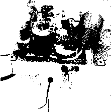  clearly visible in figure 32. The clearance space provided by the step is occupied by the SSB- standby-CW switch Si which is mounted to the panel in close proximity to the grid circuit components of the amplifier stage. The important leads to the control switch pass out of the grid compartment through ceramic feed through capacitors mounted on the wall of the step shield. The coaxial r-f output lead and the grid bias lead also pass through this shield and may be seen in figure 32. Figure 31 provides a close-up of the interior section of the amplifier chassis. Grid coil Ь is affixed to a polystyrene insulator and is mounted to the side of the chassis-box. Neutralizing capacitor Сз is placed on a small polystyrene plate adjacent to the 6524 amplifier tube. Plate r-f choke is next to Сз, and the 5KV plate blocking capacitor is supported between the top end of the choke and the stator of tuning capacitor Ci. The plate inductor L4  occupies the far end of the chassis. Pi-network switch Si; is placed next to the tuning capacitor, and the various padding capacitors are mounted directly on the back of the switch section. Power supply chassis #3 is attached to the front panel, and the weight of the supply is supported by a sheet metal screw run through the rear of the case into the supply chassis after final assembly. The power supply components are mounted upon a phenolic board which in turn is fastened to the aluminum chassis frame. The silicon rectifiers are held in position by fuse clips mounted on the boards and are placed so that they obtain the maximum possible ventilation. The primary power plug is placed on the rear of the supply chassis and projects through a hole cut in the case of the transmitter. The time delay relay DL-1 is mounted on the side of the amplifier chassis and may be seen in figure 31. The small bias battery for the amplifier stage fits below this space. Transmitter It is Important that no low Wiring frequency energy pass around the mechanical filter as spurious Figure 31 INTERIOR VIEW OF LINEAR AMPLIFIER GRID COMPARTMENT rime delay relay is mounted on side of grid box, occupying space between the panel meter and plate tank assembly. The grid coil and tuning capacitor can be seen below the tube socket. Neutralizing capacitor ii made from Johnson 30M8 with every third plate removed, but capacitor listed in parts list of figure 29 is satisfactory. 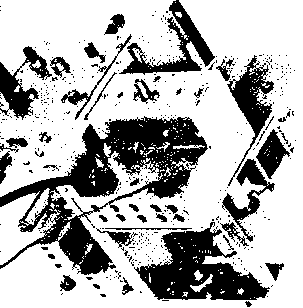 leakage will deteriorate tlie sideband and carrier suppression to a great degree. Power leads are therefore bypassed with feed through type ceramic capacitors at each partition. Several circuits (V,B, V=, V.1, v., and V ) are of the hot cathode type in which r-f voltage appears on the cathode of the tube. It is very necessary, therefore, to bypass the filament lead of these tubes to prevent a signal leakage path along the common filament wiring. Bypass capacitors are placed directly at the tube socket pins to conserve space and all wiring is short and direct. Coil Li (14 Mc. mixer plate coil) is mounted within the chassis assembly on a small bracket and a short extension shaft is soldered to the slug to permit circuit adjustment from the front panel. All wiring must be checked for opens, shorts, transpositions, and accidental grounds before power is applied to the transmitter. Testing the The transmitter should be test-Transmitter ed in sections before it is assembled in the case. The use of an auxiliary power supply is recommended. The exciter section should be tested first. A one kilocycle audio signal of low harmonic content is applied to the microphone jack Ji. Carrier insert potentiometer R-. is set at 2ero (ground end) and the antenna of a receiver capable of tuning to 500 kc. is attached to point A, figure 26. Before the audio signal is applied, carrier null potentiometer R,; and neutralizing capacitor Ci are adjusted for minimum signal at the crystal frequency of 498 kc. When the audio level is advanced an unmodulated carrier should be heard in the receiver. The frequency of the carrier will be Figure 32 COMPLETE R-F ASSEMBLY OF 20 METER SSB TRANSMITTER The two r-f units are bolted together in this view. The power supply chassis mounts on the right-hand edge of this assembly. Bias batteries fit in the lower area of the center unit, while plate meter fits into upper space in front of time delay relay. Compare this view with figure 23. This photo is taken from the right front, looking upward at the assembly. the crystal frequency plus the frequency of the audio signal, (i.e.; a 2 kc. audio signal will produce a carrier frequency of 500 kc). The carrier may be observed on an oscilloscope as described in chapter 17 and audio signal level and null adjustments are varied to reduce the residual ripple modulation of the carrier. Conversion crystal Хз and tubes Ve, V?, Vs, and Vio are inserted in the proper sockets and the receiver is tuned to 4.5 Mc. and coupled to the secondary winding of Tn. Transformer Tl, T=, and Тз are adjusted for maximum sig- 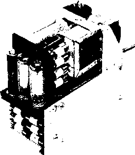 Figure 33 COMPACT SILICON POWER SUPPLY RUNS ENTIRE TRANSMITTER Miniature silicon rectifiers permit the complete power supply to be built in extremely small space. Rectifiers are mounted in fuse clips bolted to phenolic board. Power transformer occupies Imttom area of assembly and is fastened to aluminum assembly plate by the four bolts in the foreground. Primary power plug can be seen at top of unit, with ihe two filter chokes mounted back-to-bacf( on an arm of the assembly plate. Voltage regulator tubes and dropping resistors are in the foreground. Figure 34 DUPLEX TRANSMITTER-RECEIVER FOR 220 MC. RADIO LINK The width of the amateur 220 Mc. band permits simultaneous duplex transmission between two remote points. This compact Vfif package contains a complete 220 Mc. Radio Link. A crystal controlled transmitter operates on 224.6 Mc. The receiver operates at a frequency of 220.1 Mc. Signal from the transmitter acts as local oscillator for the i-t signal of 4.5 Mc. The complete station is housed in single steel cabinet. Transmitter section is at left with crystal mounted on panel. Receiver section is at right with power supply occupying lower portion of cabinet. Transmitter may be tone modulated for i.c.w. transmission.  nal level at 4.5 Mc. If a broadband oscilloscope, such as the Heathkit 0-11 is at hand, the signal may be observed visually and the audio level may be set for minimum carrier modulation. When monitored in the receiver the 4.5 Mc signal should be a pure carrier with little or no tone modulation. When audio gain control Rl is retarded, the signal should gradually weaken and disappear. After satisfactory operation is obtained at this frequency, crystal Хз and tubes Va and Vn are placed in their sockets. Capacitor Ci (figure 29) is tuned for maximum SSB signal in the 14 Mc. band. The interstage couphng transformers are peaked for maximum sideband signal and the receiver may be used for monitoring purposes. Voice modulation of the transmitter should be sharp and clean. The carrier may be inserted for test purposes by advancing potentiometer Ra. The next step is to check the operation of 220.1 MC, R-F AMP. Vi SAJiV R-F AMP. V2 M IXER v3 l-F 1 l-F 2 \ l-F #3 V6 224.SMC AMP. rRiPLER TRIPLER Vs OSC. Ve 24.994 MC. <вАв4)-
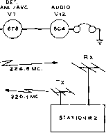 VHF RADIO LINK* MODULATOR Vl3 SPEECH Vl4 4J3-©- jCARBON -1-300 V. AT 210 MA. ICROPHONE RECT Vie (5ГЗ, 5Y3 1 1 RECT. Vl7 AUDIO OSC. V15 Figure 35 BLOCK DIAGRAM OF 220 MC. TRANSMITTER-RECEIVER Seventeen tubes are employed in the VHF station. The receiver has two grounded grid r-f stages for maximum sensitivity. Local oscillator injection is provided from the transmitter. Three 4.5 Mc i-f stages provide excellent gain and adequate selectivity.Transmitter is crystal controlled from 25 Mc. crystal and is plate modulated. Power supply provides 300 volts at 210 mtlliomperes. Transmitter draws 80 milliamperes, receiver draws 75 milliamperes, and modulator draws approximately 45 milliamperes under 100% modulation. Speech system is designated to be used with high gain mobile-type carbon microphone. 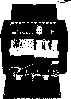 Figure 36 REMOVAL OF FRONT PANEL SHOWS PLACEMENT OF R-F CHASSIS The receiver and transmitter sections are bolted together ta form a single unit which sits near the top edges of the power transformer and modulator chassis. Power supply chassis is bolted ta cabinet on edge along left hand side, and modulator chassis is attached in the same fashion along the right hand side of the cabinet. Ventilation holes are drilled along upper edge of rear portion of cabinet. the linear amplifier stage. Bias voltage should be applied to the 6524 and meter switch Se set to the grid position. With full carrier insertion, one or two milliamperes of grid current will flow. The stage is neutralized by adjusting capacitor Ci for minimum grid current fluctuation as the plate circuit is tuned through resonance. A dummy load is then attached to the antenna receptacle (JO and the amplifier stage tuned in the usual manner. Make sure that plate voltage is never removed when excitation is applied to the tube as the screen current will increase to such a value as to endanger the tube. Always remove the screen lead when you remove the plate voltage. When the carrier is nulled out, the resting plate current of the linear amplifier will be about 20 тз., rising to about 100 ma. under voice peaks. No grid current should be indicated under these conditions. 28-5 A Duplex Transmitter-Receiver for 220 Mc Duplex operation is permitted in the 220 Mc. amateur band and opens interesting possibilities for unusual and novel forms of equipment. This class of operation consists of two one-way communication links separated in frequency from each other sufficiently to permit interference-free operation. The width of the 220 Mc. band permits placing one link at the low frequency end of the band and the other link near the high frequency end of the band without the danger of excessive interference between the links. Shown in figure 35 is the block diagram of a transmitter-receiver unit designed to serve as one end of a typical duplex communication link. Transmission takes place on 224.6 Mc, and reception takes place on 220.1 Mc- The frequency separation between the two links is 4.5 Mc At the opposite end of the link, transmission takes place on 220.1 Mc, and reception takes place on 224.6 Mc. The complete duplex station is built within a single cabinet and employs a common power supply. Separate antennas are used for transmission and reception, and communication is maintained in the same manner as in the case of a land-line, that is, simultaneous reception and transmission are possible. Transmitter-Receiver Circuitry The schematic of the transmitter - receiver is given in figure 37 and figure 38. The receiver section employs eight tubes in a superheterodyne circuit having two grounded grid r-f amplifier stages (figure 35). The intermediate frequency of the receiver is 4.5 Mc. and three stages of i-f amplification are used. Since the frequency separation of the two links is 4.5 Mc. it is feasible to employ the signal from the transmitter portion of the unit as the injection frequency for the first mixer of the receiver. Thus with the use of two properly chosen transmitter crystals (one at each end of the duplex link) the two transmitter-receivers are locked on frequency and tuning of the receivers is unnecessary. The transmission frequency at each end of the circuit controls the frequency of reception of the receiver portion of the transmitter-receiver. Two 6AJ4 tubes are used in the receiver as grounded grid r-f amplifier stages. The gain per stage is quite low but is sufficient to overcome the noise level of the mixer tube (V:i). R-f energy from the transmitter section pro- TRANSMITTER SECTION 6Aa4 (2<,994 KC.) RFCIc 4.7 К nsr TRANSMITTER COIL TABLE Ll-2eT., V2 D1A., 3/4 LONG. U2- 7 Т., 1/2 DIA 1/2- LONG. 1-3-2 Т., 1/2 DIA., 1/4 LONG. 1-4- 2T, 3/8 DIA., OVER l3. l S-2LONG, 1 WIDE, #10 WIRE L.6- 1 r. W12, 1 1/2 DIA. OVER LS. l 7- 1 ST. WIS, 1/8 DIA 3/4 LONG. 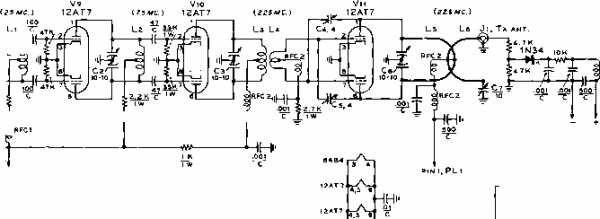 PIN 2, PLi NOTES 1 -ALL RESISTORS 1/Z WATT UNLESS OTHERWISE NOTED. 12AT7 TO METf R (.0-1 ОС ma.) RECEIVER SECTION R X ANT 6AJ4R-F V2 6AJ4R-F Jo JUAbTT Le 5ll.3.4,e.9t V3 (e.SMC.) 6AJ4 MIXER Tl MO с * PIN4, PIN3, PLi PLi (<.5MC.) T2 RECEIVER COIL TABLE (ALL COILS lya- DIA.) Le-3T. 1B,1/2 L.. ANT.TAPl 1/2,CATH.1T Le- 3T.#ie, 3/6 LONG, TAP 1 1/2 T. LlO-3T.#ie, 3/a LONG, TAP 2 1/4T. Ll1-2T.*ie, 3/e LONG. 6Тв OET/ANL  IRFC t i 2 e.2K 6.3 V. . TOPIN3, PLi B+RECEIVER Figure 37 SCHEMATIC, R-F SECTION OF TRANSMITTER-RECEIVER TRANSMITTER SECTION RECEIVER SECTION 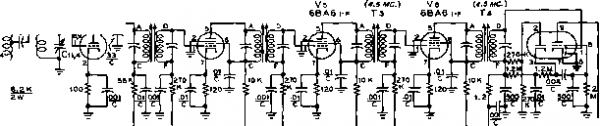 270 к 100 К -1лл*- PINS, PLi .01 . PIN e, PLi Cl, Сг, Сз, Cs-10-10 itiitd. Johnson 11MB11 Ci, Cs-4 fi/ifd. Erie 3139-E Cr-10 iiiifd. Johnson 9M11 RFCl-Ohmite Z-28 r-f choke f№Cr-Ohmite Z-23S r-f choke Xj-24,944 kc. crystal. Precision Crystal Lab., Santa Monica, Calif. Cs. C, Cio, Cn-i uufd. Erie 3139-E RtCi-Ohmite Z-235 r-f choke Ti-Ti-4.S Mc. interstage i-f transformer. J. W. Miller 1466 PLi-б contact receptocle. CIneh-Jones P-306-AB I2AU7 PTN 1 . PL 1 MODULATOR SECTION 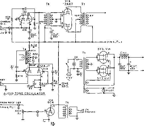 + 300 V. TO PI NS г i 5, PLi PI N 4, PL 1 POWER SUPPLY SECTION е.э V, TO pin 3, PL 1 NOTES \~all /lesiSTO/is 1уг tvArr unless otherwise noted. AUDIO VOLUME 10JUF -J- > RECEIVER 2S T RECEIVER AUDIO STAGE Figure 38 SCHEMATIC, AUDIO AND POWER SUPPLY SECTIONS OF TRANSMITTER-RECEIVER Ts, -70/C ptu, 4 ohm sec. Stancor A-3879 T -10K pri., Pri. to l/з see. = 2:7. Stancor A-4713 T? 70 pri., ак sec. Stancor A-384S Ti-360-0-360 vo/*s ot 200 ma., S v. at 6 amp., 6.3 v. at 9 amp. Stancor P-83S1 CH,-2 henry at 200 ma. Stancor C-2325 В-Miniature blower motor and fan, 7 75 vofts  11 w Figure 39 REAR VIEW, R.F DECKS OF TRANSMITTER-RECEIVER Receiver decfc is at the left and transmitter deck is at the right. The two chassis are bolted together to form one unit. Across the l>ack lip (left to right) are; Receiver antenna receptacle, pwoer plug PL meter terminals, transmitter antenna receptacle, and transmitter loading capacitor. Rows of Vi holes are drilled in the transmitter chassis to improve ventilation of the rectfier area under the chassis. 1 ... 56 57 58 59 60 61 62 ... 80 |
||||||||||||||||||||
|
© 2026 AutoElektrix.ru
Частичное копирование материалов разрешено при условии активной ссылки |