 |
 |
 |
| Главная Журналы Популярное Audi - почему их так назвали? Как появилась марка Bmw? Откуда появился Lexus? Достижения и устремления Mercedes-Benz Первые модели Chevrolet Электромобиль Nissan Leaf |
Главная » Журналы » Simple coaxial reflectometer 1 ... 64 65 66 67 68 69 70 ... 80 SPEECH AMPLIFIER 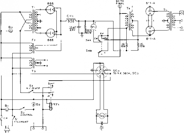 EXTERNAL 15 V.RELAY CONTROL Figure 10 SCHEMATIC, POWER SUPPLY AND MODULATOR DECK 7,-7775/7500 each side ct.. 625 mo., ICAS. 7 75/230 volt primary. Stancor P-8029 Гг-2.5 v., 70 a.. 10KV insulation. Stancor P-3060 Ts-6.3 v., 70 a. Stancor P-6308 -300 wott polypedance modulation transformer. Stancor Л-3898. Primary impedance 12K, secondary impedance 6K Ts- Polypedance driver transformer. Stancor Л-4762 RYi-DPDT relay, 70 ampere contacts, 7 75 v. a.c. coil Mi-0 - 500 mo. /Лг-0 - 700 mo. SiA-B-2 pole, 3 position high voltage switch. (Found in war surplus BC-306A antenna tuning unit), or equivalent CHi-500 mo. swinging cTiolce, 2-76 h. Stancor C-140S Bi-2-з-175 volt pilot lamps SOi-8 prong octal socket movable shorting bar are mounted at the B-plus end of the assembly. The rotor of the butter-fly capacitor is left floating and is panel driven through a high voltage shaft coupling. The neutralizing capacitors (Gi, GO are mounted on a triangular piece of polystyrene or other good insulating material and placed between the tube sockets. Construction of these capacitors is shown in figure 13. The 144 Mc. antenna link coil is a U-shaped pickup loop mounted beneath the linear tank circuit, while the 50 Mc. pickup coil is inserted between the turns of plate coil Lis. The single turn neutralizing coil Lu is placed near one end of Lis as shown in the photograph. Placement of the major components beneath the chassis may be seen in figure 6. The linear tank circuit LaA-B runs in zig-zag fashion from the plate terminals of the buffer tube Vs to two ceramic standoff insulators mounted on the bottom plate of the power amplifier enclosure. Spacing between the lines is held constant, and they are supported at the buffer end on two 1 ceramic insulators. The buffer tuning capacitor Ст is mounted to the chassis between the lines and panel driven with a phenolic shaft. The rotor of this capacitor is not grounded. The stators of Ci are connected to the lines with short lengths of flexible s.trap. Any grid current unbalance in the final amplifier stage can be corrected by varying the FIGURE 12 COIL CHART FOR 50-144 MC. TRANSMITTER Ll MC. COIL ) 36 T.#24 E., 1/2 DIA. MILLEN 690a6 FORM. l2-i50 MC. COIL ) 28T. 24E., I/2 DIA. MILLEN 69046 PORM. l3- 52 TURNS ге E. MILLEN 69046 FORM. La-2.ZT. CENTERTAP, 3/4 01 A., 32T.P.i. BiW iOli L5-15t. CENTER TAP, 1/2 DIA., 16T,p.l, BtW iOO LINK COIL: ONE TURN HOOKUP WIRE. Le- 2 1/2 T. CENTER TAP. 1/2 DIA. 16 T.P. i . BiW 3003 LINK coil; ONE TURN HOOKUP WIRE. l7- 7 T. CENTER TAP. Ъ/й' DIA 1вТ.Р BiW 3007 LINK coil: one TURN HOOKUP WIRE, l.i-{S0MC.) 7T, CENTER TAP, 3/4 DIA., в T.P. i. BSW 3010 LINK COIL : ONE TURN HOOKUP WIRE. t,144MC.)3 1/4X.02-X ,125 C0P.STRAP ВЫ1 U.iSEE FIS.7) LINK: 1 TURN HOOKUP WIRE BENT TO FIT La. L9A-B- n e COPPER WIRE, OR ,125 DIA, ROD, PLUS 3 OF 1/2 WIDE FLEXIBLE COPPER STRAP (eRWLEAO) PLUS 3/4 FLEXIBLE COPPER STRAP (PLATE LEAD ). ADJUST SPACING FOR RESONANCE, fff FIS. s FOP LAYOUT) LlO-ST., S/eDIA.,* ME. WIRE. ADJUST SPACING OF TURNS FOR RESONANCE AT 50 MC. WITH C7 AT FULL CAPACITY, LllA-B- 10 OF 1/в Х 1 1/a ALUMINUM STRAP, SPACED 3 3/8 CENTER TO CENTER, SHORTING BAR MADE OF SAME MATERIAL, ATTACHED 6 7/8 FROM PLATE END TO CENTER OF BAR. PLATE PIN RECEPTACLES REMOVED FROM SOCKET AND ATTACHED TO ENDS of LINES (SEE FISUPE 5 ) SOMC. COIL) 6 Т., 1 1/4 Dia. 6 COPPER WIRE, OR .125 TUBING. SPACE TURNS TO RESONATE TO 50 MC. WITH CSNEAR FULL CAPACITY. Ll3-19 CF#12E.W1RE BENT TO U SHAPE TO FORM 5 X 2 LOOP WITH 3 1/2 LEADS. PLACE UNDER Ll1 A-B. L14-1TURN, 2 DIA., 10 KV HOOKUP WIRE, Ll5-1 TURN, 1/2 DIA. 16E WITH INSULATED SLE EV ING. PLACE AT CENTER DF LlO. Lie-2 TURNS, 1 1/4 DIA lOKV HOOKUPWIRE. 6-32 bolt position of tlie taps on the lines until balanced current is obtained. The tuning range of the capacitor on 144 Mc. is reduced by moving the taps closer to the electrical center of the line. An L -shaped shield plate passes around the edge of tripler capacitor C4-C5 to shield the low power stages from the buffer plate lines. The under-chassis shielding is completed when a bottom plate is bolted to the chassis. The power supply section occupies the rear portion of the chassis. High vokage rectifiers Di-2-3-4 are mounted above the deck (figure 4) and the diodes of the bias supply are mounted below the chassis. Figure 9 shows the interior of the VFO compartment. The two oscillator coils are mounted on the side of the box, across from the four crystal sockets. The trimmer capacitors are mounted above their respective coils. The grid and cathode leads to oscillator tube Vi pass through a large rubber grommet mounted in the bottom of the enclosure. The Power and Moduiotar Deck The power supply is mounted upon a steel chassis measuring 13 x COPPER STRAP LEAD TO PLATE COPPER STRAP LEAD TO GRID poltstyrene sheet chassj5 6-32 BOLT A- 3/8 X 2- CERAMIC INSULATOR, TAPPED AT EACH END FOR e-32 MACHINE SCREWS, B,C-1 1/6 DIA, BRASS DISC WITH 3/6 CLEARANCE HOLE FOR CERAMIC INSULATOR, LOWER DISC SUPPORTED ON 3/6 CERAMIC INSULATORS. USE FLAT HEAD SCREWS. D- 3/6 CERAMIC INSULATORS, E- 1 1/6 DISC MADE OF TWO LAYERS OF ,015 THICK TEFLON HELD ATOP С BY CELLOPHANE TAPE. F- TWO 6/32 NUTS PLACED UNDER STRAP, STRAP AND NUTS SOLDERED TO BRASS PLATE. HOLE in PLATE PASSES e/32 BOLT. Figure 13 CONSTRUCTION OF NEUTRALIZING CAPACITOR FOR 826 STAGE Two capacitors are required (Cn and Си). Capacitors tiave top brace plate made of polystyrene sheet or other good VHF insulating material, Plate is supported on two ceramic insulators which form center support for capacitors. Plates of neutralizing capacitors are made of brass discs. The grid disc is supported on short ceramic insulators, and the plate disc is supported trom the polystyrene plate by 6-32 machine screw. Plate encircles ceramic insulator with a close fit. Plate lead and two 6-32 nuts are soldered to top plate. Mounting screw passes through this assembly, and also through hole drilled in top plate. After capacitors have been adjusted, tap plate is cemented to center ceramic insulator with clear nail polish to retain adjustment. 17 X 3 , as shown in figure 11. The modulator and rectifier tubes are placed near the front panel, with the modulation transformer and power transformer to the rear of the chassis. The swinging choke is placed between the tubes at the front-center of the chassis. Smaller components are mounted beneath the chassis. High voltages are applied to the transmitter by primary relay RYi, controlled by switch Ss and an optional external relay control circuit. Transmitter The tuned circuits of the trans-Adjustment mitter can be set to their proper operating range with the aid of a grid-dip osoillator. All r-f tubes must be in their sockets. Coil Ls is set to 8.5 Mc, and circuit C2-L4 is adjusted to 17 Mc. with C2 set at half-capacity. The 7 fifj-id. trimmer 7�53 capacitor across Le is adjusted to resonate the plate circuit of the first tripler stage to 50 Mc. with Сз at half-capaoity, and Cs-L? is tuned to the same frequency in the same manner with 50 Mc. plug PL-1 placed In socket SO-1. The grid coils of the buffer stage are next adjusted to frequency. The next step is to adjust the plate circuit of the buffer stage. Coil Lio is attached to the transmission line about 2 from the feed-through terminals, and capacitor Ct is tapped on the line about 1 closer to the buffer tube than is the coil. Resonance of the lines can be adjusted by changing the length of the flexible plate leads to the buffer tube, by varying the spacing of the lines, or by changing the spacing between the chassis and the lines. The tuning range of C? may be varied by shifting the position of the taps on the lines. Coil Lio is placed at the cold point of the line, which may be found by touching the line with a pencil lead when the transmitter is operating. Place the coil at the spot on the line that has the least fire when the transmitter is operating on 144 Mc. As soon as grid current can be measured on the power amplifier, the stage may be neutralized. The transmitter is first neutralized on 144 Mc. by adjusting capacitors Cn and Cia. The B-plus lead should be removed for this operation. Operating frequency is then changed to 50 Mc. and link coils Li4 and Lis are adjusted for complete neutralization on the six meter band. The 144 Mc. neutralization should then be rechecked. The links have very httle effect at 144 Mc, since the shorting bar effectively removes L12 and Lu from the circuit. However, the adjustment of the capacitors affects the setting of the 50 Mc. links, so the latter must be readjusted after each change in the settings of Cn and C12. Reduced voltage is now applied to the amplifier stage and it is loaded into a suitable antenna system. The links of coils Ls, Lc L?, and Ls should be adjusted for maximum grid drive. Loose coupling should be used as overcoupling reduces excitation to the power amplifier and results in double tuning of the stages. Buffer plate current runs about 100 milliamperes, and each amplifier tube should develop approximately 35 milliamperes of grid current. The 144 Mc. antenna link (Lis) is adjusted by varying the length of the loop and its position to the lines. It is mounted beneath the lines and spaced about away from them. Fine antenna loading may be controlled by loading capacitors С and Сю. The amplifier may be loaded to 200 ma. for phone operation, or 250 ma. for c.w. operation. The overall amplifier efficiency is better than 50%, delivering 160 watts to a dummy load with a power input of 300 watts at 144 Mc. Efficiency is better than 60% at 50 Mc. Modulator plate current rises to about 150 ma. on peaks for 100% modulation of the final amplifier. 31-2 A De-Luxe Transmitter for the 3.5-29.7 Mc. Range Shown in this section is a de-luxe phone/ c.w. transmitter for operation in the 80, 40, 20, 15, and 10 meter amateur bands. The transmitter runs 500 watts input on c.w. and 375 watts input on phone, and is completely self-contained in two small relay racks as illustrated in figure 14. The r.f. section of the transmitter is designed to be virtually TVI-proof, and modern techniques such as speech Figure 14 DE-LUXE STATION FOR THE DX MAN employes VFO-controlled, bandswitching, Phone-CW transmitter running up to 500 watts. This compact, all-barid transmitter employs a 7094 tetrode in a pi-network amplifier, modulated by ail-As. Clickless, break-in keying is used for C.W., and speech clipping and limiting are employed for AM phone. Modulator and power supply are in the rack at left, and entire r-f section is In right-hand rack. High stability VFO ensures drift-free frequency control. Transmitter is designed for maximum harmonic suppression and is virtually TVI-proof 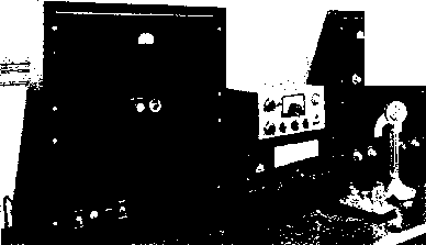 6 AC 7 6 AC 7 -(MULXJ- (3.SMC. ) С7, W.S, 7ЛМС.) ev7 I2AU7 12AX7 V9 SALS Vio 12AU7 Vn SSBl/eLS L.V.   7094 ANT, {3.5-30MC.) 811-A an-A AUDIO FILTER Vl7 Vie RECT)bV4-GB eee-A(RECT.)- (3.5-30 MC.y , V6 VTVM SALS JRECT,) eee-A POWER SUPPLY 115/230 V, Л, Figure 15 BLOCK DIAGRAM OF ALL-BAND 500 WATT TRANSMITTER R-t section employs bandswitching exciter tor coverage at TO, 75, 20, 40, and 80 meter bands. Variable frequency oscillator operates in 1.7 Mc. region to achieve maximum isolation. Tuning and antenna loading are aided by 6ALS vacuum tube voltmeter monitoring output of amplifier stage. Low level speech clipping and filtering, combined with high level audio filter imports punch to phone signal, yet holds sidebands to a minimum. Single high voltage supply powers modulator and final amplifier. clipping and clickless, break-in keying are incorporated in the transmitter. A high stability variable frequency oscillator is employed for frequency control, the dial of which is directly calibrated for each band. Band changing is a simple operation and may be accomplished in a few seconds. TransmiHer Circuitry and Layout A block diagram of the transmitter is given in figure 15. Nineteen tubes are used in the equipment: seven in the r-f section, six in the audio section, and six in the power supply. The RCA 7094 beam power tube is employed in the final amplifier stage. This compaa tube has high perveance and high power gain. It can be operated at full input to 60 Mc, and has a maximum plate dissipation of 125 watts. In addition, it has triple base-pin connections for the screen grid to permit good r-f grounding and large plate radiating fins for effective cooling. The compact size makes it especially effective in the high frequency portions of the communication spectrum. Driving requirements are modest and permit the use of a simplified bandswitching exciter.  Figure 16 VFO-EXCITER DECK CONTAINS ALL IMPORTANT OPERATING CONTROLS tow level r-f stages are built upon 8 xl7 x2 aluminum chassis. Keyer timing potentiometer Rj is at left, with excitation potentiometer Rl, control switch Si, and bandswitch Si in line, left ta right. VFO dial is centered on the panel. Output connector Pi is mounted on polystyrene plate atop shielded enclosure at riht. Shielding is made from Reynolds Do-it-yourself perforated aluminum sheet. г (I.7S- t.eSMC.) 120К Ll Cl сг 300 гоо %1ь -к ---- -сТ 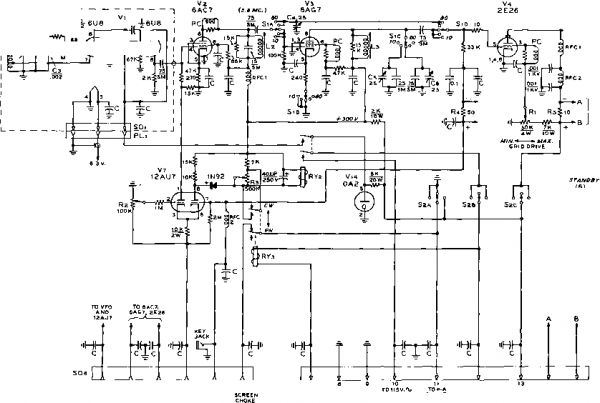 >TOSOs ТОНЕ <С) (А) ТЯА NSMIТ NOTES: \-Z-.0}JJF., eoo V. CERAMIC CAPACITOR. Z-ALi. RESISTORS 1-WATT UNLESS OTHERIVISE NOTED. 6.3 V. SCHEMATIC, EXCITER Ci-300 niitd. Bud CE-2008 dual bearing capacitor Cl-300 ttiitd. silYer mica capacitor. Vary tor desired frequency coverage. Сз-200O ii/itd. High accuracy capacitor, tolerance 1%, temperature coefficient zero, plus or minus 10 p.p.m. Centralab 950-202 Ci, Cs, Cs-25 fi/ifd. midget variable padding capacitor, ceramic L,-19 turns #20 e. wire, tapped S turns from ground end. Wound on ceramic form, W diam., 1 fiigA. Space the winding by interwinding #28 e. wire, therw remove. National XR-62 form, иг-30 turns #28 dsc. V2 diam., V2 long an National XR-50 form to St a iPHONE-CUl) Figure 17 DECK OF ALL-BAND TRANSMITTER 12 to pri. relay.RYa control ckt. 14 15 METER iSEE Pie. гз> L3--21 turns #22 е., Vl diam., V2 long on Nafionaf XR-SO form S,A-B-C-D-Two pole, 6 position decks (Centralab PA-3) with Centralab index assembly. StA-B-C-3 pole, 3 oosition rotary switch RYi-DPDT relay, 7.000 ohm d.c. coil RY,-DPDT relay, US-volt a.c. eoll PC-52 olim, 7-watt carbon resistor, wound with 3 turns #20 e. wire ЯГСт-2.5 mh. chofie National R-100 RtCt-VHF cfcoike, Ohmite Z-144 РА.ЗО1 С X 0> CD О D CL -I Q 3 <л On Ul ***JL &, BF OUTPUT ТОР-А > z О О 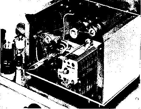 Figure 18 INTERIOR OF VFO SHOWING PLACEMENT OF MAJOR COMPONENTS The VFO is built upon two Va-i ch dural plates, one forming the base and the other iarming the front of the oscillatar enclosure. Inductor L, and padding capacitors are mounted to front wall, and the variable tuning capacitor is bolted to base. Oscillator tube (V-1) projects from far wall of enclosure ta remove as much heat from tuned circuit as passible. Entire VFO is mounted upon miniature shock mounts and dial is attached to VFO unit, rather than to rack panel. 6AG7 ond 2E26 tubes are at left, with 2C26 plate choke and SKY coupling capacitor in foreground. The variable frequency oscillator and exciter stages are built upon one chassis deck, as shown in figures 16, 18, 19, and 20. The complete schematic of this unit is given in figure 17. The variable oscillator covers the range of 1.75 Mc.-1.85 Mc, permitting full coverage of all amateur bands except the extreme top of the 28 Mc. band, and the top portion of the 80 meter band. Readjustment of the oscillator padding capacitor provides complete coverage of these segments, if desired. The VFO consists of a 6U8 pentode-triode (Vi) operating as a hot cathode oscillator and triode cathode follower. Extremely high-C is employed in the tuned circuit of the VFO to obtain a good order of stability. A 2000 fjifiid. precision ceramic capacitor Сз, forms the large portion of the tuning capacitance, and the coil Li is wound upon a ceramic form having a very low temperature coefficient. The cathode follower stage provides excellent circuit isolation for the oscillator, combined with a minimum of plate circuit loading. Figure 18 shows the layout of the major oscillator components. The circuit is built upon an 1/8 thick aluminum plate, bolted to a small panel of the same material. The sides, back, and top of the oscillator enclosure are made of aluminum sheet. The complete unit is mounted upon miniature rubber shock mounts. The VFO dial is firmly affixed to the enclosure and actually does not make physical contact with the panel at all. The frequency determining unit is thereby protected from jolts and jars which might cause a warble in the transmitter frequency. The r-f output from the cathode follower is 5 volts, r.m.s. Three tubes are employed in the multiplier and driver stages of the transmitter. The first 6AC7 doubler stage (V2) operates into a broadly resonant slug-tuned coil Ls. When tuning the exciter unit, this coil is peaked at 3.6 Mc The stage will then deliver substantially constant output over the range from 3.2 to 4.0 Mc. The 2E26 stage (V*) operates as an amplifier on the 3.5 Mc. band and as a doubler on the 7 Mc. band, driven directly from the 6AC7 buffer-doubler.  Figure 19 REAR VIEW OF EXCITER DECK Multiplier tubes are in the foreground. Adjustment holes for the multiplier trimmer capacitors are On side of chassis, /i-inch angle stock is run around chassis and panel to form foundation to which the perforated enclosure ts attached. Keyer tube V? is placed In rear corner. Potentiometer Ri and auxiliary key jack are on chassis wall below keyer tube. Short lead extends from 2E26 blocking capacitor up to connecting plug Pi mounted on enclosure.  Figure 20 UNDER-CHASSIS VIEW OF EXCITER All power wiring is run in stiielded braid, grounded to the chassis at convenient points. Voltage regulator tube Vu is mounted beneath the chassis on small angle brackets. RYs and RYs are mounted to the inner chassis wall, directly behind keyer panel control Rs. R-f circuits are at the opposite end of chassis, grouped around bandswitch Si. The slugs of coils Lt and Ls are adjustable from atop the chassis. Metal plate covers bottom of chassis to reduce spurious radiation from r.f. circuits. For operation on 20, 15, and 10 meters, switch SiD disconneas the 2E26 from the 6AC7 stage, and connects it to an auxiliary 6AG7 frequency multiplier (Va). The multiplier operates as either a doubler, a tripler, or as a quadrupler. Its output circuit, therefore, is either tuned to 7 Mc, 10.5 Mc, or 14 Mc. Coil Ls in the plate circuit of the 6AG7 resonates with residual circuit capacities to 14 Mc. Switch section SiC of the bandswitch adds additional capacity to lower the resonant frequency of this circuit to 10.5 Mc. or 7 Mc. The 2E26 stage operates as a doubler to 14 Mc, receiving 7 Mc. excitation from the 6AG7 stage. When the 6AG7 is tuned to 10.5 Mc, the 2E26 serves as a doubler to the 21 Mc. band. For 28 Mc. output from the 2E26, 14 Mc. excitation is received from the 6AG7 stage, and the 2E26 again functions as a doubler. Keying end A simpHfied schematic of the Control Circuit keying and control circuit for the exciter is shown in figure 21. A break-in type keyer is employed for c.w. operation. The unit is completely actuated by the transmitter key. When the key is pressed the transmitter is energized and may be keyed in a normal manner. The keyer holds the transmitter power supphes on while the key is manipulated. When the operator stops, the keyer turns off the transmitter after a short pause. Thus, the transmitter remains on between keyed characters and words, 15 к T 12AU7 V2 6АС7  RYz LL 2sk r2 V .10 к 2s0v. С--TO ZEZB bjT , [ key or Ml control grid -105 v. MOTES: RELAY CONTACTS RY3A NORMALLY OPEN-RELAY CONTACTS RY3B NORMALLY CLOSED. (SiA/zvAfoa.) PN.9 a S2B 7094 screen circuit (.SEE FIG. 2i) > t ,. switch Sa A = transmit В = standby С = tune .003 5 kv J RYs IK L IOMETER + 3 70 v- RYsbI о plate relay SOS ry4 pri. й-Э) swi -0-N-1,. MANUAL ll о AUTOMATIC \ (Sb IN POWER SUPPLY) Figure 2T KEYER AND CONTROL CIRCUITS Clickless, break-in keying is provided by this simple control circuit. See text for full details of operation 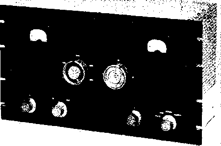 Figure 22 500 WATT POWER AMPLIFIER HAS SYMMETRICAL PANEL LAYOUT The 7094 amplifier stage Is enclosed in a separate deck. Plate milliammeter is at left, with 0-1 d.c. milliammeter at right which may be inserted in various power leads in exciter or amplifier. Large center knobs are (left) pi-network switch and (right) main amplifier tuning control. Controls across the bottom are (left to right): Pi-network loading capacitor, auxiliary pi-network capacitor switch, grid circuit tuning capacitor, and meter switch. Pi-networic switch Si is ganged with grid turret switch Ss eliminating one panel control. but will return to a stand-by position after the keying action has been completed. The turn-off time may be varied to suit the operators taste. For phone operation, the time delay circuit is eliminated, and the push-to-talk circuit actuates the keyer and control relays durealy. The whole sequence may be over-ridden and manual operation restored by means of a manual-automatic switch on the power supply chassis. Finally, a transmit - tune - standby switch S2A removes screen voltage from the final amplifier stage for tune-up purposes. Referring to figure 21, the sequence of operation is as follows: I-Key up, switch S2B on transmit. The right-hand section of the keyer tube Vi is cut off by the negative bias on the cathode. Potentiometer R2 is adjusted for 1 ma. current through 15K resistor to ground (-15 volts to chassis at point A). 6AC7 (v2) is cut off. 2-Key is depressed. Right-hand section of Vt conducts heavily and cathode voltage rises quickly, cutting off left section of Vi and removing blocking bias of 6AC7 (v2). Plate current of right-hand section of Vi operates RY2 and charges 40 ifd. capacitor through 1N92 diode. The relay closes, placing B-plus voltage on oscillator stage and operating the high voltage primary circuit relay circuit. This circuit may be rendered inoperative on standby position by switch s2b, enabling VFO to be used for frequency check or spotting purposes. 3-Key is released . Right-hand section of Vj cuts off immediately. Left-hand section draws 1 ma. and cuts off 6AC7 buffer tube. The 1N92 is back-biased by rise in 12AU7 plate voltage, keeping charge on 40 /хЫ. capacitor. Relay RY3 remains closed until capacitor is discharged through shunting resistances. Relay then opens, turning off high voltage supplies of transmitter. Release delay is controlled by potentiometer Ra. 4-Phone Operation Switch Si on modulator deck is closed for phone operation, placing the coil of relay RYa in tbe circuit. When the key is closed, or the press-to-talk circuit activated, RYA shorts out the time delay circuit of RY2, and at the same time RYsB removes a short across the screen modulation choke in the final amplifier. Exciter plate voltage is obtained from the modulator power supply (See Chapter 30, figure 17), and bias and amplifier voltage are derived from the main power supply, located on a separate chassis. The plate relay RY4 may be actuated by switch Sa or by the keyer circuit. TO EXCITER fgl. FIGUREI7 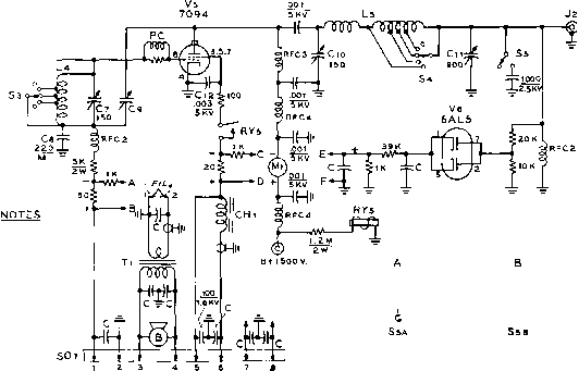 lANTENNA 1 - с = .00/, 00 И CERAMIC CAPACITOR. Z-ALL RESISTORS l-WATT UNLESS OTHERWISE SPECIFIED. CvA RFC4 -4. RFC4 JjD .00, Pl,oo, Figure 23 SCHEMATIC, 500 WATT POWER AMPLIFIER С-/50 tififd. Cs-220 /i/ifd., 7250 volt tixecf mica capacitor Сз-Disc-type rieutralizing capacitor. Natiorial ЫС-800 or equiva/ent. Ce-750 ii/ifd., 3000 volt. Johnson 150C30 Си-900 li/itd. Two gang broadcast capacitor (see text). Cii-Three .001, SKV ceramic capacitors. Centralab type 850. Place one capacitor on each screen terminal. Ц-Composed of two coi/s mounted on back ot S3 and connected in series. 80 meter coil: 28 turns, 1 diam., 1З/4 long. 40 meter tap at 18th turn from cold end. 20 meter coil: 7 turns, 1 diam., I/i long. IS meter tap at 4 turns, 10 meter tap at 3 turns from cold end. Adjust taps with grid-dip oscillator. Ls-Si-Sarfcer & Williamson #3850, 500 wott turret for 10-80 meters. S3-Single pole, 6 position ceramic switch, progressively shorting. Centralab PA-2042. RFCl-2.5 mh. choke. National R-100 RFC3-Heavy duty choke tor 3-30 Mc. range, SOO ma. Raypar RL-102 RFCi-VHF Choke, Ohmite Z-144, or equivalent PC-50 ohm composition resistor wound with 3 turns #20 e. Tl-6.3 vo/ts at 4 a. Stancor P-4019 CHi-7 Tl. at SO ma. Stancor C-1707 RYs-5PST sensitive relay, with 1 miiliampere d.c. coil Ml-0 - 500 d.c. milliammeter with insulated zero-set and bofce/ite cose. В-Small 11S-volt a.c. blower motor. The Amplifier The schematic of the ampli-Stoge fier is shown in figure 23, and various layout photographs are given in figures 22, 24, 25, and 26. Particular attention is given to TVI-reduction measures in the construaion of the unit. A single 7094 beam power tube is used in a pi-network circuit. The grid circuit (Li-Ct) is common to the plate circuit of the 2E26 and is capable of complete frequency coverage by victue of the tapped coil assembly shown in the under-chassis view. Bridge neutralization is employed to achieve maximum stability. Variable capacitor С and the grid bypass capacitor Cs form two legs of the bridge. To take advantage of the triple base-pin connections to the screen of the 7094 three separate low inductance bypass capacitors (Си) are used in the screen circuit, one attached to each of the screen socket terminals. A VHF parasitic choke (PC) is included in the lead to the control grid of the tube. As a result of these precautions, the amplifier is completely stable over the whole operating range. A sensitive relay RYs is incorporated in the screen circuit to protect the tube under conditions of low plate potential. The relay will open the screen circuit when the plate potential is removed from the amplifier stage. By far the most frequent type of damage to a tetrode tube is caused when full screen voltage is applied in the absence of plate voltage. The screen relay protects the tube from this type of damage. Self-modulation of the screen is accomplished by an iron core choke CHi in the screen circuit. This choke is shorted out by relay RYaB (figure 21) for c.w. operation. A pi-network configuration is used in the 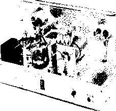 Figure 24 REAR OBLIQUE VIEW OF PI-COUPLED AMPLIFIER Dural angle strips are mounted around edge of 8 x77 x2 aluminum chassis and panel to which TVI enclosure is attached with self-tapping sheet metal screws. Meters are encased in aluminum cups, with r.f. filters mounted on fhe bock af each case. Meter leads are 10 KV teleYisian cable, enclosed in shielded braid. The 7094 tetrode is mounted at rear of chassis, with neutralizing capacitor Cs to left, and plate choke at right. Connections to plate of tube are made with flexible copper strap. Filament transformer is at left of chassis, with blower motor hidden behind it. Output capacitor of pi-network is below deck. plate circuit of the amplifier, employing one of the new Barker & Williamson 500 watt band-switching assemblies. A two-gang broadcast capacitor is employed for the low impedance output loading control. Switch Ss allows the insertion of an extra 1000 jit/ifd. capacitor for operation into low impedance loads at 3.5 Mc. The output circuit of the network is monitored by a 6AL5 vacuum-tube voltmeter (Ve) which may be employed during tune-up and loading adjustments. All power leads beneath the chassis are shielded in flexible braid, grounded at convenient points to the chassis. The meters are enclosed in spun aluminum cups that are bolted to the panel of the stage. Each meter lead is bypassed to the chassis with a .001, 5KV ceramic capacitor and a VHF cjioke is placed in series with the meter terminal. A small 115-volt blower motor is mounted at one end of the chassis (figure 25) to direct a coohng movement of air across the envelope of the tube. Placement of the major components beneath the chassis may be seen in figure 26. An aluminum partition separates the pi-network components from the tube socket and the grid circuit. The grid coil switch (Sa) is driven by means of a dial cord and drum from the plate bandswitch inductor shaft (Ls) atop the chassis. The cord passes through two holes in the chasisis deck. The main bandswitch control on the amplifier panel thus actuates both the grid and plate switches. Safety relay RYs is mounted on the rear apron of the chassis, and an aluminum plate covers the complete under-chassis area. A one-inch hole is cut in this plate directly below the stator terminal of grid tuning capacitor G, and a banana jack is mounted to a polystyrene plate bolted in place over the hole. This forms the low capacity input terminal, Ji. A mating hole is cut in the top of the exciter screen and covered with a second polystyrene plate having a banana plug mounted in the center. When the amplifier is slipped in the rack the plug and jack mate, forming the connection between the 2E26 plate and the tuned tank in the grid circuit of the final amphfier. Power Supply The power supply is built and Modulator upon a separate chassis, as shown in figure 27. Two 866A rectifier tubes are employed with a choke input filter to supply 1500 volts at 500 milhamperes for the r-f amplifier and modulator. Hash suppression chokes are placed in the rectifier plate leads to reduce the high frequency buzz sometimes super-imposed upon the carrier by mercury vapor tubes. Sufficient capacity must be used in the filter system to afford good dynamic stability to the supply under keyed loads, or under conditions 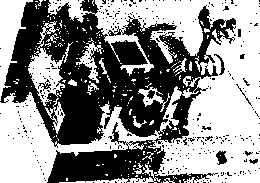 Figure 25 LEFT OBLIQUE VIEW OF PI-COUPLED AMPLIFIER Blower motor to coo/ 7094 tube is located between front panel and filament transformer. High yoltage and coaxial antenna terminals are on right of rear wall ot chassis. Addition of perforated screen makes enclosure radiation-proof. 1 ... 64 65 66 67 68 69 70 ... 80 |
|
© 2026 AutoElektrix.ru
Частичное копирование материалов разрешено при условии активной ссылки |