 |
 |
 |
| Главная Журналы Популярное Audi - почему их так назвали? Как появилась марка Bmw? Откуда появился Lexus? Достижения и устремления Mercedes-Benz Первые модели Chevrolet Электромобиль Nissan Leaf |
Главная » Журналы » Simple coaxial reflectometer 1 ... 66 67 68 69 70 71 72 ... 80 HANDBOOK Standard Circuits 691 о
 , fullvoltase volta half vatta<se ео=о.с O+=0. ii volts 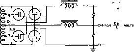 0 HALF AND FULL VOLTAGE BRIDGE POWER SUPPLY Тг (§) TWO VOLTAGE BRIDGE POWER SUPPLY 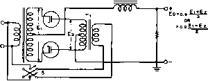
 0+ ео 0. -- © TWO TRANSFORMER POWER SUPPLY о о  Cl+Eo 0. %L 0+ео = о.> (Б) CENTER TAPPED METHOD FOR UNTAPPED TRANSFORMERS о => E -o+Eo0.0 e -о+ео-о. -- © TWO VOLTAGE POWER SUPPLY © SPECIAL FILTER CIRCUIT FOR BRIDGE RECTIFIER Figure 8 SPECIAL SINGLE-PHASE RECTIFICATION CIRCUITS A description of the application and operation of each of these special circuits is given in the accompanying text. is very small so that the peak-current rating of the rectifier tube seldom will be exceeded. The circuit of figure бВ is most commonly used in medium-voltage power supplies since this circuit is the most economical of filament transformers, rectifier tubes and sockets, and space. But the circuit of figure 6C, commonly called the bridge rectifier, gives bener transformer utilization so that the circuit is most commonly used in higher powered supplies. The circuit has the advantage that the entire secondary of the transformer is in use at all times, instead of each side being used alternately as in the case of the full-wave rectifier. As a point of interest, the current flow through the secondary of the plate transformer is a substantially pure a-c wave as a result of better transformer utilization, instead of the pulsating d-c wave through each half of the power transformer secondary in the case of the full-wave rectifier. The circuit of figure бС will give the greatest value of output power for a given transformer weight and cost in a single-phase power supply as illustrated. But in attempting to bridge-rectify the whole secondary of a trans- former designed for a full-wave rectifier, in order to obtain doubled output voltage, make sure that the insulation rating of the transformer to be used is adequate. In the bridge rectifier circuit the center of the high-voltage winding is at a d-c potential of one-half the total voltage output from the rectifier. In a normal full-wave rectifier the center of the high-voltage winding is grounded. So in the bridge rectifier the entire high-voltage secondary of the transformer is subjected to twice the peak-voltage stress that would exist if the same transformer were used in a full-wave rectifier. High-quality full-wave transformers will withstand bridge operation quite satisfactorily so long as the total output voltage from the supply is less than perhaps 4500 volts. But inexpensive transformers, whose insulation is just sufficient for full-wave operation, will break down when bridge rectification of the entire secondary is attempted. Special Single- Phase Rectification Circuits Figure 8 shows six circuits which may prove valuable when it is desired to obtain more than primary  © 6-PHASE BRIDGE i D.C.- TJTO---T-OfEo 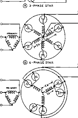 Eo = 1.17 Es Is =O.S77lD.C. RIPPLE FREQUENCY = 3F RIPPLE PERCENT - 18.3 PEAK INVERSE 2.09 EO TUBE VOLTAGE 2.44 ES O-EO Eo = 1.35 Es Is = 0.40 I d.c. ftlPPLE frequency = вР Ripple percent = 4.2 peak inverse . 2.09 EO tube voltage 2.83 Es Ш i d.c.-*. -O+Eo EO = 2.34 Es Is = o.eie I d.c. RIPPLE FREQUENCY =вр RIPPLE PERCENT = 4.2 PEAK INVERSE t.OS EO TUBE VOLTAGE - a.44 Es Figure 9 COMMON POLYPHASE-RECTIFICATION CIRCUITS These circuits are used when polyphase power is ayailable for the plate supply of a high-power transmitter. The circuit crt (B) is also called a three-phase full-wave rectification system. The circuits are described in the accompanying text. one output voltage from one plate transformer or where some special combination of voltages is required. Figure 8A shows a more or less common method for obtaining full voltage and half voltage from a bridge rectification circuit. With this type of circuit separate input chokes and filter systems are used on both output voltages. If a transformer designed for use with a full-wave rectifier is used in this circuit, the current drain from the full-voltage tap is doubled and added to the drain from the half-voltage tap to determine whether the rating of the transformer is being exceeded. Thus if the transformer is rated at 1250 volts at 500 ma. it will be permissible to pull 250 ma. at 2500 volts with no drain from the 1250-volt tap, or the drain from the 1250-volt tap may be 200 ma. if the drain from the 2 500-volt tap is 150 ma., and so forth. Figure SB shows a system which may be convenient for obtaining two voltages which are not in a ratio of 2 to I from a bridge-type rectifier; a transformer with taps along the winding is required for the circuit however. With the circuit arrangement shown the voltage from the tap will be greater than one-half the voltage at the top. If the circuit is changed so that the plates of the two rectifier tubes are connected to the outside of the winding instead of to the taps, and the cathodes of the other pair are connected to the taps instead of to the outside, the total voltage ouput of the rectifier will be the same, but the voltage at the tap position will be less than half the top voltage. An interesting variable-voltage circuit is shown in figure SC. The arrangement may be used to increase or decrease the output voltage of a conventional power supply, as represented by transformer Ti, by adding another filament transformer to isolate the filament circuits of the two rectifier tubes and adding another plate transformer between the filaments of the two tubes. The voltage contribution of the added transformer Тг may be subtracted from or added to the voltage produced by Ti simply by reversing the double-pole double-throw switch S. A serious disadvantage of this circuit is the fact that the entire secondary winding of transformer Тз must be insulated for the total output voltage of the power supply. An arrangement for operating a full-wave rectifier from a plate transformer not equipped with a center tap is shown in figure 8D. The two chokes Li must have high inductance ratings at the operating current of the plate supply to hold down the a-c current load on the secondary of the transformer since the total peak voltage output of the plate transformer is impressed across the chokes alternately. However, the chokes need only have half the current rating of the filter choke L2 for a certain current drain from the power supply since only half the current passes through each choke. Also, the two chokes Li act as input chokes so that an additional swinging choke is not required for such a power supply. A conventional two-voltage power supply with grounded transformer center tap is shown in figure BE. The output voltages from this circuit are separate and not additive as in the circuit of figure SB. Figure 8F is of advantage when it is desired to operate Class Б modulators from the half-voltage output of a bridge power supply and the final amplifier from the full voltage output. Both Li and L2 should be swinging chokes but the total drain from the power supply passes through Li while only the drain of the final amplifier passes through Ll. Capacitors Ci and C2 need be rated only half the maximum output voltage of the power supply, plus the usual safety factor. This arrangement is also of advantage in holding down the key-up voltage of a c-w transmitter since both Ll and L2 are in series, and their inductances are additive, insofar as the critical inductance of a choke-input filter is concerned. If 4 /xfd. capacitors are used at both Cl and C2 adequate filter will be obtained on both plate supplies for hum-free radiophone operation. Polyphase It is usual practice in commer-Rectification cial equipment installations Circuits when the power drain from a plate supply is to be greater than about one kilowatt to use a polyphase rectification system. Such power supplies offer better transformer utilization, less ripple output and better power factor in the load placed upon the a-c line. However, such systems require a source of three-phase (or two-phase with Scott connection) energy. Several of the more common polyphase rectification circuits with their significant characteristics are shown in figure 9. The increase in ripple frequency and decrease in percentage of ripple is apparent from the figures given in figure 9. The circuit of figure 9C gives the best transformer utilization as does the bridge circuit in the single-phase connection. The circuit has the further advantage that there is no average d-c flow in the transformer, so that three single-phase transformers may be used. A tap at half-voltage may be taken at the junction of the star transformers, but there will be d-c flow in the transformer secondaries with the power supply center tap in use. The circuit of figure 9A has the disadvantage that there is an average d-c flow in each of the windings. Rectifiers Rectifying elements in high-voltage plate supplies are almost invariably electron tubes of either the high-vacuum or mercury-vapor type, although selenium or silicon rectifier stacks containing a large number of elements are often used. Low-voltage high-current supplies may use argon gas rectifiers (Tungar tubes), selenium rectifiers, or other types of dry-disc rectification elements. The xenon rectifier tubes offer some advantage over mercury-vapor rectifiers for high-voltage applications where extreme temperature ranges are likely to be encountered. However, such rectifiers (3B25 for example) are considerably more expensive than their mercury-vapor counterparts. Peak Inverse Plate In an a-c circuit, the maxi-Voltage and Peek mum peak voltage or cur-Plate Current rent is V 2 or 1.41 times that indicated by the a-c meters in the circuit. The meters read the root-mean-square (r.m.s.) values, which are the peak values divided by 1.41 for a sine wave. If a potential of 1,000 r.m.s. volts is obtained from a high-voltage secondary winding of a transformer, there will be 1,410-volts peak potential from the rectifier plate to ground. In a single-phase supply the rectifier tube has this voltage impressed on it, either positively when the current flows or inverse when the current is blocked on the other half-cycle. The inverse peak voltage which the tube will stand safely is used as a rating for rectifier tubes. At higher voltages the tube is liable to arc back, thereby destroying or damaging it. The relations between peak inverse voltage, total transformer voltage and filter output voltage depend upon the characteristics of the filter and rectifier circuits (whether full- or half-wave, bridge, single-phase or polyphase, etc.). 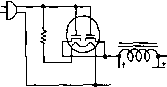 .LINE VOLTS-HEATER VOLTS HEATER AMPERES 0+ 0 LINE RECTIFIER T- T-0- =0----H-fw T- T o- SELENIUM NE-RECTIFIER L-l-T-. Ul © VOLTAGE DOUBLER FULL-WAVE c2-p 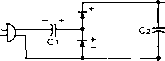 ® + VOLTAGE DOUBLER HALF-WAVE Cl J SELENIUM RECTIFIER VOLTAGE QUADRUPLER Figure 10 TRANSFORMERLESS POWER-SUPPLY CIRCUITS Circuits such as shown above are also frequently called line-rectifier circuits. Selenium rectifiers, vacuum diodes, or gas diodes may be used as the rectifying elements in these circuits. Rectifier tubes are also rated in terms of peak plate current. The actual direct load current which can be drawn from a given rectifier tube or tubes depends upon the type of filter circuit. A full-wave rectifier with capacitor input passes a peak current several times the direct load current. In a filter with choke input, the peak current is not much greater than the load current if the inductance of the choke is fairly high (assuming fuU-wave rectification). A full-wave rectifier with two rectifier elements requires a transformer which delivers twice as much a-c voltage as would be the case with a h4lf-wave rectifier or bridge rectifier. Mercury-Vapor The inexpensive mercury-vct-Rectifier Tubes por type of rectifier tube is almost universally used in the high-voltage plate supplies of amateur and commercial transmitters. Most amateurs are quite familiar with the use of these tubes but it should be pointed out that when new or long-unused mercury-vapor tubes are first placed in service, the filaments should be operated at normal temperature for approximately twenty minutes before plate voltage is applied, in order to remove all traces of mercury from the cathode and to clear any mercury deposits from the top of the envelope. After this preliminary warm-up with a new tube, plate voltage may be applied within 20 to 30 seconds after the time the filaments are turned on, each time the power supply is used. If plate voltage should be applied before the filament is brought to full temperature, active material may be knocked from the oxide-coated filament and the life of the tube will be greatly shortened. Small r-f chokes must sometimes be connected in series with the plate leads of mercury-vapor rectifier tubes in order to prevent the generation of radio-frequency hash. These r-f chokes must be wound with sufficiently heavy wire to carry the load current and must have enough inductance to attenuate the r-f parasitic noise current to prevent it from flowing in the filter supply leads and then being radiated into nearby receivers. Manufactured mercury-vapor rectifier hash chokes are available in various current ratings from the James Millen Company in Maiden, Mass., and from the /. W. Miller Company in Los Angeles. When mercury-vapor rectifier tubes are operated in parallel in a power supply, small resistors or small iron-core choke coils should be connected in series with the plate lead of each tube. These resistors or inductors tend to create an equal division of plate current between parallel tubes and prevent one tube from carrying the major portion of the current. When high vacuum rectifiers are operated in parallel, these chokes or resistors are not required. Transformerless Power Supplies Figure 10 shows a group of five different types of transformerless power supplies which are operated directly from the a-c line. Circuits of the general type are normally found in a.c.-d.c. receivers but may be used in low-powered exciters and in test instruments. When circuits such as shown in (A) and (B) are operated directly from the a-c line, the rec- HANDBOOK Standard Circuits 695 tifier element simply rectifies the hne voltage and delivers the alternate half cycles of energy to the filter network. With the normal type of rectifier tube, load currents up to approximately 75 ma. may be employed. The d-c voltage output of the filter will be slightly less than the r-m-s line voltage, depending upon the particular type of rectifier tube employed. With the introduction of the miniature selenium rectifier, the transformerless power supply has become a very convenient source of moderate voltage at currents up to perhaps 500 ma. A number of advantages are offered by the selenium rectifier as compared to the vacuum tube rectifier. Outstanding among these are the factors that the selenium rectifier operates instantly, and that it requires no heater power in order to obtain emission. The amount of heat developed by the selenium rectifier is very much less than that produced by an equivalent vacuum-tube type of rectifier. In the circuits of figure 10 (A), (B) and (C), capacitors G and G should be rated at approximately 150 volts and for a normal degree of filtering and capacitance, should be between 15 to 60 /xfd. In the circuit of figure lOD, capacitor G should be rated at 150 volts and capacitor G should be rated at 300 volts. In the circuit of figure lOE, capacitors G and G should be rated at 150 volts and G and G should be rated at 300 volts. The d-c output voltage of the line rectifier may be stabilized by means of a VR tube. However, due to the unusually low internal resistance of the selenium rectifier, transformerless power supplies using this type of rectifying element can normally be expected to give very good regulation. Voltoge-Doubler Figures IOC and lOD libs-Circuits trate two simple voltage-doubler circuits which will deliver a d-c output voltage equal approximately to twice the r-m-s value of the power hne voltage. The no-load d-c output voltage is equal to 2.82 times the r-m-s hne voltage value. At high current levels, the output voltage will be slightly under twice the line voltage. The circuit of figure IOC is of advantage when the lowest level of ripple is required from the power supply, since Its ripple frequency is equal to twice the line frequency. The circuit of figure lOD is of advantage when it is desired to use the grounded side of the a-c line in a permanent installation as the return circuit for the power supply. However, with the circuit of figure lOD the ripple frequency is the same as the a-c line frequency. OUTSIDE COLLECTOR INSIDE COLLECTOR  PHENOLIC WASHER BASE PLATE SELENIUM COAT-0 SELENIUM RECTIFIER CELL 100 90 80 # 70 60 50 40 30 20 10
® 100 160 200 250 RELATIVE LOAD CURRENT, PERCENT OP FULL. LOAD. Figure 11 THE SELENIUM RECTIFIER A-The selenium rectifier is a semi-conductor stack built up of nickel plated aluminum discs caated on one side with selenium alloy. В-Rectifier efficiency is high, reaching 70% for single phase service, dropping slightly at high current densities. Voltage The circuit of figure lOE lUus-Quadrupler trates a voltage quadrupler circuit for miniature selenium rectifiers. In effect this circuit is equivalent to two voltage doubiers of the type shown in figure lOD with their outputs connected in series. The circuit delivers a d-c output voltage under light load approximately equal to four times the r-m-s value of the line vohage. The no-load d-c output voltage delivered by the quadrupler is equal to 5.66 times the r-m-s line voltage value and the output voltage decreases rather rapidly as the load current is increased. In each of the circuits in figure 10 where selenium rectifiers have been shown, conventional high-vacuum rectifiers may be substituted with their filaments connected in series and an appropriate value of the line resistor added in series with the filament string. 32-4 Selenium and Silicon Rectifiers Selenium rectifiers are diaracterized by long life, dependability, and maintenance-free operation under severe operating conditions. The 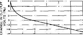 positive terminal contact negative terminal  0 50 100 1iO 200 250 300 LOAD CURRENT, PERCENT OF FULL СОЛО. Figure 12 VOLTAGE REGULATION OF SELENIUM CELL This graph applies to sinjf/e phase full wave bridge, and center-tap circuits which utilize both halves of the input wave. In single phase half wave circuits the regulation will be poorer. selenium rectifier consists of a nickel-plated aluminum base plate coated with selenium over which a low temperature alloy is sprayed. The base plate serves as the negative electrode and the alloy as the positive, with current flowing readily from the base plate to the alloy but encountering high resistance in the opposite direction (figure llA). This action results in effective rectification of an alternating input voltage and current with the efficiency of conversion dependent to some extent upon the ratio of the resistance in the conducting direction to that of the blocking direction. In normal power applications a ratio of 100 to 1 is satisfactory; however, special applications such as magnetic amplifiers often require ratios in the order of 1000 to 1. The basic selenium rectifier cell is actually a diode capable of half wave rectification. Since many apphcations require full wave rectification for maximum efficiency and minimum ripple, a plurality of cells in series, parallel, or series-parallel combinations are stacked in an assembly. Selenium rectifiers are operated over a wide range of voltages and currents. Typical applications range from a few volts at milliamperes of current to thousands of amperes at relatively high voltages. The efficiency of high quahty selenium rectifiers is high, usually in the order of 90% in three phase bridge circuits and 70% in single phase bridge circuits. Of particular interest is the very slight decrease in efficiency even at high current overloads (figure IIB). Threshold Voltage A minimum vokage is re-and Aging quired to permit a selen- ium rectifier to condua in the forward direction. This voltage, commonly known as the threshold voltage, precludes the use of selenium rectifiers at ex- siliconcell lspring Figure 13 THE SILICON CELL The common silicon rectifier is a pressure contact device capable of operation in ambient temperatures as high as ISCC. Heavy end ferrules that fit standard fuse clips are large enough to provide heat sink action. 7he positive ferrule is grooved to provide polarity identification and prevent Incorrect mounting. tremely low (less than one volt) applications. The threshold voltage will vary with temperature and will increase with a decrease in temperature. Under operating conditions, and to a lesser extent when idle, the selenium rectifier will age. During the aging period the forward resistance will gradually increase, stabilizing at a new, higher value after about one year. This aging will result in approximately a 7% decrease in output voltage. Voltage The selenium rectifier has ex-Regulation tremely low internal impedance which exhibits non-linear characteristics with respect to applied voltage. This results in good voltage regulation even at large overload currents. Figure 12 shows that as the bad is varied from zero to 300% of normal, the output voltage will change about 10%. It should be noted that because of non-linear characteristics, the voltage drop increases rapidly below 50% of normal load. Silicon Of all recent developments in the Rectifiers field of semi-conductors, silicon rectifiers offer the most promising range of apphcations; from extreme cold to high temperature, and from a few watts of output power to very high voltage and currents. Inherent charaaeristics of silicon allow junction temperatures in the order of 200° С before the material exhibits intrinsic properties. This extends the operating range of silicon devices beyond that of any other efficient semi-conductor and the excellent thermal range coupled with very small size per watt of output power make silicon rectifiers applicable where other rectifiers were previously considered impractical. Silicon The current density of a sili- Current Density con reaifier is very high, and on present designs ranges from 600 to 900 amperes per square inch of effective barrier layer. The usable current density depends upon the general construction of the unit and the abihty of the heat sink to conduct heat from the crystal. The small size of the crystal is illustrated by the fact that a rectifier rated at 15 amperes d.c, and 150 amperes peak surge current has a total cell volume of only .00023 inches. Peak currents are extremely critical because the small mass of the cell will heat instantaneously and could reach failure temperatures within a time lapse of microseconds. The assembly of a typical silicon cell is shown in figure 13. Operating The reverse direction of a sili- Characteristics con rectifier is charaaerized by extremely high resistance, up to 10 ohms below a critical voltage point. This point of avalanche voltage is the region of a sharp break in the resistance curve, followed by rapidly decreasing resistance (figure 15A). In practice, the peak inverse working voltage is usually set at least 20% below the avalanche point to provide a safety factor. The forward direction, or direction of low resistance determines the majority of power loss within the semi-conductor device. Figure 15B shows the static forward current characteristics versus applied voltage. The threshold voltage is about 0.6 volts. Since the forward resistance of a semi-conductor is very low, any unbalance between threshold voltages or internal voltage drop would cause serious unbalance of load distribution and ultimate failure of the overloaded section. A small resistance should therefore be placed in series with each half wave section  Figure 14 MINIATURE SEMI-CONDUCTOR TYPE RECTIFIER Raytheon CK-m power rectifier bolts to chassis to gain large heat sink area. Low internal voltage drop and high efficiency permit small size of unit. operating in parallel to balance the load currents. Some interesting and practical semi-conductor power supplies are shown in figure 16. Remember that the circuits of figure 16A and B, and those of figure 10 are hot with respect to one side of the power line. 32-5 100 Wott Mobile Power Supply High efficiency and compact size are the most important factors in the design of mobile power supplies. The power package described in this section meets these stringent require- ш u) ol ш > ш си (j Т 10 id:
о гь 50 75 100 125 150 PERCENT RATED PEAK INVERSE VOLTAGE ® (J Q fen b:z 50 U UJ Oir -5 UD ir< шо 0--! n
FORWARD VOLTAGE DROP i/OLTS, D.c. ® Figure 15 SILICON RECTIFIER CHARACTERISTICS A-Reverse direction of iiUcon rectifier is characteriied by extremely high resistance up to point of avalanche voltage, В-Threshold voltage of silicon cell is about 0.6 volt. Once device starts conducting the current increases exponentially with small increments of voltage, then nearly linearly on a very steep slope. I 17 V, 5 lOOiJF 60 JUF 100 juf: 250V. 450V. В * Dl -T e0UF л tSOMA, 450 V. (a) DUAL VOLTAGE DOUBLER WITH COMMON B-MINUS -0-285 V. 150 MA. 117V. 300 UF 2507. Dz D2 И- D3 1 \\ ► lloM. \ 150JJF ISOJJF OJJF L 250 V. У 450V. 50 V. ЛЛ a H,4S0 MA. 260 V. о о ?220V, О О 2S0V. Da Da D2;: OJUF + 250 V. Da! 0220 7. О Ог D2 5 so JUF row 250V De D2 10 w D2i к 2 50- D2 D2 -0+ieoov. 500 MA. eoxTF eoov. 80JUF 600 V. (в) HIGH CURRENT SUPPLY (C) 900 WATT HIGH VOLTAGE SUPPLY Figure 16 SEMI-CONDUCTOR POWER SUPPLIES A-Voltage quadrupler circuit. И point A is talten as ground instead of point S30 Yolts at ISO ma. from 115 volt a-c line. Supply is hot to line. В, supply will deliver В-Voltage tripler deliYering 325 volts at 4S0 ma. Supply is hot to line. С-900 watt supply for sideband service may be made from two voltage quadruplers working in series from inexpensive distribution-type transformer. Supply features good dynamic voltage regulation. PARTS LIST: Dl-Sarfces Tarzian Model ISO selenium cell or M€>del M-SOO silicon ceW. Dl-Sarkes Tarzian Model SOO selenium cell or Model M-500 silicon cell. Tl-Power distribution transformer, used backwards, 230/460 primary, 115/230 secondary, 0.75 KVA. Chicago PCB-247S0. ments, delivering 100 watts at various voltages to run both the mobile transmitter and receiver. The input power required by the supply is almost directly proportional to the output power drain, and only a small amount of power is wasted to actuate the vibrator reeds. The large demand for efficient and powerful mobile radio equipment has led to the development of new heavy-duty, vibrator-type power supply components; these are used to advantage in this unique design. The Split-Reed The new spUt-reed dual-inter-Vibrator rupter vibrator overcomes the power capacity limitations of the older type vibrators. In addition, this vibrator permits the design of power supplies requiring no component changes for operation from either the 6- or 12-volt d.c. power systems with which most automobiles are equipped. Until recently, the majority of vibrator supplies have been designed around the synchon-ous type vibrator. A simplified diagram of such a vibrator is shown in figure ISA. One set of vibrator contacts switches the battery current alternately through two opposed primary windings of a transformer, thus inducing a square-wave a.c. voltage in the secondary. This a.c. secondary voltage is then rectified by a second set of contacts on the vibrator armature. The limitations of this circuit are low power handling capacity and the need to use a different number of turns on the transformer primary when the battery voltage is changed from six to twelve volts. In the split-reed vibrator (figure 18B), two sets of double-throw contacts are electrically isolated from each other. Each set has much greater current carrying capacity than the synchronous vibrator. However, a power transformer having two center-tapped primary windings is required. One set of contacts switches the d.c. power alternately between halves of one primary winding, and the other set simultaneously switches the other winding. Therefore, the primaries can be connected in parallel for 6-volt operation, or in series for 12-volt operation. No wiring changes are needed in the supply if the battery is properly connected to the power input terminals. The Selenium Rectifier System A selenium rectifier system is employed in this supply. Since the vibrator contacts open and close abruptly, the periodically in- Figure 17 100 WATT MOBILE POWER SUPPLY rfiis high efficiency ma-bile supply features 6 or 12 Yolt input, and will completely power both the mobile transmitter and receiver. 4S0, 300, and 240 volts are available. At right is control box for complete mobile system. Overall size at supply is only 6 x6 x6 .  terrupted voltage impressed on ttie transformer primary lias practically a square waveform. The secondary voltage also has nearly a square waveform as a result and thus the peak voltage on the rectifiers is only slightly higher than the average voltage of the waveform. This means that the rertifiers in a vibrator-type power supply can be operated on a square wave voltage close to their maximum peak inverse voltage rating, instead of considerably below this rating, as when a sine wave a.c. voltage is applied to them. Power Supply This power supply has three Circuit high voltage sections as shown in figure 19. The 250 volt receiver supply is shown in figure 19A, the 300 volt low voltage transmitter supply in figure 19B, and the 450 volt high voltage transmitter supply is shown in figure 19C. Note that each rectifier has two sections. The part numbers correspond to the markings shown in the complete schematic of figure 20. In the 250 volt circuit, the full transformer secondary voltage is applied to a full wave rectifier consisting of half of rectifiers SRi and SR2. These two rectifiers form a common portion of all three reaifier circuits. The junction of the two rectifiers is grounded and the positive 250 volt output is taken from the center-tap transformer lead. This is the opposite of the usual full wave reaifier circuit. The 300 volt d.c. output is obtained from a bridge rectifier circuit (figure I9B) consisting of one-half of SRi and SR2 in the ground legs, plus SRa in the two bridge legs from which the positive voltage is obtained. Another bridge rectifier circuit is employed for the 450 volt d.c. output, again with the SYNCHRONOUS VI BRATOR VIBRATOR TRANSFORMER 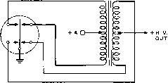 SPLIT REED VI BRATOR DUAL PRIMARY VIBRATOR TRANSFORMER 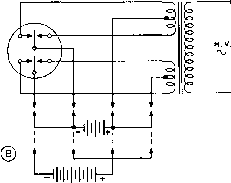 6 VOLT CONNECTIONS 12 VOLT CONNECTIONS Figure 18 SUPPLY FEATURES THE NEW SPLIT-REED VIBRATOR CAPABLE OF HANDLING 100 WATTS OF POWER AT EITHER 6 OR 12 VOLTS A-Simplified diagram of typical synchronous vibrator and rectifier circuit. В-Simplified diagram of typical split-reed vibrator and 6-12 volt d-c. changeover system. о с о о  SRiA SRea о 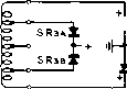 3 rSRiA SRZA о о 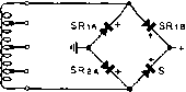 250 VOLT SUPPLY 300 VOLT SUPPLY 450 VOLT SUPPLY ® © Figure 19 SIMPLIFIED CIRCUITS OF RECTIFIER SYSTEMS USED IN HIGH EFFICIENCY MOBILE SUPPLY A-full wave, 250 volt rectifier. В-300 volt bridge circuit tapped across portion of the high voltage winding. C~4S0 volt bridge rectifier circuit. two grounded legs of the circuit passing through SRi and SR2. The other two sections of these rectifiers form the legs of the bridge from which the positive d.c. voltage is taken. Since there is little ripple voltage in the d.c. output from the rectifiers, a single 40 (lid. filter capacitor on the 300 volt section of the supply is adequate. Two 100 fiid. capacitors are placed in series across the 450 volt section and a capacitor input filter is employed for the low voltage section. The Canf-rol A push-to-talk power switch-Circuit ing circuit is included in the power supply so that the 250 volt output may be applied to a mobile receiver or converter. This is accomplished with one pair of contacts on a d.p.d.t. relay, RYi, which also turns on the 300 volt output to a transmitter exciter when its relay coil is energized. A second d.p.d.t. relay, RY2, turns on the 450 volt output to a transmitter final amplifier and modulator when its coil is energized. It also provides a power-reducing feature when the coil is not energized by applying 300 volts to the 450 volt output terminal and 250 volts to the 300 volt output terminal. Since all rectifiers have high voltage on them continuously when the supply is operating, the idling current flow through the unused rectifiers when receiving is reduced to almost zero by disconnecting them from the filter capacitors and bleeder resistors by the action of the relays. A special 20 volt secondary winding on the transformer provides transmitter negative bias through rectifier SR4 and a 50 /ifd. filter capacitor. Circuit Detdils- Low Voltage Section In this power supply, changing from 6- to 12-volt operation is accomplished with a 12-pin Cinch-Jones type 300 power plug and socket, Pi and Ji, respectively. A separate low voltage input cable is used for each voltage as shown in figure 20. Leads from Pi to the main power relay RYa should be made as short as possible to reduce the voltage drop. This is particularly important with a six volt power source, where a cable resistance of only 0.04 ohm will cause a one volt primary drop when the power supply is operating at full load. The six volt input plug conneas the alternate pairs of vibrator contacts and the halves of the transformer primary windings in parallel. These units are connected in series for twelve volt operation as shown in figure 18B. Six volts for the relay coils is supplied from the power cable through pin 6 on Ji. With the twelve volt plug, a voltage dropping resistor, Rl, is connected in series with the relay coils. If the power supply is to be operated exclusively from the higher primary voltage, relays having twelve volt coils should be used, thus eliminating Ri. There usually is sparking at the vibrator contaas so various capacitors and resistors are incorporated in the primary circuit to suppress any radio noise generated by vibrator aaion. These components are placed close to the pins of the vibrator socket. Component The heart of this power supply Ports is the vibrator transformer de- signed specially for two-way mobile radio equipment. It is readily available from many of the ЗООО General Electric Co. mobile radio service stations, or it may be ordered from the address given in the parts hst of figure 20. Power Supply All components except the Construction power transformer are enclosed inside a б хб хб aluminum utility box for maximum protection against dirt and dust. A sub-chassis made from 1/16- 1 ... 66 67 68 69 70 71 72 ... 80 |
||||||||||||||||||||||||||||||||||||||||||||||||||||||||||||||||||||||||||||||||||||||||||||||||||||||||||||||||||||||||||||||
|
© 2026 AutoElektrix.ru
Частичное копирование материалов разрешено при условии активной ссылки |