 |
 |
 |
| Главная Журналы Популярное Audi - почему их так назвали? Как появилась марка Bmw? Откуда появился Lexus? Достижения и устремления Mercedes-Benz Первые модели Chevrolet Электромобиль Nissan Leaf |
Главная » Журналы » Metal oxide semiconductor 1 ... 7 8 9 10 11 12 13 ... 91 dS(ON) 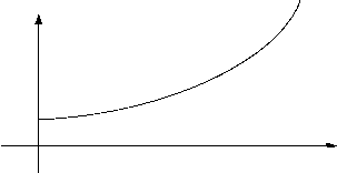 Drain Temperature FIGURE 6.25 The on-state resistance as a fraction of temperature, in high-voltage applications. The use of silicon carbide instead of silicon has reduced v DS(OW) many fold. As the device technology keeps improving, especially in terms of improved switch speeds and increased power handling capabilities, it is expected that the MOSFET will continue to replace BJTs in all types of power electronics systems. 6.7 MOSFET PSPICE Model The PSPICE simulation package has been used widely by electrical engineers as an essential software tool for circuit design. With the increasing number of devices available in the market place, PSPICE allows for accurate extraction and understanding of various device parameters and their varied effects on the overall design prior to their fabrication. Todays PSPICE library is rich with numerous commercial MOSFET models. This section will give a brief overview of how the MOSFET model is implemented in PSPICE. A brief overview of the PSPICE modehng of the MOSFET device will be given here. 6.7.1 Static Model There are four different types of MOSFET models that are also known as levels. The simplest MOSFET model is called the LEVELl model and is shown in Fig. 6.26. [9, 10]. The LEVEL2 model uses the same parameters as LEVELl, but it provides a better model for Ids by computing the model coefficients KP, VTO, LAMBDA, PHI, and GAMMA directly from the geometrical, physical and technological parameters [10]. LEVEL3 is used to model the short-channel devices and LEVEL4 represents the Berkeley short-channel IGFET model (BSIM-model). For the triode regions, Vq > У^, is < GS id DS < GS ~ Th the drain current is given by 2L-2X, (%S - Th - )DS(1 + DS) (6.41) Gate  Bulk(substrate) Source FIGURE 6.26 Spice LI MOSFET static model. In the saturation (linear) region, where Vq > id DS > GS ~ Th the drain current is given by Id = (Gs - Th)(l + ADs) (6.42) Where Kp is the transconductance and Xjj is the lateral diffusion. The threshold voltage is given by VTh = TO + д^2фр - VBs - у/щ) (6.43) where, Уро is the zero-bias threshold voltage; д is the body-effect parameter; and фр is the surface inversion potential. Typically, < L and Я 0. The term (1 + Ays) is included in the model as an empirical connection to model the effect of the output conductance when the MOSFET is operating in the triode region. Lambda is known as the channel-length modulation parameter. When the bulk and source terminals are connected together, that is, ys = 0, the device threshold voltage equals the zero-bias threshold voltage. where Уро is positive for the n-channel enhancement mode devices and negative for the depletion mode n-channel devices. The parameters Xp, Vq, S, ф are electrical parameters that can be either specified directly in the MODEL statement under the PSPICE keywords KP, VTO, GAMMA and PHI, respectively, as shown in Table 6.1. These parameters can also be calculated when the geometrical and physical parameters. The two-substrate currents that flow from the bulk to the source /gs and from the bulk to the drain 4 are simply diode currents and are given by 4s = 4s( -i) 4d = s( -i) (6.44) (6.45) Where /§3 and /j)s are the substrate source and substrate drain saturation currents. These currents are considered equal and given as in the MODEL statement with a default value of 10~ A. Where the equation symbols and their corresponding PSpice parameter names are shown in Table 6.1. In PSpice, a MOSFET device is described by two statements, with first statement starting with the letter M and the second statement starting with .Model, which defines the model used in the first statement. The foUowing syntax is used: m<device name> <drain node number> gat e n о de n umb e r > <source node number> <substrate node number> <model name> [<param l>=<value l> <param 2>=<value >....] .model <model name> <type name> [ (<param l>=<value l> <param 2>=<value 2> .....] Where the starting letter m in m<devic name> statement indicates that the device is a MOSFET and <device name> is a user specified label for the given device, the <model name> is one of the hundreds of device models specified in the PSpice library; and <model name> or the same name specified in the device name statement <type name>, is either NMOS of PMOS, depending on whether the device is n- or p-channel MOS, respectively. An optional list of parameter types and their values foUows. Length L and width W and other parameters can be specified in the m<device name>, in the .MODEL or .OPTION statements. A user may select not to include any value, and PSpice wiU use the specified default values in the model. For normal operation (physical construction of the MOS devices), the source and bulk substrate nodes must be connected together. In aU the PSpice library files, defauh parameter values for L, W, AS, AD, PS, PD, NRD, and NDS are included, and a user then should not specify such values in the device M statement or in the OPTION statement. The power MOSFET device PSpice models include relatively complete static and dynamic device characteristics given in the manufacturing data sheet. In general, the foUowing effects are specified in a given PSpice model: dc transfer curves, on-resistance, switching delays, gate dive characteristics, and reverse-mode body-diode operation. The device characteristics that are not included in the model are noise, latch-ups, maximum voltage, and power ratings. Please see OrCAD Library FUes. Example 6.3. Let us consider an example that uses IRF MOSFET and connected as shown in Fig. 6.27. It was decided that the device should have a blocking voltage (Уозз) 600 V and drain current of 3.6 A. The device selected is IRF CC30 with case TO220. This device is hsted in the PSpice library under model number IRFBC30 as foUows: library of power mosfet models copyright orcad, inc. 1998 all rights reserved. $revision: 1.24 $ $author: rperez $ $date: 19 october 1998 10:22:26 $ . model irfbc30 nmos nmos The PSpice code for the MOS device labeled SI used in Fig. 6.27 is given by msi 3 5 0 0 irfbc30 .model irfbc30 .model irfbc30 nmos(level=3 gamma=0 delta=0 eta=0 theta=0 kappa=0.2 vmax=0 xj=0 + tox=100n uo=600 phi=.6 rs=5.002m kp=20.43u w=.35 l=2u vto=3.625 + rd=1.851 rds=2.667meg cbd=7 90.1p pb=.8 mj=.5 fc=.5 cgso=1.64n + cgdo=123.9p rg=1.052 is=720.2p n=1 tt=685) int1 rectifier pid=irfcc30 case=to220 6.7.2 Large Signal Model The equivalent circuit of Fig. 6.28 includes five device parasitic capacitances. The capacitors Cq, Cq, and Cqj), represent the charge-storage effect between the gate terminal and the bulk, source and drain terminals, respectively. These are nonlinear two-terminal capacitors expressed as functions of W, L Cox, gs to ds Qbo gsO Qdo- Capacitors Cqq, Cqq, and Cqy)o outside the channel region, are known as overlap capacitances that exist between the gate electrode and the other three terminals, respectively. Table 6.2 shows the list of MOSFET capacitance parameters and their default values. Notice that the PSpice overlap capacitor keywords (Qbo C(3sO Qdo) proportional either to the MOSFET width or length of the channel as foUows:
capacitors are given by. gs - LwQ GD - wqx GB - GBO gs - ds - 2(%s - VTh(-ds/ + Qso- + GDO- (6.47) TABLE 6.1 PSPICE MOSFET parameters (a) Device dc and parasitic parameters
All superscript numbers in the Description column indicate that this/these parameter(s) are available in this/these level number(s), otherwise it/they are available in all levels. ® ® figure 6.27 MOSFET. Example of a power electronic circuit that uses a power where Kx is the oxide relative dielectric constant, Eq denotes the free-space dielectric constant as equal to 8.854 X 10~ F/m; and Tx is the oxide thickness layer as given by data in Table 6.1. Finally, the diffusion and junction region capacitances between the bulk-to-channel (drain and source) are modeled by and Qs across the two diodes. Because for almost aU power MOSFETS, the bulk and source terminals are connected together and at zero potential, diodes Dg and Dgg do not have forward bias, thereby resulting in very small conductance values, that is, smaU diffusion capacitances. The smaU signal model for MOSFET devices is given in Fig. 6.29. Example 6.4. Figure 6.30a shows an example of a softswitching power factor connection circuit that has two MOSFET. Its PSPICE simulation waveforms are shown in Fig. 6.30b. Table 6.2 shows the PSPICE code for Fig. 6.30a. In the saturation (hnear) region we have Cgb = Qbo (6.48) gd = gdo Where Qx is the per-unit-area oxide capacitance given by Cox=- 6.8 Comparison of Power Devices As stated earlier, the power electronic range is very wide, from hundreds of milliwatts to hundreds of megawatts and thus it is very difficult to find a single switching device type to cover aU power electronic apphcations. Todays available power devices have tremendous power and frequency rating range, as weU as diversity. Their forward current ratings range from a few amperes to a few kiloamperes, their blocking voltage rating Drain Gate 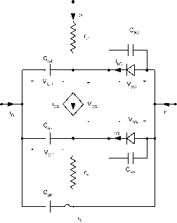 Bulk(Substrate) 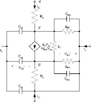 figure 6.28 Large-signal model for the -channel MOSFET. figure 6.29 Small signal equivalent circuit model for MOSFET. {Ts} TABLE 6.2 PSPICE MOSFET capacitance parameters and their default values for Figure 6.30a * source ZVT-ZCS D Do V Vs L Ls Kn Kl C Co V Vin L Li V Va {Ts} D Dp C C7 R Ro C C8 D Dao D Di L Lp2 C C9 L Las Kn K2 L Lpl L Lap C Cp2 C Cpl L Lak M M1 M M2 . PARAM D=0 N00111 OUT Dbreak N00105 9 DC 0 AC 0 PULSE 0.9.0.0.0 {DTs} 0 N00111 {n.l6} L Lpl L Lp2 L Ls 0.995 OUT 0 70uF IC=50 N00103 0 110 N00103 N00099 17.6u IC=0 N-109 0 DC 0 AC 0 PULSE 0 9 {-DeltaTs/1.1} 0 0 {2 . 0DeltaTs} N00121 N00169 Dbreak N00111 OUT 30p OUT 0 25 N00143 OUT lOp N00143 OUT Dbreak N00099 N00245 Dbreak N00121 0 {n} IC=0 N00169 N00121 lOp N00143 0 {0.4nl} L Lap L Las 1. 0 N00245 N00169 {n} IC=0 N00245 N000791 {nl} N00245 N00121 47u IC=170 N00169 0 47u IC=170 N000791 N000911 5u IC=0 N000911N00109 0 0 IRFBC30 N00245 N00105 0 0 IRF840 . 3 DELTA=0 . 1 Nl=400u N=lmH TS=2us MOSFET MODEL PARAMETERS
□ U(Ua:+) * U(US:+)  FIGURE 6.30 (a) Example of power electronic circuit; and (b) PSpice simulation waveforms. ranges from a few volts to a few kilovolts, and the switching frequency ranges from a few hundred hertz to a few mega hertz (see Table 6.3). This table compares the available power semiconductor devices. We only give relative comparison because there is no straightforward technique that can rank these devices. As we compile this table, devices are stiU being developed very rapidly with higher current, voltage ratings. frequency versus power, iUustrating the power and frequency ratings of available power devices. 6.9 Future Trends in Power Devices It is expected that improvement in power handling capabilities and switching frequency. Finally, Fig. 6.31 shows a plot of and increasing frequency of operation of power devices wiU TABLE 6.3 Comparison of power semiconductor devices
105- As power rating increases, frequency decreases  As frequency increases, power decreases 10 10 10 10 10 10 10 10 Frequency (Hz) FIGURE 6.31 Power vs frequency for different power devices. continue to drive the research and development in semiconductor technology. From power MOSFET to power MOS-IGBT and to power MOS-controUed thyristors, power rating has consistently increased by factor of 5 from one type to another. Major research activities will focus on obtaining new device structures based on MOS-BJT technology integration so as to rapidly increase power ratings. It is expected that the power MOS-BJT technology will capture more than 90% of the total power transistor market. The continuing development of power semiconductor technology has resulted in power systems with driver circuit, logic and control, device protection and switching devices being designed and fabricated on a single chip. Such power 1С modules are called smart power devices. For example, some of today s power supphes are available as ICs for use in low-power apphcations. No doubt the development of smart power devices will continue in the near future, addressing more power electronic applications. References 1. B. Joyant Baliga, Power Semiconductor Devices, PWS Publishing, New York, 1996. 2. Lorenz, Marz and Amann, Rugged Power MOSFET - A milestone on the road to a simplified circuit engineering, SIEMENS Application Notes on S-EET Application, 2000. 3. M. H. Rashid, Microelectronic Circuits: Analysis and Design, PWS Publishing, Boston: MA, 1999. 4. A. Sedra and K. Smith, Microelectronic Circuits, 4th Ed., Oxford Series, Oxford Univ Press, Oxford, 1996. 5. Ned Mohan, T. M. Underland, and W. M. Robbins, Power Electronics: Converters, Applications, and Design, 2nd Ed., John Wiley, New York, 1995. 6. Richard and Cobbald, Theory and Applications of Field Effect Transistors, John Wiley, New York, 1970. 7. R. M. Warner and B. L. Grung, MOSFET: Theory and Design, Oxford Univ Press, Oxford, 1999. 8. D. K. Schroder, Advanced MOS Devices, Modular Series on Solid State Devices, MA: Addison Wesley, 1987. 9. J. G. Gottling, Hands on pspice, Houghton Mifflin Company, New York, 1995. 10. G. Massobrio and P. Antognetti, Semiconductor Device Modeling with PSpice, McGraw-Hill, New York, 1993. Insulated Gate Bipolar Transistor S. Abedinpour Department of Electrical Engineering and Computer Science University of Illinois at Chicago, Illinois 6067 USA K. Shenai 851 South Morgan Street (М/С 154) Chicago, Illinois 60607-7053 USA 7.1 7.2 7.3 7.4 7.5 7.6 Introduction........................................................................................ 101 Basic Structure and Operation................................................................ 102 Static Characteristics............................................................................. 103 Dynamic Switching Characteristics.......................................................... 105 7.4.1 Turn-on Characteristics 7.4.2 Turn-off Characteristics 7.4.3 Latch-up of Parasitic Thyristor IGBT Performance Parameters................................................................ 106 Gate-Drive Requirements....................................................................... 107 7.6.1 Conventional Gate Drives 7.6.2 New Gate-Drive Circuits 7.6.3 Protection Circuit Models..................................................................................... 109 7.7.1 Input and Output Characteristics 7.7.2 Implementing the IGBT Model into a Circuit Simulator Applications........................................................................................ 114 References........................................................................................... 115 7.1 Introduction The insulated gate bipolar transistor (IGBT), which was introduced in the early 1980s, has become a successful device because of its superior characteristics. The IGBT is a three-terminal power semiconductor switch used to control electrical energy and many new applications would not be economically feasible without IGBTs. Prior to the advent of the IGBT, power bipolar junction transistors (BJTs) and power metal oxide field effect transistors (MOSFETs) were widely used in low to medium power and high-frequency applications, where the speed of gate turn-off thyristors was not adequate. Power BJTs have good on-state characteristics but long switching times especially at turn-off. They are current-controlled devices with small current gain because of high-level injection effects and wide basewidth required to prevent reach-through breakdown for high blocking voltage capability. Therefore, they require complex base-drive circuits to provide the base current during on-state, which increases the power loss in the control electrode. On the other hand, power MOSFETs are voltage-controlled devices, which require very small current during the switching period and hence have simple gate-drive requirements. Power MOSFETs are majority carrier devices, which exhibit very high switching speeds. Fiowever, the unipolar nature of the power MOSFETs causes inferior conduction characteristics as the voltage rating is increased above 200 V. Therefore, their on-state resistance increases with increasing breakdown voltage. Furthermore, as the voltage rating increases, the inherent body diode shows inferior reverse recovery characteristics, which leads to higher switching losses. In order to improve the power device performance it is advantageous to have the low on-state resistance of power BJTs with an insulated gate input similar to that of a power MOSFET. The Darhngton configuration of the two devices shown in Fig. 7.1 has superior characteristics as compared to the two discrete devices. This hybrid device could be gated in the same way as a power MOSFET with low on-state resistance because most of the output current is handled by the BJT. Because of the low current gain of BJT, a MOSFET of equal size is required as a driver. A more powerful approach to obtain the maximum benefits of the MOS gate control and bipolar current conduction is to integrate the physics of MOSFET and BJT within the same semiconductor region. This concept gave rise to the commercially available IGBTs with superior on-state characteristics, good switching speed and exceUent safe operating area. Compared to power MOSFETs the absence of the integral body diode can be considered as an advantage or disadvantage depending on the switching speed and current requirements. An external fast-recovery diode or a diode in the same package can be used for specific applications. The IGBTs are replacing MOSFETs in high-voltage applications with lower conduction losses. They have on-state voltage and current density comparable to a power BJT with higher switching frequency. Although they exhibit fast turn-on, their turn-off is slower than a MOSFET because of current fall time. Also, IGBTs have considerably less silicon area than similar rated power MOSFETs. Therefore, by replacing power MOSFETs with IGBTs, the efficiency is improved and cost is reduced. Additionally, IGBT is known as a conductivity-modulated FET (COMFET), insulated gate transistor (IGT), and bipolar-mode MOSFET. As soft-switching topologies offer numerous advantages over the hard-switching topologies, their use is increasing in the industry. By use of soft-switching techniques IGBTs can operate at frequencies up to hundreds of kilohertz. However, IGBTs behave differently under soft-switching condition compared to their behavior under hard-switching conditions. Therefore, the device trade-offs involved in soft-switching circuits are different than those in the hard-switching case. Application of IGBTs in high-power converters subjects them to high-transient electrical stress such as short-circuit and turn-off under clamped inductive load, and therefore robustness of IGBTs under stress conditions is an important requirement. Traditionally, there has been limited interaction between device manufacturers and power electronic circuit designers. Therefore, the shortcomings of device reliability are observed only after the devices are used in actual circuits. This significantly slows down the process of power electronic system optimization. However, the development time can be significantly reduced if aU issues of device performance and reliability are taken into consideration at the design stage. As high stress conditions are quite frequent in circuit applications, it is extremely cost efficient and pertinent to model the IGBT performance under these conditions. However, development of the model can foUow only after the physics of device operation under stress conditions imposed by the circuit is properly understood. Physically based process and device simulations are a quick and cheap way of optimizing the IGBT. The emergence of mixed-mode circuit simulators in which semiconductor carrier dynamics is optimized within the constraints of circuit level switching is a key design tool for this task. 7.2 Basic Structure and Operation The vertical cross section of a half cell of one of the parallel cells of an n-channel IGBT shown in Fig. 7.2 is similar to that of a double-diffused power MOSFET (DMOS) except for a p+-layer at the bottom. This layer forms the IGBT coUector and a р/7-junction with n~-drift region, where conductivity modulation occurs by injecting minority carriers into the drain drift region of the vertical MOSFET. Therefore, the current density is much greater than a power MOSFET and the forward voltage drop is reduced. The p+-substrate, n~-drift layer and p+-emitter constitute a BJT with a wide base region and hence smaU current gain. The device operation can be explained by a BJT with its base current controlled by the voltage applied to the MOS gate. For simplicity, it is assumed that the emitter terminal is connected to the ground potential. By applying a negative voltage to the coUector, the pn-junction between the p+-substrate and the n~-drift region is reverse-biased, which prevents any current flow and the device is in its reverse blocking state. If the gate terminal is kept at ground potential but a positive potential is applied to the coUector, the р/7-junction between the p-base and n~ -drift region is reverse-biased. This prevents any current flow and the device is in its FIGURE 7.1 Hybrid Darlington configuration of MOSFET and BJT. FIGURE 7.2 The IGBT (a) half-cell vertical cross section and (b) equivalent circuit model. 1 ... 7 8 9 10 11 12 13 ... 91 |
||||||||||||||||||||||||||||||||||||||||||||||||||||||||||||||||||||||||||||||||||||||||||||||||||||||||||||||||||||||||||||||||||||||||||||||||||||||||||||||||||||||||||||||||||||||||||||||||||||||||||||||||||||||||||||||||||||||||||||||||||||||||||||||||||||||||||||||||||||||||||||||||||||||||||||||||||||||||||||||||||||||||||||||||||||||||||||||||||||||||||||||||||||||||||||||||||||||||||||||||||||||||||||||||||||||||||||||||||||||||||||||||||||||||||||||||||||||||||||||||||||||||||||||||
|
© 2026 AutoElektrix.ru
Частичное копирование материалов разрешено при условии активной ссылки |