 |
 |
 |
| Главная Журналы Популярное Audi - почему их так назвали? Как появилась марка Bmw? Откуда появился Lexus? Достижения и устремления Mercedes-Benz Первые модели Chevrolet Электромобиль Nissan Leaf |
Главная » Журналы » Metal oxide semiconductor 1 ... 8 9 10 11 12 13 14 ... 91 forward blocking state until the open-base breakdown of the p/7p-transistor is reached. When a positive potential is applied to the gate and exceeds the threshold voltage required to invert the MOS region under the gate, an n-channel is formed, which provides a path for electrons to flow into the n~-drift region. The pn-junction between the p+-substrate and n~-drift region is forward-biased and holes are injected into the drift region. The electrons in the drift region recombine with these holes to maintain space-charge neutrality and the remaining holes are collected at the emitter, causing a vertical current flow between the emitter and collector. For small values of collector potential and a gate voltage larger than the threshold voltage, the on-state characteristics can be defined by a wide-base power BJT. As the current density increases, the injected carrier density exceeds the low doping of the base region and becomes much larger than the background doping. This conductivity modulation decreases the resistance of the drift region and therefore IGBT has a much greater current density than a power MOSFET with reduced forward-voltage drop. The base-collector junction of the pnp-B]T cannot be forward-biased and therefore this transistor will not operate in saturation. Fiowever, when the potential drop across the inversion layer becomes comparable to the difference between the gate voltage and threshold voltage, channel pinch-off occurs. The pinch-off limits the electron current and as a result the holes injected from the p+-layer. Therefore, base current saturation causes the collector current to saturate. Typical forward characteristics of an IGBT as a function of gate potential and IGBT transfer characteristics are shown in Fig. 7.3. The transfer characteristics of IGBT and MOSFET are similar. The IGBT is in the off-state if the gate-emitter potential is below the threshold voltage. For gate voltages greater than the threshold voltage the transfer curve is linear over most of the drain-current range. Gate oxide breakdown and the maximum IGBT drain current limit the maximum gate-emitter voltage. To turn off the IGBT, the gate is shorted to the emitter to remove the MOS channel and the base current of the pnp FIGURE 7.4 Punch-through (PT) IGBT transistor. The collector current is suddenly reduced because the electron current from the channel is removed. Then the excess carriers in the n~-drift region decay by electron-hole recombination, which causes a gradual collector current decay. In order to keep the on-state voltage drop low, the excess carrier lifetime must be kept large. Therefore, similar to the other minority carrier devices, there is a trade-off between on-state losses and faster turn-off switching times. In the punch-through (PT) IGBT structure of Fig. 7.4 the switching time is reduced by use of a heavily doped n buffer layer in the drift region near the collector. Because of much higher doping density in the buffer layer the injection efficiency of the collector junction and the minority carrier lifetime in the base region is reduced. The smaller excess carrier lifetime in the buffer layer sinks the excess holes, which speeds up the removal of holes from the drift region and therefore decreases the turn-off time. Nonpunch-through (NPT) IGBTs have higher carrier lifetimes and a low-doped shallow collector region, which affect their electrical characteristics. In order to prevent punch through, NPT IGBTs have a thicker drift region, which results in a higher base transit time. Therefore, и о 2 4 6 8 10 COLLECTOR VOLTAGE (V) В О о FIGURE 7.3 GATE VOLTAGE (V) The IGBT (a) forward- and (b) transfer characteristics. in NPT structure the carrier lifetime is kept more than that of a FT structure, which causes conductivity modulation of the drift region and reduces the on-state voltage drop. 7.3 Static Characteristics In the IGBT structure of Fig. 7.2 if a negative voltage is applied to the coUector, the junction between the p+-substrate and n~-drift region becomes reverse-biased. The drift region is lightly doped and the depletion layer extends principally into the drift region. An open-base transistor exists between the p+-substrate, n~-drift region, and the p-base region. The doping concentration (Npy) and thickness of the n~-drift region (Wp)) are designed to avoid the breakdown of this structure. The width of the drift region affects the forward voltage drop and therefore should be optimized for a desired breakdown voltage. The thickness of the drift region (W,) is chosen equal to the sum of one diffusion length (L) and the width of the depletion layer at maximum applied voltage /2еЛпа (7.1) When the gate is shorted to the emitter, no channel exists under the gate. Therefore, if a positive voltage is applied to the coUector the junction between the p-base and n~ -drift region is reverse-biased and only a smaU leakage current flows through IGBT. SimUar to a MOSFET the depletion layer extends into the p-base and n~-drift region. The p-base doping concentration, which also controls the threshold voltage, is chosen to avoid punch through of the p-base to /7+-emitter. In ac circuit applications, which require identical forward and reverse blocking capabUity the drift-region thickness of the symmetrical IGBT shown in Fig. 7.2 is designed by use of Eq. 7.1 to avoid reach-through of the depletion layer to the junction between the p+-coUector and the n~ -drift region. When IGBT is used in dc circuits, which do not require reverse blocking capabUity, a highly doped n-buffer layer is added to the drift region near the coUector junction to form a PT IGBT. In this structure the depletion layer occupies the entire drift region and the n-buffer layer prevents reach-through of the depletion layer to the p+-coUector layer. Therefore, the required thickness of the drift region is reduced, which reduces the on-state losses. However, the highly doped n-buffer layer and p+-collector layer degrade the reverse blocking capabUity to a very low value. Therefore, on-state characteristics of a PT IGBT can be optimized for a required forward blocking capability while the reverse blocking capabUity is neglected. When a positive voltage is applied to the gate of an IGBT, a MOS channel is formed between the /7+-emitter and the n~ -drift region. Therefore, a base current is provided for the parasitic pnp-BJT. By applying a positive voltage between the FIGURE 7.5 The IGBT equivalent circuits (b) рш/MOSFET (a) BJT/MOSFET, and coUector and emitter electrodes of an n-type IGBT, minority carriers (holes) are injected into the drift region. The injected minority carriers reduce the resistivity of the drift region and also the on-state voltage drop resulting in a much higher current density compared to a power MOSFET. If the shorting resistance between the base and emitter of the /7p/7-transistor is smaU, the /7+-emitter p-base junction does not become forward-biased and therefore the parasitic /7p/7-transistor is not active and can be deleted from the equivalent IGBT circuit. The analysis of the forward conduction characteristics of an IGBT is possible by use of the two equivalent circuit approaches shown in Fig. 7.5. The model based on a pin-rectifier in series with a MOSFET shown in Fig. 7-5b is easy to analyze and gives a reasonable understanding of the IGBT operation. However, this model does not account for the hole-current component flowing into the p-base region. The junction between the p-base and the n~-drift region is reverse-biased. This requires that the free carrier density be zero at this junction and therefore results in a different boundary condition for IGBT compared to those for a pin-rectifier. The IGBT conductivity modulation in the drift region is identical to the pin-rectifier near the coUector junction, but it is less than a pin-rectifier near the p-base junction. Therefore, the model based on a bipolar pnp-transistor driven by a MOSFET in Fig. 7.5a gives a more complete description of the conduction characteristics. Analyzing the IGBT operation by use of these models shows that IGBT has one diode drop due to the parasitic diode. Below the diode knee voltage there is neghgible current flow due to the lack of minority carrier injection from the coUector. Also, by increasing the applied voltage between the gate and emitter the base of the internal bipolar transistor is supplied by more base current, which results in an increase in the coUector current. The IGBT current shows saturation due to the pinch-off of the MOS channel, which limits the input base current of the bipolar transistor. The MOS channel of the IGBT reverse-biases the coUector-base junction and forces the bipolar pnp-transistor to operate in its active region. The drift region is in high-level injection at the required current densities and wider n~-drift region results in higher breakdown voltage. FIGURE 7.6 Components of on-state voltage drop within the IGBT structure. Because of the very low gain of the pnp-BJT, the driver MOSFET in the equivalent circuit of the IGBT carries a major portion of the total collector current. Therefore, the IGBT on-state voltage drop as is shown in Fig. 7.6 consists of voltage drop across the collector junction, drop across the drift region, and the drop across the MOSFET portion. The low value of the drift-region conductivity modulation near the p-base junction causes a substantial drop across the JFET resistance of the MOSFET ( Vjfet) addition to the voltage drop across the channel resistance (Vh) the accumulation layer resistance (Vcc)- CE(on) - p+n + drift + MOSFET MOSFET = + JFET + Kcc (7.2) (7.3) When the lifetime in the n~ -drift region is large, the gain of the p/7p-bipolar transistor is high and its collector current is much larger than the MOSFET current. Therefore, the voltage drop across the MOSFET component of IGBT is a small fraction of the total voltage drop. When lifetime control techniques are used to increase the switching speed, the current gain of the bipolar transistor is reduced and a greater portion of the current flows through the MOSFET channel and thus the voltage drop across the MOSFET increases. In order to decrease the resistance of the MOSFET current path, trench IGBTs can be used as is shown in Fig. 7.7. Extending the trench gate below the p-base and n~-drift region junction forms a channel between the /7+-emitter and the n~-drift region. This eliminates the JFET and accumulation layer resistance and thus reduces the voltage drop across the MOSFET component of IGBT, which results in superior conduction characteristics. By use of trench structure the IGBT cell density and latching current density are also improved. 7.4 Dynamic Switching Characteristics 7.4.1 Turn-on Characteristics The switching waveforms of an IGBT in a clamped inductive circuit are shown in Fig. 7.8. The inductance-to-resistance (L/R) time constant of the inductive load is assumed to be large compared to the switching frequency and therefore can be considered as a constant current source 1. The IGBT turn-on switching performance is dominated by its MOS structure. During tj(on) the gate current charges the constant input capacitance with a constant slope until the gate-emitter voltage reaches the threshold voltage V(3E(th) the device. VGE(t)
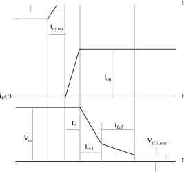 FIGURE 7.7 Trench IGBT structure. VcE(t) FIGURE 7.8 The IGBT turn-on waveforms in a clamped inductive load circuit. During tj-i load current is transferred from the diode into the device and increases to its steady-state value. The gate voltage rise time and IGBT transconductance determine the current slope and as a result t. When the gate-emitter voltage reaches V(3E(ion) that wiU support the steady-state coUector current, coUector-emitter voltage starts to decrease. After this there are two distinct intervals during IGBT turn-on. In the first interval the coUector-to-emitter voltage drops rapidly as the gate-drain capacitance Cgj of the MOSFET portion of IGBT discharges. At low collector-emitter voltage Cgj increases. A finite time is required for high-level injection conditions to set in the drift region. The pnp-transistor portion of IGBT has a slower transition to its on-state than the MOSFET. The gate voltage starts rising again only after the transistor comes out of its saturation region into the linear region, when complete conductivity modulation occurs and the coUector-emitter voltage reaches its final on-state value. 7.4.2 Turn-off Characteristics Turn-off begins by removing the gate-emitter voltage. Voltage and current remain constant until the gate voltage reaches GE(ion) required to maintain the coUector steady-state current as shown in Fig. 7.9. After this delay time (tjof) the coUector voltage rises, whUe the current is held constant. The gate resistance determines the rate of coUector-voltage rise. As the MOS channel turns off, collector current decreases sharply during %i. The MOSFET portion of IGBT determines the turn-off delay time tjff) and the voltage rise time t. When the coUector voltage reaches the bus voltage, the freewheeling diode starts to conduct. However, the excess stored charge in the n~-drift region during on-state conduction must be removed for the device to turn off. The high minority-carrier concentration stored in the n~-drift region supports the collector current after the MOS channel is turned off. Recombination of the minority carriers in the wide-base region gradually decreases the coUector current and results in a current taU. Because there is no access to the base of the pnp-transistor, the excess minority carriers cannot be removed by reverse-biasing the gate. The %2 interval is long because the excess carrier lifetime in this region is normally kept high to reduce the on-state voltage drop. Because the coUector-emitter voltage has reached the bus voltage in this interval a significant power loss occurs that increases with frequency. Therefore, the current taU limits the IGBT operating frequency and there is a trade-off between the on-state losses and faster switching times. For an on-state current of /on the magnitude of current taU, and time required for the coUector current to decrease to 10% of its on-state value, turn-off (tff) time, are approximated as: where T (t) - T (7.4) (7.5) (7.6) GE(t) lC(t) VCE(t) GE(th) CE(on)  FIGURE 7.9 turn-off. Switching waveforms during IGBT clamped inductive load is the gain of the bipolar pnp-transistor, / is the undepleted basewidth and is the ambipolar diffusion length and it is assumed that the high-level lifetime (т^р) is independent of the minority carrier injection during the coUector current decay. Lifetime control techniques are used to reduce the lifetime (thl) and the gain of the bipolar transistor (a). As a resuh the magnitude of the current taU and tff decrease. However, the conductivity modulation decreases, which increases the on-state voltage drop in the drift region. Therefore, higher-speed IGBTs have a lower current rating. Thermal diffusion of impurities such as gold and platinum introduces recombination centers, which reduce the lifetime. The device can also be irradiated with high-energy electrons to generate recombination centers. Electron irradiation introduces a uniform distribution of defects, which results in reduction of lifetime in the entire wafer and affects the conduction properties of the device. Another method of lifetime control is proton implantation, which can place defects at a specific depth. Therefore, it is possible to have a locahzed control of lifetime to improve the trade-off between the on-state voltage and switching speed of the device. The turn-off loss can be minimized by curtaUing the current taU as a result of speeding up the recombination process in the portion of the drift region, which is not swept by the reverse bias. 7.4.3 Latch-up of Parasitic Thyristor A portion of the minority carriers injected into the drift region from the collector of an IGBT flows directly to the emitter terminal. The negative charge of electrons in the inversion layer attracts the majority of holes and generates the lateral component of hole current through the p-type body layer as shown in Fig. 7.10. This lateral current flow develops a voltage drop across the spreading resistance of the p-base region, which forward-biases the base-emitter junction of the npn-parasitic BJT. By designing a small spreading resistance, the voltage drop is lower than the built-in potential and therefore the parasitic thyristor between the p+-collector region, n~-drift region, p-base region, and /7+-emitter does not latch up. Larger values of on-state current density produce a larger voltage drop, which causes injection of electrons from the emitter region into the p-base region and hence turn-on of the /7p/7-transistor. When this occurs the pnp-transistor will turn on, and therefore the parasitic thyristor will latch up and the gate loses control over the collector current. Under dynamic turn-off conditions the magnitude of the lateral hole current flow increases and latch-up can occur at lower on-state currents compared to the static condition. The parasitic thyristor latches up when the sum of the current gains of the npn- and pnp-transistors exceeds one. When the gate voltage is removed from IGBT with a clamped inductive load, its MOSFET component turns off and reduces the MOSFET current to zero very rapidly. As a result the drain-source voltage rises rapidly and is supported by the junction between the n~ -drift region and the p-base region. The drift region has a lower doping and therefore the depletion layer extends more in the drift region. Fience, the current gain of the p/7p-transistor portion, a, increases and a greater portion of FIGURE 7.10 On-state current flow paths in an IGBT structure. the injected holes into the drift region will be collected at the junction of p-base and n~ -drift regions. Therefore, the magnitude of the lateral hole current increases, which increases the lateral voltage drop. As a result the parasitic thyristor will latch up even if the on-state current is less than the static latch-up value. Reducing the gain of the npn- or pnp-transistors can prevent the parasitic thyristor latch-up. A reduction in the gain of the p/7p-transistor increases the IGBT on-state voltage drop. Therefore, in order to prevent the parasitic thyristor latch up it is better to reduce the gain of the npn-transistor component of IGBT. Reduction of carrier lifetime, use of buffer layer, and use of deep p+-diffusion improve the latch-up immunity of IGBT. Fiowever, inadequate extension of the p+-region may fail to prevent the device from latch-up. Also, care should be taken that the p+-diffusion does not extend into the MOS channel because this causes an increase in the MOS threshold voltage. 7.5 IGBT Performance Parameters The IGBTs are characterized by certain performance parameters. The manufacturers specify these parameters, which are described in what follows, in the IGBT data sheet. The important ratings of IGBTs are values that establish either a minimum or maximum limiting capability or limiting condition. The IGBTs cannot be operated beyond the maximum or minimum rating value, which is determined for a specified operating point and environment condition. Collector-Emitter Blocking Voltage (BVqes)- This parameter specifies the maximum off-state collector-emitter voltage when the gate and emitter are shorted. Breakdown is specified at a specific leakage current and varies with temperature by a positive temperature coefficient. Emitter-Collector Blocking Voltage (BVecs)- This parameter specifies the reverse breakdown of the collector-base junction of the pnp-transistor component of IGBT. Gate-Emitter Voltage (Vqes)- This parameter determines the maximum allowable gate-emitter voltage when the collector is shorted to emitter. The thickness and characteristics of the gate-oxide layer determine this voltage. The gate voltage should be limited to a much lower value to limit the collector current under fault conditions. Continuous Collector Current (1): This parameter represents the value of the dc current required to raise the junction to its maximum temperature from a specified case temperature. This rating is specified at a case temperature of 25 °С and maximum junction temperature of 150 °C. Because normal operating condition cause higher case temperatures, a plot is given to show the variation of this rating with case temperature. Peak Collector Repetitive Current (/см)- Under transient conditions the IGBT can withstand higher peak currents compared to its maximum continuous current, which is described by this parameter. Maximum Power Dissipation (P): This parameter represents the power dissipation required to raise the junction temperature to its maximum value of 150 °C, at a case temperature of 25 °C. Normally a plot is provided to show the variation of this rating with temperature. Junction Temperature (Tj): Specifies the aUowable range of the IGBT junction temperature during its operation. Clamped Inductive Load Current (Ilm)- This parameter specifies the maximum repetitive current that IGBT can turn off under a clamped inductive load. During IGBT turn-on, the reverse recovery current of the freewheeling diode in paraUel with the inductive load increases the IGBT turn-on switching loss. Collector-Emitter Leakage Current (Ices)- This parameter determines the leakage current at the rated voltage and specific temperature when the gate is shorted to emitter. Gate-Emitter Threshold Voltage (Удщ): This parameter specifies the gate-emitter voltage range, where the IGBT is turned on to conduct the coUector current. The threshold voltage has a negative temperature coefficient. Threshold voltage increases linearly with gate-oxide thickness and as the square root of the p-base doping concentration. Fixed surface charge at the oxide-sUicon interface and mobUe ions in the oxide shift the threshold voltage. Collector-Emitter Saturation Voltage {Vce(sat))- This parameter specifies the coUector-emitter forward voltage drop and is a function of collector current, gate voltage, and temperature. Reducing the resistance of the MOSFET channel and JFET region, and increasing the gain of the pnp-bipolar transistor can minimize the on-state voltage drop. The voltage drop across the MOSFET component of IGBT, which provides the base current of the pnp-transistor is reduced by a larger channel width, shorter channel length, lower threshold voltage, and wider gate length. Higher minority carrier hfe-time and a thin n-epi region cause high carrier injection and reduce the voltage drop in the drift region. Forward Transconductance (gpE)- Forward transconductance is measured with a smaU variation on the gate voltage, which linearly increases the IGBT coUector current to its rated current at 100 °C. The transconductance of an IGBT is reduced at currents much higher than its thermal-handhng capability. Therefore, unlike the bipolar transistors, the current-handling capabUity of IGBTs is limited by thermal consideration and not by its gain. At higher temperatures, the transconductance starts to decrease at lower collector currents. Therefore these features of transconductance protect the IGBT under short-circuit operation. Total Gate Charge (Qq): This parameter helps to design a suitably sized gate-drive circuit and approximately calculate its losses. Because of the minority-carrier behavior of the device, the switching times cannot be approximately calculated by use of gate-charge value. This parameter varies as a function of the gate-emitter voltage. Turn-on Delay Time (tj): This is defined as the time between 10% of gate voltage to 10% of the final coUector current. Rise Time (t): This is the time required for the coUector current to increase to 90% of its final value from 10% of its final value. Turn-off Delay Time (tioff))- This is the time between 90% of gate voltage to 10% of final collector voltage. Fall Time (tf): This is the time required for the coUector current to drop from 90% of its initial value to 10% of its initial value. Input Capacitance (QJ: The measured gate-emitter capacitance when collector is shorted to emitter. The input capacitance is the sum of the gate-emitter and the MiUer capacitance. The gate-emitter capacitance is much larger than the MiUer capacitance. Output Capacitance (Q): The capacitance between coUector and emitter when the gate is shorted to the emitter, which has the typical pn-junction voltage dependency. Reverse Transfer Capacitance (Q): The Miller capacitance between gate and coUector, which has a complex voltage dependency. Safe Operating Area (SOA): The safe operating area determines the current and voltage boundary within which the IGBT can be operated without destructive faUure. At low currents the maximum IGBT voltage is hmited by the open-base transistor breakdown. The parasitic thyristor latch-up limits the maximum coUector current at low voltages. WhUe IGBTs immune to static latch-up may be vulnerable to dynamic latch-up, operation in short-circuit and inductive load switching are conditions that would subject an IGBT to a combined voltage and current stress. A forward-biased safe operating area (FBSOA) is defined during the turn-on transient of the inductive load switching when both electron and hole current flow in the IGBT in the presence of high voltage across the device. The reverse-biased safe operating area (RBSOA) is defined during the turn-off transient, where only hole current flows in the IGBT with high voltage across it. If the time duration of simultaneous high voltage and high current is long enough, the IGBT faUure wiU occur because of thermal breakdown. However, if this time duration is short, the temperature rise due to power dissipation wiU not be enough to cause thermal breakdown. Under this condition the avalanche breakdown occurs at voltage levels lower than the breakdown voltage of the device. Compared to the steady-state forward blocking condition the much larger charge in the drift region causes a higher electric field and narrower depletion region at the p-base and n~-drift junction. Under RBSOA conditions there is no electron in the space-charge region and therefore there is a larger increase in electric field than the FBSOA condition. 10- s 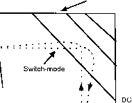 Zero-voltage/ zero current switching 10-4s vbus vbd FIGURE 7.11 The IGBT safe operating area (SOA). The IGBT SOA is indicated in Fig. 7.11. Under short switching times the rectangular SOA shrinks by an increase in the duration of the on-time. Thermal limitation is the reason for smaller SOA and the lower limit is set by dc operating conditions. The device switching loci under hard switching (dashed lines) and zero voltage or zero current switching (solid lines) is also indicated in Fig. 7.11. The excursion is much wider for switch-mode hard-switching apphcations than for the soft-switching case and therefore a much wider SOA is required for hard-switching applications. At present, IGBTs are optimized for hard-switching applications. In soft-switching apphcations the conduction losses of IGBT can be optimized at the cost of smaller SOA. In this case the p-base doping can be adjusted to result in a much lower threshold voltage and hence forward voltage drop. Fiowever, in hard-switching applications the SOA requirements dominate over forward voltage drop and switching time. Therefore, the p-base resistance should be reduced, which causes a higher threshold voltage. As a result, the channel resistance and forward voltage drop will increase. provide the required gate charge for zero current switching and zero voltage switching. The delay of the input signal to the gate drive should be small compared to the IGBT switching period and therefore the gate drive speed should be designed properly to be able to use the advantages of faster switching speeds of the new generation IGBTs. 7.6.1 Conventional Gate Drives The first IGBT gate drives used fixed passive components and were similar to MOSFET gate drives. Conventional gate-drive circuits use a fixed gate resistance for turn-on and turn-off as shown in Fig. 7.12. The turn-on gate resistor R limits the maximum collector current during turn-on, and the turn-off gate resistor iff limits the maximum collector-emitter voltage. In order to decouple the dv/dt and dijdt control an external capacitance can be used at the gate, which increases the time constant of the gate circuit and reduces the diJdt as shown in Fig. 7.13. Fiowever, does not affect the dvJdt transient, which occurs during the Miller plateau region of the gate voltage. 7.6.2 New Gate-Drive Circuits In order to reduce the delay time required for the gate voltage to increase from v~ to V (th), the external gate capacitor can 7.6 Gate-Drive Requirements The gate-drive circuit acts as an interface between the logic signals of the controller and the gate signals of the IGBT, which reproduces the commanded switching function at a higher power level. Nonidealities of the IGBT such as finite voltage and current rise and fall times, turn-on delay, voltage and current overshoots, and parasitic components of the circuit cause differences between the commanded and real waveforms. Gate-drive characteristics affect the IGBT non-idealities. The MOSFET portion of the IGBT drives the base of the p/7p-transistor and therefore the turn-on transient and losses are greatly affected by the gate drive. Due to lower switching losses, soft-switched power converters require gate drives with higher power ratings. The IGBT gate drive must have sufficient peak current capability to FIGURE 7.12 resistors. Gate-drive circuit with independent turn-on and turn-off FIGURE 7.13 External gate capacitor for decoupling dv/dt and di/dt during switching transient. be introduced in the circuit only after V reaches Vg(th) as is shown in Fig. 7.14, where the collector current rise occurs. The voltage tail during turn-on transient is not affected by this method. In order to prevent shoot-through caused by accidental turn-on of IGBT due to noise, a negative gate voltage is required during the off-state. Low gate impedance reduces the effect of noise on the gate. During the first slope of the gate voltage turn-on transient the rate of charge supply to the gate determines the collector-current slope. During the Miller-effect zone of the turn-on transient the rate of charge supply to the gate determines the collector-voltage slope. Therefore, the slope of the coUector current, which is controUed by the gate resistance, strongly affects the turn-on power loss. Reduction in switching power loss requires low gate resistance. However, the coUector-current slope also determines the amplitude of the conducted electromagnetic interference during turn-on switching transient. Lower electromagnetic interference generation requires higher values of gate resistance. Therefore, in conventional gate-drive circuits by selecting an optimum value for R, there is a trade-off between lower switching losses and lower electromagnetic interference generation. However, the turn-off switching of IGBT depends on the bipolar characteristics. Carrier lifetime determines the rate at which the minority carriers stored in the drift region recombine. The charge removed from the gate during turn-off has smaU influence on minority-carrier recombination. The taU current and di/dt during turn-off, which determine the turn-off losses, depend mostly on the amount of stored charge and the minority-carrier lifetime. Therefore, the gate-drive circuit has a minor influence on turn-off losses of the IGBT, whUe it affects the turn-on switching losses. The turn-on transient is improved by use of the circuit shown in Fig. 7.15. The additional current source increases the gate current during the tail voltage time and thus reduces the turn-on loss. The initial gate current is determined by and ion which are chosen to satisfy device electrical specifications and EMI requirements. After the collector current reaches its maximum value, the Miller effect occurs and the controUed-current source is enabled to increase the gate current to increase the rate of coUector-voltage faU. This reduces the turn-on switching loss. Turn-off losses can only be reduced during the Miller effect and MOS turn-off portion of the turn-off transient, by reducing the gate resistance. However, this increases the rate of change of coUector voltage, which strongly affects the IGBT latching current and RBSOA. During the turn-off period, the turn-off gate resistor R determines the maximum rate of coUector-voltage change. After the device turns off, turning on transistor prevents the spurious turn-on of IGBT by preventing the gate voltage from reaching the threshold voltage. 7.6.3 Protection Gate-drive circuits can also provide fault protection of IGBT in the circuit. The fault-protection methods used in IGBT converters are different from their gate-turn-off thyristor (GTO) counterparts. In a GTO converter a crowbar is used for protection and as a result there is no current limiting. When the short-circuit is detected the control circuit turns on aU the GTO switches in the converter, which results in opening of a fuse or circuit breaker on the dc input. Therefore, series di/dt snubbers are required to prevent rapid increase of the fault current and the snubber inductor has to be rated for large currents in the fault condition. However, IGBT has an important abUity to intrinsically limit the current under overcurrent and short-circuit fault conditions, and the value of the fault current can be much larger than the nominal IGBT current. Thus IGBT has to be turned off rapidly after the fault occurs. The magnitude of the fault current depends on the positive-gate bias voltage A higher is required to reduce conduction loss in the device, but this leads to larger fault currents. In order to decouple the trade-off hmitation between conduction loss and fault-current level, a protection circuit can reduce the gate voltage when a fault occurs. However, this does not limit the peak value of the fault current, and therefore a fast fault-detection circuit is required to limit the peak value of the fault current. Fast integrated sensors in the gate-drive circuit are essential for proper IGBT protection. Various methods have been studied to protect IGBTs under fault conditions. One of the techniques uses a capacitor to reduce the gate voltage when the fault occurs. However, FIGURE 7.14 A circuit for reducing the turn-on delay. FIGURE 7.15 Schematic circuit of an IGBT gate-drive circuit. depending on the initial condition of the capacitor and its value, the IGBT current may reduce to zero and then turn on again. Another method is to softly turn off the IGBT after the fault and to reduce the overvoltage due to diJdt. Therefore, the overvoltage on IGBT caused by the parasitic inductance is limited while turning off large currents. The most common method of IGBT protection is collector-voltage monitoring or desaturation detection. The monitored parameter is the collector-emitter voltage, which makes fault detection easier compared to measuring the device current. However, voltage detection can be activated only after the complete turn on of IGBT. If the fault current increases slowly due to large fault inductance, the fault detection is difficult because the collector-emitter voltage will not change significantly. In order to determine whether the current that is being turned off is overcurrent or nominal current, the Miller voltage plateau level can be used. This method can be used to initiate soft turn-off and to reduce the overvoltage during overcurrents. Special sense IGBTs have been introduced at low-power levels with a sense terminal to provide a current signal proportional to the IGBT collector current. A few active device cells are used to mirror the current carried by the other cells. Unfortunately, however, sense IGBTs are not available at high-power levels and there are problems related to the higher conduction losses in the sense device. The most reliable method to detect an overcurrent fault condition is to introduce a current sensor in series with the IGBT. The additional current sensor makes the power circuit more complex and may lead to parasitic bus inductance, which results in higher overvoltages during turn off. After the fault occurs the IGBT has to be safely turned off. Due to large diJdt during turn-off, the overvoltage can be very large. Therefore, many techniques have been investigated to obtain soft turn-off. The most common method is to use a large turn-off gate resistor when the fault occurs. Another method to reduce the turn-off overvoltage is to lower the fault-current level by reducing the gate voltage before initiating the turn-off. A resistive voltage divider can be used to reduce the gate voltage during fault turn-off. For example, the gate-voltage reduction can be obtained by turning on simultaneously ioff and ion the circuit of Fig. 7.12. Another method is to switch a capacitor into the gate and rapidly discharge the gate during the occurrence of a fault. To prevent the capacitor from charging back up to the nominal on-state gate voltage, a large capacitor should be used, which may cause a rapid gate discharge. Also, a Zener diode can be used in the gate to reduce the gate vohage after a fault occurs, but the slow transient behavior of the Zener diode leads to large initial peak fault current. The power dissipation during a fault determines the time duration that the fault current can flow in the IGBT without damaging it. Therefore, the IGBT fault-endurance capability is improved by the use of fault-current limiting circuits to reduce the power dissipation in the IGBT under fault conditions. 7.7 Circuit Models A high-quahty IGBT model for circuit simulation is essential for improving the efficiency and rehability in the design of power electronic circuits. Conventional models for power semiconductor devices simply described an abrupt or linear switching behavior and a fixed resistance during the conduction state. Low switching frequencies of power circuits made it possible to use these approximate models. Fiowever, moving to higher switching frequencies to reduce the size of a power electronic system requires high-quality power semiconductor device models for circuit simulation. The /7-channel IGBT consists of a pnp-bipolar transistor whose base current is provided by an n-channel MOSFET, as is shown in Fig. 7.1. Therefore, the IGBT behavior is determined by physics of the bipolar and MOSFET devices. Several effects dominate the static and dynamic device characteristics. The influence of these effects on a low-power semiconductor device is negligible and therefore they cannot be described by standard device models. The conventional circuit models were developed to describe the behavior of low-power devices, and therefore were not adequate to be modified for IGBT. The reason is that the bipolar transistor and MOSFET in the IGBT have a different behavior compared to their low-power counterparts; they also have different structures. The currently available models have different levels of accuracy at the expense of speed. Circuit issues such as switching losses and reliability are strongly dependent on the device and require accurate device models. Fiowever, simpler models are only adequate for system-oriented issues such as the behavior of an electric motor driven by a pulsewidth modulation (PWM) converter. Finite-element models have high accuracy, but are slow and require internal device structure details. Macromodels are fast but have low accuracy, which depends on the operating point. Commercial circuit simulators have introduced one-dimensional (ID) physics-based models, which offer a compromise between the finite-element models and macromodels. The Fiefner model and the Kraus model are such examples that have been implemented in Saber and there has been some effort to implement them in PSPICE. The Fiefner model depends on the redistribution of charge in the drift region during transients. The Kraus model depends on the extraction of charge from the drift region by the electric field and emitter back-injection. The internal BJT of the IGBT has a wide base, which is lightly doped to support the depletion region to have high blocking voltages. The excess carrier lifetime in the base region is low to have fast turn-off. Fiowever, low-power bipolar transistors have high excess carrier hfetime in the base, narrow base and high current gain. A finite base transit time is required for a change in the injected base charge to change the collector current. Therefore, quasi-static approximation cannot be used at high speeds and the transport of carriers in the base should be described by ambipolar transport theory. 7.7.1 Input and Output Characteristics The bipolar and MOSFET components of a symmetric IGBT are shown in Fig. 7.16. The components between the emitter (e), base (b), and collector (c) terminals correspond to the bipolar transistor and those between gate (g), source (s), and drain (d) are associated with MOSFET. The combination of the drain-source and gate-drain depletion capacitances is identical to the base-coUector depletion capacitance, and therefore they are shown for the MOSFET components. The gate-oxide capacitance of the source overlap (Qs) and source metalhzation capacitance (C) form the gate-source capacitance (C). When the MOSFET is in its linear region the gate-oxide capacitance of the drain overlap (C) forms the gate-drain capacitance (Cj). In the saturation region of MOSFET the equivalent series connection of gate-drain overlap oxide capacitance and the depletion capacitance of the gate-drain overlap (Cgdj) forms the gate-drain Miller capacitance. The gate-drain depletion width and the drain-source depletion width are voltage dependent, which has the same effect on the corresponding capacitances. The most important capacitance in IGBT is the capacitance between the input terminal (g) and output terminal (a), because the switching characteristics are affected by this feedback. a. =42 = с * dv,. (7.7) is determined by the oxide thickness and device area. The accumulation, depletion, and inversion states below the gate Cathode 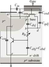 cause different states of charge and therefore different capacitance values. The stored charge in the lightly doped wide base of the bipolar component of IGBT causes switching delays and switching losses. The standard quasi-static charge description is not adequate for IGBT because it assumes that the charge distribution is a function of the IGBT terminal voltage. However, the stored charge density {p{x,t)) changes with time and position and therefore the ambipolar diffusion equation must be used to describe the charge variation: dP(x, t) dt P(x, t) dPjx, t) T. dx (7.8) Anode FIGURE 7.16 Symmetric IGBT half cell. The slope of the charge-carrier distribution determines the sum of electron and hole currents. The nonquasistatic behavior of the stored charge in the base of the bipolar component of IGBT results in the collector-emitter redistribution capacitance (Q.). This capacitance dominates the output capacitance of IGBT during turn-off and describes the rate of change of the base-coUector depletion layer with the rate of change of the base-coUector voltage. However, the base-coUector displacement current is determined by the gate-drain (Cjj) and drain-source (Q) capacitance of the MOSFET component. 7.7.2 Implementing the IGBT Model into a Circuit Simulator Usually a netlist is employed in a circuit simulator such as Saber to describe an electrical circuit. Each component of the circuit is defined by a model template with the component terminal connection and the model parameters values. WhUe Saber libraries provide some standard component models, the models can be generated by implementing the model equations in a defined Saber template. Electrical component models of IGBT are defined by the current through each component element as a function of component variables, such as terminal and internal node voltages and explicitly defined variables. The circuit simulator uses the Kirchhoff current law to solve for electrical component variables such that the total current into each node is equal to zero, whUe satisfying the exphcitly defined component variables needed to describe the state of the device. The IGBT circuit model is generated by defining the currents between terminal nodes as a nonlinear function of component variables and their rate of change. An IGBT circuit model is shown in Fig. 7.17. Compared to Fig. 7.16 the bipolar transistor is replaced by the two base and coUector-current sources. There is a distributed voltage drop due to diffusion and drift in the base regions. The drift terms in the ambipolar diffusion equation depend on base and collector currents. Therefore, both of these currents generate the resistive voltage drop and i is placed at the emitter terminal in the IGBT circuit model. The capacitance of the emitter-base junction 1 ... 8 9 10 11 12 13 14 ... 91 |
|
© 2026 AutoElektrix.ru
Частичное копирование материалов разрешено при условии активной ссылки |