 |
 |
 |
| Главная Журналы Популярное Audi - почему их так назвали? Как появилась марка Bmw? Откуда появился Lexus? Достижения и устремления Mercedes-Benz Первые модели Chevrolet Электромобиль Nissan Leaf |
Главная » Журналы » Metal oxide semiconductor 1 ... 9 10 11 12 13 14 15 ... 91 (Q) is implicitly defined by the emitter-base voltage as a function of base charge; Iy is the emitter-base capacitor current that defines the rate of change of the base charge. The current through the collector-emitter redistribution capacitance is part of the collector current, which in contrast to depends on the rate of change of the base-emitter voltage; is part of the base current that does not flow through and does not depend on the rate of change of base-collector voltage. Impact ionization causes carrier multiphcation in the high electric field of the base-collector depletion region. This carrier multiphcation generates an additional base-collector current component (4iuit) which is proportional to 4, 1, and the multiplication factor. The resulting Saber IGBT model should be able to describe accurately the experimental results for the range of static and dynamic conditions where IGBT operates. Therefore, the model can be used to describe the steady-state and dynamic characteristics under various circuit conditions. The currently available models have different levels of accuracy at the expense of speed. Circuit issues such as switching losses and rehability are strongly dependent on the device and require accurate device models. However, simpler models are adequate for system-oriented issues such as the behavior of an electric motor driven by a PWM converter. Finite-element models have high accuracy, but are slow and require internal device structure details. Macromodels are fast but have low accuracy, which depends on the operating point. Commercial circuit simulators have introduced ID physics-based models, which offer a compromise between the finite-element models and macromodels. cathode 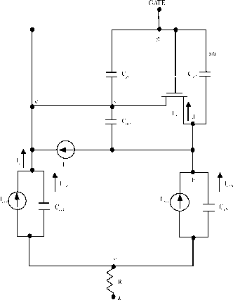 anode FIGURE 7.17 IGBT circuit model. 7.8 Applications Power electronics evolution is a result of the evolution of power semiconductor devices. Applications of power electronics are still expanding in industrial and utility systems. A major challenge in designing power electronic systems is simultaneous operation at high power and high switching frequency. The advent of IGBTs has revolutionized power electronics by extending the power and frequency boundary. During the last decade the conduction and switching losses of IGBTs have been reduced in the process of transition from the first- to the third-generation IGBTs. The improved characteristics of the IGBTs have resulted in higher switching speed and lower energy losses. High-voltage IGBTs are expected to take the place of high-voltage GTO thyristor converters in the near future. To advance the performance beyond the third-generation IGBTs, the fourth-generation devices will require exploiting fine-line lithographic technology and employing the trench technology used to produce power MOSFETs with very low on-state resistance. Intelhgent IGBT or intelligent power module (IPM) is an attractive power device integrated with circuits to protect against overcurrent, overvoltage, and overheating. The main application of IGBT is for use as a switching component in inverter circuits, which are used in both power supply and motor drive applications. The advantages of using IGBT in these converters are simplicity and modularity of the converter, simple gate drive, elimination of snubber circuits due to the square SOA, lower switching loss, improved protection characteristics in case of overcurrent and short-circuit fault, galvanic isolation of the modules, and simpler mechanical construction of the power converter. These advantages have made the IGBT the preferred switching device in the power range below 1 MW. Power supply applications of IGBTs include uninterruptible power supplies (UPS) as is shown in Fig. 7.18, constant-voltage constant-frequency power supplies, induction heating systems, switch mode power supplies, welders (Fig. 7.19), cutters, traction power supplies, and medical equipment (CT, X-ray). Low-noise operation, small size, low cost and high accuracy are characteristics of the IGBT converters in these applications. Examples of motor drive applications include the variable-voltage variable-frequency inverter as is shown in Fig. 7.20. The IGBTS have been introduced at high voltage and current levels, which has enabled their use in high-power converters utilized for medium-voltage motor drives. The improved characteristics of the IGBTs have introduced power converters in megawatt power apphcations such as traction drives. One of the critical issues in realizing high-power converters is the rehability of the power switches. The devices used in these applications must be robust and capable of withstanding faults long enough for a protection scheme to be activated. The hard-switching voltage source power converter is the most commonly used topology. In this switch-mode operation the switches are subjected to high switching stresses and high-switching power loss that increase hnearly with the switching frequency of the pulsewidth modulation (PWM). The resulting switching loci in the - ц plane is shown by the dotted lines in Fig. 7.11. Because of simultaneous large switch voltage and large switch current, the switch must be capable of withstanding high switching stresses with a large SOA. The requirement of being able to withstand large stresses results in design compromises in other characteristics of the power semiconductor device. Often forward voltage drop and switching speed are sacrificed for enhanced short-circuit capability. Process parameters of the IGBT such as threshold voltage, carrier hfetime, and the device thickness can be varied to obtain various combinations of SOA, on-state voltage, and switching time. However, there is very little overlap in the optimum combination for more than one performance parameter. Therefore, improved performance in one parameter is achieved at the cost of other parameters. In order to reduce the size, the weight, and the cost of circuit components used in a power electronics converter very high switching frequencies of the order of a few megahertz are being contemplated. In order to be able to increase the switching frequency, the problems of switch stresses, switching losses and the EMI associated with switch-mode applications need to be solved. Use of soft-switching converters reduces the problems of high dv/dt and high di/dt by use of external inductive and capacitive components to shape the switching trajectory of the device. The device-switching loci resulting from soft switching is shown in Fig. 7.11, where significant reduction in switching stress can be noticed. The traditional FIGURE 7.19 IGBT welder. snubber circuits achieve this goal without the added control complexity, but the power dissipation in these snubber circuits can be large and limit the switching frequency of the converter. Also, passive components significantly add to the size, weight, and cost of the converter at high power levels. Soft switching uses lossless resonant circuits, which solves the problem of power loss in the snubber circuit, but increases the conduction loss. Resonant transition circuits eliminate the problem of high peak device stress in the soft-switched converters. The main drawback of these circuits is the increased control complexity required to obtain the resonant switching transition. The large number of circuit variables to be sensed in such power converters can affect their reliability. With short-circuit capability no longer being the primary concern, designers can push the performance envelope for their circuits until the device becomes the limiting factor once again. The transient response of the conventional volts/hertz induction motor drive is sluggish because both torque and flux are functions of stator voltage and frequency. Use of vector or field-oriented control methods makes the performance of the induction motor drive almost identical to that of a separately excited dc motor. Therefore, the transient response is similar to a dc machine, where torque and flux can be controlled in a decoupled manner. Vector-controUed induction motors with shaft encoders or speed sensors have been widely apphed in combination with voltage-source PWM inverters using IGBT modules. According to the specification of the new products, vector-controUed induction motor drive systems ranging from kilowatts to megawatts provide a broad range of speed control, constant torque operation, and high starting torque. FIGURE 7.18 Constant-voltage, constant-frequency inverter (UPS). FIGURE 7.20 Variable-voltage, variable-frequency inverter (PWM). Because of their simple gate drives and modular packaging, IGBTs led to simpler construction of power electronic circuits. This feature has lead to a trend to standardize and modularize power electronic circuits. Simplification of the overall system design and construction and significant cost reduction are the main imphcations of this approach. With these goals the Power Electronics Building Block (PEBB) program has been introduced, where the entire power electronic converter system is reduced to a single block. Similar modular power electronic blocks are commercially available at low power levels in the form of power-integrated circuits. At higher power levels, these blocks have been realized in the form of intelligent power modules and power blocks. However, these high-power modules do not encompass entire power electronic systems such as motor drives and UPS. The aim of the PEBB program is to realize the whole power-handling system within standardized blocks. A PEBB is a universal power processor that changes any electrical power input to any desired form of voltage, current and frequency output. A PEBB is a single package with a multifunction controller that replaces the complex power electronic circuits with a single device and therefore reduces the development and design costs of the complex power circuits and simphfies the development and design of large electric power systems. The apphcations of power electronics are varied and various apphcations have their own specific design requirement. There is a wide choice of available power devices. Because of physical, material and design limitations none of the currently available devices behave as an ideal switch, which should block arbitrarily large forward and reverse voltages with zero current in the off-state, conduct arbitrarily large currents with zero-voltage drop in the on-state, and have negligible switching time and power loss. Therefore, power electronic circuits should be designed by considering the capabilities and limitations of available devices. Traditionally, there has been limited interaction between device manufacturers and circuit designers. Thus manufacturers have been fabricating generic power semiconductor devices with inadequate consideration of the specific applications where the devices are used. The diverse nature of power electronics does not allow the use of generic power semiconductor devices in all applications as it leads to nonoptimal systems. Therefore, the devices and circuits need to be optimized at the application level. Soft switching topologies offer numerous advantages over conventional hard-switching applications such as reduced switching stress and EMI, and higher switching speed at reduced power loss. The IGBTs behave dissimilarly in the two circuit conditions. As a result devices optimized for hard-switching conditions do not necessarily give the best possible performance when used in soft-switching circuits. In order to extract maximum system performance, it is necessary to develop IGBTs suited for specific apphcations. These optimized devices need to be manufacturable and cost effective in order to be commercially viable. References 1. Adler, M. S., Owyang, K. W., Baliga, B. J., and Kokosa, R. A., The evolution of power device technology IEEE Trans. Electron. Devices ED-31: 1570-1591 (1984). 2. Akagi, H., The state-of-the-art of power electronics in Japan, IEEE Trans. Power Electron. 13: 345-356 (1998). 3. Baliga, B. J., Adler, M. S., Love, R. R, Gray, R V., and Zommer, N., The insulated gate transistor: a new three-terminal MOS controlled bipolar power device, IEEE Trans. Electron. Devices ED-31: 821-828 (1984). 4. Baliga B. J., Power Semiconductor Devices, PWS Publishing, Boston, 1996. 5. Blaabjerg, R and Pedersen, J. K., An optimum drive and clamp circuit design with controlled switching for a snubberless PWM-VSI-IGBT inverterleg, in IEEE Power Electronics Specialists Conference Records, pp. 289-297, 1992. 6. Chokhawala, R. and Castino, G., IGBT fault current limiting circuits, in IEEE Industry Applications Society Annual Meeting Records, pp. 1339-1345, 1993. 7. Clemente, S. et al., IGBT Characteristics, IR Applications Note AN-983A. 8. Divan, D. M. and Skibinski, G., Zero-switching-loss inverters for high power applications, IEEE Trans. Industry Applications 25: 634-643 (1989). 9. Elasser, A., Parthasarathy, V., and Torrey, D., A study of the internal device dynamics of punch-through and non punch-through IGBTs under zero-current switching, IEEE Trans. Power Electron. 12: 21-35 (1997). 10. Ghandi, S. K., Semiconductor Power Devices, John Wiley & Sons, NY, 1977. 11. Hefner, A. R., An improved understanding for the transient operation of the insulated gate bipolar transistor (IGBT), IEEE Trans. Power Electron. 5: 459-468 (1990). 12. Hefner, A. R. and Blackburn, D. L., An analytical model for the steady-state and transient characteristics of the power insulated gate bipolar transistor, Solid-State Electron. 31: 1513-1532 (1988). 13. Hefner, A. R., An investigation of the drive circuit requirements for the power insulated gate bipolar transistor (IGBT), IEEE Trans. Power Electron. 6: 208-219 (1991). 14. Jahns, T.M. Designing intelligent muscle into industrial motion control, in Industrial Electronics Conference Records, 1-14, 1989. 15. John, v., Suh, B. S., and Lipo, T. A., Fast clamped short circuit protection of IGBTs, in IEEE Applied Power Electronics Conference Records, pp. 724-730, 1998. 16. Kassakian, J. G., Schlecht, M. R, and Verghese, G. C., Principles of Power Electronics, Addison Wesley, 1991. 17. Kraus, R. and Hoffman, K., An analytical model of IGBTs with low emitter efficiency, in ISPSD93, pp. 30-34. 18. Lee, H. G., Lee, Y. H., Suh, B. S., and Lee, J. W, A new intelligent gate control scheme to drive and protect high power IGBTs, in European Power Electronics Conference Records, pp. 1.400-1.405, 1997. 19. Licitra, C., Musumeci, S., Raciti, A., Galluzzo, A. U., and Letor, R., A new driving circuit for IGBT devices, IEEE Trans. Power Electron. 10: 373-378 (1995). 20. McMurray, W., Resonant snubbers with auxiliary switches, IEEE Trans. Industry Applications 29: 355-362 (1993). 21. Mohan, N., Undeland, T, and Robbins, W, Power Electronics - Design, Converters and Applications, John Wiley & Sons, NY, 1996. 22. Penharkar, S., and Shenai, K., Zero voltage switching behavior of punchthrough and nonpunchthrough insulated gate bipolar transistors (IGBTs), IEEE Trans. Electron. Devices 45: 1826-1835 (1998). 23. Powerex IGBTMOD and intellimod-Intelligent Power Modules Applications and Technical Data Book, 1994. 24. Sze, S. M., Physics of Semiconductor Devices, John Wiley & Sons, NY, 1981. 25. Sze, S. M., Modern Semiconductor Device Physics, John Wiley & Sons, NY, 1998. 26. Trivedi, M., Pendharkar, S., and Shenai, K., Switching characteristics of IGBTs and MCTs in power converters, IEEE Trans. Electron. Devices 43: 1994-2003 (1996). 27. Trivedi, M. and Shenai, K., Modeling the turn-off of IGBTs in hard-and soft-switching applications, IEEE Trans. Electron. Devices 44: 887-893 (1997). 28. Trivedi, M. and Shenai, K., Internal dynamics of IGBT under zero- voltage and zero-current switching conditions, IEEE Trans. Electron. Devices 46: 1274-1282 (1999). 29. Trivedi, M. and Shenai, K., Failure mechanisms of IGBTs under short-circuit and clamped inductive switching stress, IEEE Trans. Power Electron. 14: 108-116 (1999). 30. Undeland, Т., Jenset, R, Steinbakk, A., Ronge, Т., and Hemes M., A snubber configuration for both power transistor and GTO PWM inverters, in IEEE Power Electronics Specialists Conference Records, pp. 42-53, 1984. 31. Venkatesan, V., Eshaghi, M., Borras, R., and Deuty, S., IGBT turn-off characteristics explained through measurements and device simulation, in IEEE Applied Power Electronics Conference Records, pp. 175-178, 1997. 32. Widjaja, I., Kurnia, A., Shenai, K., and Divan, D., Switching dynamics of IGBTs in soft-switching converters, IEEE Trans. Electron. Devices, 42: 445-454 (1995). MOS Controlled Thyristors (MCTs) S. Yuvarajan, Ph.D. Department of Electrical Engineering, North Dakota State University, P.O. Box 5285, Fargo, North Dakota 58105-5285, USA 1.1 Introduction...................................................................................... 117 1.2 Equivalent Circuit and Switching Characteristics..................................... 118 8.2.1 Turn-on and Turn-off 1.3 Comparison of MCT and Other Power Devices....................................... 119 1.4 Gate Drive for MCTs.......................................................................... 119 1.5 Protection of MCTs............................................................................ 120 8.5.1 Paralleling of MCTs 8.5.2 Overcurrent Protection 1.6 Simulation Model of an MCT.............................................................. 120 1.7 Generation-1 and Generation-2 MCTs................................................... 121 1.8 N-channelMCT................................................................................. 121 1.9 Base Resistance-Controlled Thyristor..................................................... 121 1.10 MOS Turn-Off Thyristor..................................................................... 121 1.11 Applications of PMCT......................................................................... 122 8.11.1 Soft-switching 8.11.2 Resonant Converters 1.12 Conclusions....................................................................................... 123 1.13 Appendix.......................................................................................... 123 8.13.1 Description References......................................................................................... 124 8.1 Introduction The efficiency, capacity, and ease of control of power converters depend mainly on the power devices employed. Power devices, in general, belong to either bipolar-junction type or field-effect type and each one has its advantages and disadvantages. The silicon controlled rectifier (SCR), also known as a thyristor, is a popular power device that has been used over the past several years. It has a high current density and a low forward voltage drop, both of which make it suitable for use in large power applications. The inability to turn off through the gate and the low switching speed are the main limitations of an SCR. The gate turn-off (GTO) thyristor was proposed as an ahernative to SCR. However, the need for a higher gate turn-off current limited its apphcation. The power MOSFET has several advantages such as high input impedance, ease of control, and higher switching speeds. Lower current density and higher forward drop limited the device to low-voltage and low-power applications. An effort to combine the advantages of bipolar junction and field-effect structures has resulted in hybrid devices such as the insulated gate bipolar Transistor (IGBT) and the MOS controlled thyristor (MCT). While an IGBT is an improvement over a bipolar junction transistor (BJT) using a MOSFET to turn on and turn off current, an MCT is an improvement over a thyristor with a pair of MOSFETs to turn on and turn off current. The MCT overcomes several of the limitations of the existing power devices and promises to be a better switch for the future. While there are several devices in the MCT family with distinct combinations of channel and gate structures [1], one type, called the P-channel MCT, has been widely reported and is discussed here. Because the gate of the device is referred to with respect to the anode rather than the cathode, it is sometimes referred to as a complementary MCT (C-MCT) [2]. Harris Semiconductors (Intersil) originally made the MCTs, but the MCT division was sold to Silicon Power Corporation (SPCO), which has continued the development of MCTs. 8.2 Equivalent Circuit and Switching Characteristics The SCR is a 4-layer pnpn device with a control gate, and applying a positive gate pulse turns it on when it is forward-biased. The regenerative action in the device helps to speed up the turn-on process and to keep it in the ON state even after the gate pulse is removed. The MCT uses an auxiliary MOS device (PMOSFET) to turn on and this simplifies the gate control. The turn-on has aU the characteristics of a power MOSFET. The turn-off is accomplished using another Anode - 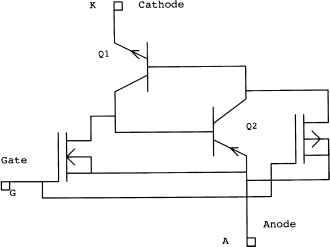  Metal Oxide I I I I I J I I I I I I I Il I I I Metal Oxide IIIIIIIIIII I I I Il I I I I --У n (pnp base, Off-FET drain) p- (npn base, On-FET drain) p buffer, epitaxial layer n+ substrate Gate FIGURE 8.1 Equivalent circuit and symbol of an MCT. - Cathode FIGURE 8.2 Cross section of an MCT unit cell. MOSFET (NMOSFET), which essentially diverts the base current of one of the BJTs and breaks the regeneration. The transistor-level equivalent circuit of a P-channel MCT and the circuit symbol are shown in Fig. 8.1. The cross section of a unit ceU is shown in Fig. 8.2. The MCT is modeled as an SCR merged with a pair of MOSFETs. The SCR consists of the bipolar junction transistors (BJTs) and Q2, which are interconnected to provide regenerative feedback such that the transistors drive each other into saturation. Of the two MOSFETs, the PMOS located between the coUector and emitter of Q2 helps to turn the SCR on, and the NMOS located across the base-emitter junction of Q2 turns it off. In the actual fabrication, each MCT is made up of a large number (~ 100,000) cells, each of which contains a wide-base npn transistor and a narrow-base pnp transistor. While each pnp transistor in a ceU is provided with an N-channel MOSFET across its emitter and base, only a smaU percentage (~4%) of pnp transistors are provided with P-channel MOSFETs across their emitters and coUectors. The smaU percentage of PMOS cells in an MCT provides just enough current for turn-on and the large number of NMOS cells provide plenty of current for turn-off. 8 MOS Controlled Thyristors (MCTs) 8.2.1 Turn-on and Turn-off When the MCT is in the forward blocking state, it can be turned on by applying a negative pulse to its gate with respect to the anode. The negative pulse turns on the PMOSFET (On-FET) whose drain current flows through the base-emitter junction of Ql (npn) thereby turning it on. The regenerative action within - Q2 turns the MCT on into full conduction within a very short time and maintains it even after the gate pulse is removed. The MCT turns on without a plasma-spreading phase giving a high dl/dt capability and ease of overcurrent protection. The on-state resistance of an MCT is slightly higher than that of an equivalent thyristor because of the degradation of the injection efficiency of the iV+ emitter/p-base junction. Also, the peak current rating of an MCT is much higher than its average or rms current rating. An MCT will remain in the ON state until the device current is reversed or a turn-off pulse is applied to its gate. Applying a positive pulse to its gate turns off a conducting MCT. The positive pulse turns on the NMOSFET (Off-FET), thereby diverting the base current of Q2 (pnp) away to the anode of the MCT and breaking the latching action of the SCR. This stops the regenerative feedback within the SCR and turns the MCT off. All the cells within the device are to be turned off at the same time to avoid a sudden increase in current density. When the Off-FETs are turned on, the SCR section is heavily shorted and this results in a high dV/dt rating for the MCT. The highest current that can be turned off with the application of a gate bias is called the maximum controllable current. The MCT can be gate controlled if the device current is less than the maximum controllable current. For smaller device currents, the width of the turn-off pulse is not critical. Fiowever, for larger currents, the gate pulse has to be wider and more often has to occupy the entire off-period of the switch. 8.3 Comparison of MCT and Other Power Devices An MCT can be compared to a power MOSFET, a power BJT, and an IGBT of similar voltage and current ratings. The operation of the devices is compared under on-state, off-state, and transient conditions. The comparison is simple and very comprehensive. The current density of an MCT is 70% higher than that of an IGBT having the same total current [2]. During its on-state, an MCT has a lower conduction drop compared to other devices. This is attributed to the reduced cell size and the absence of emitter shorts present in the SCR within the MCT. The MCT also has a modest negative temperature coefficient at 1000 w 100 (U tr H>. 10
0.0 0.5 1.0 1.5 2.0 2.5 Conduction drop (volts) FIGURE 8.3 Comparison of forward drop for different devices. lower currents with the temperature coefficient turning positive at larger current [2]. Figure 8.3 shows the conduction drop as a function of current density. The forward drop of a 50-A MCT at 25 °С is around 1.1 V, while that for a comparable IGBT is over 2.5 V. The equivalent voltage drop calculated from the value of r2)5(ON) for a power MOSFET will be much higher. Fiowever, the power MOSFET has a much lower delay time (30 ns) compared to that of an MCT (300 ns). The turn-on of a power MOSFET can be so much faster than an MCT or an IGBT therefore, the switching losses would be negligible compared to the conduction losses. The turn-on of an IGBT is intentionally slowed down to control the reverse recovery of the freewheeling diode used in inductive switching circuits [3]. The MCT can be manufactured for a wide range of blocking voltages. Turn-off speeds of MCTs are supposed to be higher as initially predicted. The turn-on performance of Generation-2 MCTs are reported to be better compared to Generation-1 devices. Even though the Generation-1 MCTs have higher turn-off times compared to IGBTs, the newer ones with higher radiation (hardening) dosage have comparable turn-off times. At present, extensive development activity in IGBTs has resulted in high-speed switched mode power supply (SMPS) IGBTs that can operate at switching speeds 150kFiz [4]. The turn-off delay time and the fall time for an MCT are much higher compared to a power MOSFET, and they are found to increase with temperature [2]. Power MOSFETs becomes attractive at switching frequencies above 200 kFiz, and they have the lowest turn-off losses among the three devices. The turn-off safe operating area (SOA) is better in the case of an IGBT than an MCT. For an MCT, the full switching current is sustainable at 50 to 60% of the breakdown voltage rating, while for an IGBT it is about 80%. The use of capacitive snubbers becomes necessary to shape the turn-off locus of an MCT. The addition of even a smaU capacitor improves the SOA considerably. 8.4 Gate Drive for MCTs The MCT has a MOS gate similar to a power MOSFET or an IGBT and hence it is easy to control. In a PMCT, the gate voltage must be applied with respect to its anode. A negative voltage below the threshold of the On-FET must be applied to turn on the MCT. The gate voltage should faU within the specified steady-state limits in order to give a reasonably low delay time and to avoid any gate damage due to overvoltage [3]. Similar to a GTO, the gate voltage rise-time has to be limited to avoid hot spots (current crowding) in the MCT ceUs. A gate voltage less than -5V for turn-off and greater than 10 V for turn-on ensures proper operation of the MCT. The latching of the MCT requires that the gate voltage be held at a positive level in order to keep the MCT turned off. Because the peak-to-peak voltage levels required for driving the MCT exceeds those of other gate-controlled devices, the use of commercial drivers is hmited. The MCT can be turned on and off using a push-puU pair with discrete NMOS-PMOS devices, which, in turn, are driven by commercial integrated circuits (ICs). However, some drivers developed by MCT manufacturers are not commercially available [3]. A Bakers clamp push-puU can also be used to generate gate pulses of negative and positive polarity of adjustable width for driving the MCT [5-7]. The Bakers clamp ensures that the push-pull transistors wiU be in the quasi-saturated state prior to turn-off and this results in a fast switching action. Also, the negative feedback built into the circuit ensures satisfactory operation against variations in load and temperature. A similar circuit with a push-puU transistor pair in parallel with a pair of power BJTs is available [8]. An intermediate section, with a BJT that is either cut off or saturated, provides - 10 and +15 V through potential division. 8.5 Protecrion of MCTs 8.5.1 Paralleling of MCTs Similar to power MOSFETs, MCTs can be operated in parallel. Several MCTs can be paraUeled to form larger modules with only slight derating of the individual devices provided the devices are matched for proper current sharing. In particular, the forward voltage drops of individual devices have to be matched closely. 8.5.2 Overcurrent Protection The anode-to-cathode voltage in an MCT increases with its anode current and this property can be used to develop a protection scheme against overcurrent [5, 6]. The gate pulses to the MCT are blocked when the anode current and hence the anode-to-cathode voltage exceeds a preset value. A Schmitt trigger comparator is used to allow gate pulses to the MCT when it is in the process of turning on, during which time the anode voltage is relatively large and decreasing. 8.5.2.1 Snubbers As with any other power device, the MCT is to be protected against switching-induced transient voltage and current spikes by using suitable snubbers. The snubbers modify the voltage and current transients during switching such that the switching trajectory is confined within the safe operating area (SOA). When the MCT is operated at high frequencies, the snubber increases the switching loss due to the delayed voltage and current responses. The power circuit of an MCT chopper including an improved snubber circuit is shown in Fig. 8.4 [5, 7]. The turn-on snubber consists of and Dg and the turn-off snubber consists of R, Q, and Dq. The series-connected turn-on snubber reduces the rate of change of the anode current dij/dt. The MCT does not support until the current through the freewheeling diode reaches zero at turn-on. The turn-off snubber helps to reduce the peak power and the total power dissipated by the MCT by reducing the voltage across the MCT when the anode current decays to zero. The analysis and design of the snubber and the effect of the snubber on switching loss and electromagnetic interference are given in References [5] and [7]. An alternative snubber configuration for the two MCTs in an ac-ac converter has also been reported [8]. This snubber uses only one capacitor and one inductor for both the MCT switches (PMCT and NMCT) in a power-converter leg. Kb R-L Load Gate FIGURE 8.4 An MCT chopper with turn-on and turn-off snubbers. 8.6 Simulation Model of an MCT The operation of power converters can be analyzed using PSPICE and other simulation software. As it is a new device, models of MCTs are not provided as part of the simulation libraries. However, an appropriate model for the MCT would be helpful in predicting the performance of novel converter topologies and in designing the control and protection circuits. Such a model must be simple enough to keep the simulation time and effort at a minimum, and must represent most of the device properties that affect the circuit operation. The PSPICE models for Harris PMCTs are provided by the manufacturer and can be downloaded from the internet. However, a simple model presenting most of the characteristics of an MCT is available [9, 10]. It is derived from the transistor-level equivalent circuit of the MCT by expanding the SCR model already reported the literature. The improved model [10] is capable of simulating the breakover and breakdown characteristics of an MCT and can be used for the simulation of high-frequency converters. 8.7 Generation-1 and Generation-2 MCTs The Generation-1 MCTs were commercially introduced by Harris Semiconductors in 1992. However, the development of Generation-2 MCTs is continuing. In Gen-2 MCTs, each cell has its own turn-on field-effect transistor (FET). Preliminary test results on Generation-2 devices and a comparison of their performance with those of Generation-1 devices and highspeed IGBTs are available [11, 12]. The Generation-2 MCTs have a lower forward drop compared to the Generation-1 MCTs. They also have a higher dl/dt rating for a given value of capacitor used for discharge. During hard switching, the fall time and the switching losses are lower for the Gen-2 MCTs. The Gen-2 MCTs have the same conduction loss characteristics as Gen-1 with drastic reductions in turn-off switching times and losses [13]. Under zero-current switching conditions, Gen-2 MCTs have negligible switching losses [13]. Under zero-voltage switching, the turn-off losses in a Gen-2 device are one-half to one-fourth (depending on temperature and current level) the turn-off losses in Gen-1 devices. In all soft-switching applications, the predominant loss, namely, the conduction loss, reduces drastically allowing the use of fewer switches in a module. 8.8 N-channel MCT The PMCT discussed in this chapter uses an NMOSFET for turn-off and this results in a higher turn-off current capability. The PMCT can only replace a P-channel IGBT and inherits all the limitations of a P-channel IGBT. The results of a 2D simulation show that the NMCT can have a higher controllable current [13]. It is reported that NMCT versions of almost all Harris PMCTs have been fabricated for analyzing the potential for a commercial product [3]. The NMCTs are also being evaluated for use in zero-current soft-switching applications. However, the initial results are not quite encouraging in that the peak turn-off current of an NMCT is one-half to one-third of the value achievable in a PMCT. It is hoped that the NMCTs will eventually have a lower switching loss and a larger SOA as compared to PMCTs and IGBTs. 8.9 Base Resistance-Controlled Thyristor [14] The base resistance-controlled thyristor (BRT) is another gate-controlled device that is similar to the MCT but with a different structure. The Off-FET is not integrated within the p-base region but is formed within the n-base region. The diverter region is a shallow p-type junction formed adjacent to the p-base region of the thyristor. The fabrication process is simpler for this type of structure. The transistor level equivalent circuit of a BRT is shown in Fig. 8.5. The BRT will be in the forward blocking state with a positive voltage applied to the anode and with a zero gate bias. The forward blocking voltage will be equal to the breakdown voltage of the open-base pnp transistor. A positive gate bias turns on the BRT. At low current levels, the device behaves similarly to an IGBT. When the anode current increases, the operation changes to thyristor mode resulting in a low forward FIGURE 8.5 (BRT). Equivalent circuit of base resistance-controlled thyristor drop. Applying a negative voltage to its gate turns off the BRT. During the turn-off process, the anode current is diverted from the iV+ emitter to the diverter. The BRT has a current tail during turn-off that is similar to an MCT or an IGBT. MCT, turns off the MTOT. The voltage pulse turns on the FET, thereby shorting the emitter and base of the npn transistor and breaking the regenerative action. The MTOT is a faster switch than a GTO in that it is turned off with a reduced storage time compared to a GTO. The disk-type construction aUows double-side cooling. 8.10 MOS Turn-off Thyristor [15] The MOS turn-off (MTO) thyristor or the MTOT is a replacement for the GTO and it requires a much smaUer gate drive. It is more efficient than a GTO, it can have a maximum blocking voltage of about 9 kV, and it wiU be used to buUd power converters in the 1- to 20-MVA range. SUicon Power Corporation (SPCO) manufactures the device. The transistor-level equivalent circuit of the MTOT (hybrid design) and the circuit symbol are shown in Fig. 8.6. Applying a current pulse at the turn-on gate (Gl), as with a conventional GTO, turns on the MTOT. The turn-on action, including regeneration, is simUar to a conventional SCR. Applying a positive voltage pulse to the turn-off gate (G2), as with an 8.11 Applications of PMCT The MCTs have been used in various applications, some of which are in the area of ac-dc and ac-ac conversion where the input is 60-Hz ac. Variable power factor operation was achieved using the MCTs as a force-commutated power switch [5]. The power circuit of an ac voltage controUer capable of operating at a leading, lagging, and unity power factor is shown in Fig. 8.7. Because the switching frequency is low, the switching losses are negligible. Because the forward drop is low, the conduction losses are also smaU. The MCTs are also used in circuit breakers. к Cathode Turn-on Gate Gl ~ Turn-off Gate A Anode 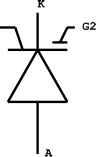 FIGURE 8.6 Equivalent circuit and symbol of a MOS turn-off (MTO) thyristor. 8.11.1 Soft-switching The MCT is intended for high-frequency switching apphcations where it is supposed to replace a MOSFET or an IGBT. SimUar to a Power MOSFET or an IGBT, the switching losses wiU be high at high switching frequencies. The typical characteristics of an MCT during turn-on and turn-off under hard switching (without snubber) are shown in Fig. 8.8. During turn-on and turn off, the device current and voltage take a finite time to reach their steady-state values. Each time the device changes state, there is a short period during which the voltage and current variations overlap. This results in a transient power loss that contributes to the average power loss.
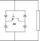 FIGURE 8.7 Power circuit of MCT ac voltage controller. 1 ... 9 10 11 12 13 14 15 ... 91 |
|
© 2026 AutoElektrix.ru
Частичное копирование материалов разрешено при условии активной ссылки |