 |
 |
 |
| Главная Журналы Популярное Audi - почему их так назвали? Как появилась марка Bmw? Откуда появился Lexus? Достижения и устремления Mercedes-Benz Первые модели Chevrolet Электромобиль Nissan Leaf |
Главная » Журналы » Metal oxide semiconductor 1 ... 10 11 12 13 14 15 16 ... 91 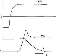 (a) Turn-off waveforms Generation-1 MCTs did not turn on rapidly in the vicinity of zero anode-cathode voltage and this posed a problem in softswitching applications of an MCT. However, Generation-2 MCTs have enhanced dynamic characteristics under zero voltage soft switching [16]. In an MCT, the PMOS On-FET together with the pnp transistor constitute a p-IGBT. An increase in the number of turn-on cells (decrease in the on-resistance of the p-IGBT) and an enhancement of their distribution across the MCT active area enable the MCT to turn on at a very low transient voltage allowing zero voltage switching (ZVS). During zero voltage turn-on, a bipolar device such as the MCT takes more time to establish conductivity modulation. Before the device begins to conduct fully, a voltage spike appears, thus causing a modest switching loss [12]. Reducing the tail-current amplitude and duration by proper circuit design can minimize the turn-off losses in softswitching cases. 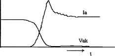 8.11.2 Resonant Converters Resonant and quasi-resonant converters are known for their reduced switching loss [17]. Resonant converters with zero current switching are built using MCTs and the circuit of one such, a buck-converter, is shown in Fig. 8.9. The resonant commutating network consisting of L, C, auxiliary switch T, and diode enables the MCT to turn off under zero current. The MCT must be turned off during the conduction period of D. Commutating switch must be turned off when the resonant current reaches zero. A resonant dc link circuit with twelve parallel MCTs has been reported [18]. In this circuit, the MCTs switch at zero-voltage instants. The elimination of the switching loss allows operation at higher switching frequencies, which in turn increases the power density and offers better control of the spectral content. The use of MCTs with the same forward drop provides good current sharing. FIGURE 8.8 switching. (b) Turn-on waveforms The MCT turn-off and turn-on waveforms under hard Soft-switching converters are being designed primarily to enable operation at higher switching frequencies. In these converters, the power devices switch at zero voltage or zero current, thereby eliminating the need for a large safe operating area (SOA) and at the same time eliminating the switching losses entirely. The MCT converters will outperform IGBT and power MOSFET converters in such applications by giving the highest possible efficiency. In soft-switching applications, the MCT will have only conduction loss, which is low and is close to that in a power diode with similar power ratings [12]. The / 14 Load FIGURE 8.9 Power circuit of MCT resonant buck-converter. The MCTs are also used in ac-resonant-link converters with pulse density modulation (PDM) [19]. The advantages of the PDM converter, such as zero-voltage switching, combined with those of the MCT make the PDM converter a suitable candidate for many ac-ac converter applications. In an ac-ac PDM converter, a low-frequency ac voltage is obtained by switching the high- frequency ac link at zero-crossing voltages. Two MCTs with reverse-connected diodes form a bidirectional switch that is used in the circuit. A single capacitor was used as a simple snubber for both MCTs in the bidirectional switch. Gate to Anode Voltage (Peak), У^ам ±20 V Rate of Change of Voltage (У^д = 15 V), dv/dt 10kV/is Rate of Change of Current, di/dt 80kA/is Peak Off-State Blocking Current (/drm) (Vj = -600 V = +15 V, Tc = +25°C) 200 iA On State Vohage (Vtm) (4 = 100 A, = -10 V Tc = +25°C) 1.3 V 8.12 Conclusions The MCT is a power switch with a MOS gate for turn-on and turn-off. It is derived from a thyristor by adding the features of a MOSFET. It has several advantages compared to modern devices such as the power MOSFET and the IGBT. In particular, the MCT has a low forward drop and a higher current density, which are required for high-power applications. The characteristics of Generation-2 MCTs are better than those of Generation-1 MCTs. The switching performance of Generation-2 MCTs is comparable to that of the IGBTs. However, with the development of high-speed IGBTs, it is yet to be seen which of the two devices wiU be dominant. Silicon Power Corporation is developing both PMCTs and NMCTs. A hybrid version of the MOS turn-off thyristor (MTOT) also is available. The data on MTOT and some preliminary data on PMCTs and NMCTs are available on the Internet. Acknowledgment The author is grateful to Ms. Jing He and Mr. Rahul Patil for their assistance in coUecting the reference material for this chapter. 8.13 Appendix The following is a summary of the specifications on a 600 V/ 150 A PMCT made by Silicon Power Corporation: Peak Off State Vohage, Vdrm - 600 V Peak Reverse Vohage, Vrrm +40 V Continuous Cathode Current, (T = +90°C), /к90 150A Non-Repetitive Peak Cathode Current, 4sm 5000 A Peak ControUable Current, /c 300 A Gate to Anode Voltage (Continuous), У^д +15V References 1. V. A. K. Temple, MOS-ControUed Thyristors -A new class of power devices, IEEE Trans, on Electron Devices 33: 1609-1618 (1986). 2. T. M. Jahns et a/., Circuit utilization characteristics of MOS-ControUed Thyristors, IEEE Trans, on Industry Applications 27:3, 589-597 (May/June 1991). 3. Harris Semiconductor, MCT/IGBTs/Diodes Databook 1995. 4. P. Holdman and F. Lotuka, SMPS IGBTs - High switching frequencies allow efficient switchers, PCIM Power Electronics Systems 25:2, 38-42 (February 1999). 5. D. Quek, Design of Protection and Control Strategies for Low-loss MCT Power Converters, Ph.D. Thesis, North Dakota State University, July 1994. 6. D. Quek and S. Yuvarajan, A novel gate drive for the MCT incorporating overcurrent protection, Proc. of IEEE IAS Annual Meeting 1994, pp. 1297-1302. 7. S. Yuvarajan, R. Nelson, and D. Quek, A study of the effects of snubber on switching loss and EMI in an MCT converter, Proc. of IEEE IAS Annual Meeting 1994, pp. 1344-1349. 8. T. C. Lee, M. E. Elbuluk, and D. S. Zinger, Characterization and snubbing of a bidirectional MCT switch in a resonant ac link converter, IEEE Trans. Industry Applications 31:5, 978-985 (Sept./Oct. 1995). 9. S. Yuvarajan and D. Quek, A PSPICE model for the MOS Controlled Thyristor, IEEE Trans, on Industrial Electronics 42:5, 554-558 (Oct. 1995). 10. G. L. Arsov and L. P. Panovski, An improved PSPICE model for the MOS-ControUed Thyristor, IEEE Trans. Industrial Electronics 46:2, 473-477 (April 1999). 11. R D. Kendle, V. A. K. Temple, and S.D. Arthur, Switching comparison of Generation-1 and Generation-2 P-MCTs and ultrafast N-IGBTs, Proc. of IEEE IAS Annual Meeting 1993, pp. 1286-1292. 12. E. Yang, V. Temple, and S. Arthur, Switching loss of Gen-1 and Gen-2 P-MCTs in soft-switching circuits, Proc. of IEEE APEC 1995, pp. 746-754. 13. Q. Huang et al, Analysis of n-channel MOS-ControUed Thyristors, IEEE Trans. Electron Devices 38:7, 1612-1618 (1991). 14. B. Jayant Baliga, Power Semiconductor Devices, PWS Publishing Co., Boston, 1996. 15. R. Rodrigues, A. Huang, and R. De Doncker, MTO Thyristor Power Switches, Proc. of PCIM97 Power Electronics Conference, pp. 4-1-4-12. 16. R. De Doncker et al, Characteristics of MOS-ControUed Thyristors 18. H.-R. Chang and A. V. Radun, Performance of 500 V, 450 A Parallel under zero voltage soft-switching conditions, IEEE Trans. Industry MOS Controlled Thyristors (MCTs) in a resonant dc-link circuit, Applications 28:2, 387-394 (March/April 1992). Proc. IEEE IAS Annual Meeting 1990, pp. 1613-1617. 17. A. Dmowski et al, Design of a buck converter with zero-current 19. M. E. Elbuluk, D. S. Zinger, and T. Lee, Performance of MCTs in a turn-off MCT, Proc. IEEE IAS Annual Meeting 1994, pp. 1025- current-regulated ac/ac PDM converter, IEEE Trans. Power Electro-1030. nics 11:1, 49-56 (January 1996). Static Induction Devices Bogdan M. Wilamowski, Ph.D. College of Engineering, University of Idaho, Boise, ID 83712 USA Summary................................................................................................... 127 9.1 Introduction...................................................................................... 127 9.2 Theory of Static Induction Devices........................................................ 128 9.3 Characteristics of Static Induction Transistor.......................................... 130 9.4 Bipolar Mode Operation of SI Devices (BSIT)........................................ 130 9.5 Emitters for Static Induction Devices..................................................... 131 9.6 Static Induction Diode (SID)............................................................... 131 9.7 Lateral Punch-Through Transistor (LPTT).............................................. 132 9.8 Static Induction Transistor Logic (SITE)................................................ 132 9.9 BJT Saturation Protected by SIT........................................................... 133 9.10 Static Induction MOS Transistor (SIMOS)............................................. 133 9.11 Space-Charge Limiting Load (SCLL)...................................................... 134 9.12 Power MOS Transistors....................................................................... 134 9.13 Static Induction Thyristor.................................................................... 135 9.14 Gate Turn-Off Thyristor (GTO)............................................................ 136 References.......................................................................................... 136 Summary Several devices from the static induction family including static induction transistors (SIT), static induction diodes (SID), static induction thyristors, lateral punch-through transistors (LPTT), static induction transistor logic (SITE), static induction MOS transistors (SIMOS), and space charge limiting load (SCLL) are described. The theory of operation of static induction devices is given for both a current controlled by a potential barrier and a current controlled by space charge. The new concept of a punch-through emitter (PTE), which operates with majority carrier transport, is presented. 9.1 Introduction Static induction devices were invented by Nishizawa [28]. The idea was so innovative that the estabhshment in the sohd-state electronics community at the time had difficulty understanding and accepting this discovery. Japan was the only country where static induction family devices were successfully fabricated [14]. The number of devices in this family continues to grow with time. Static induction transistors can operate with a power of 100 kW at 100 kHz or 10 W at 10 GHz. Static induction transistor logic had switching energy 100 x smaller than its IL competitor [8, 9]. The static induction thyristor has many advantages over the traditional SCR, and the static induction diode exhibits high switching speed, large reverse voltage, and low forward voltage drops. 9.2 Theory of Static Induction Devices The cross section of the static induction transistor is shown in Fig. 9.1, while its characteristics are shown in Fig. 9.2. An induced electrostatically potential barrier controls the current in static induction devices. The derivations of formulas will be done for an n-channel device, but the obtained results with a little modification also can be applied to p-channel devices. For a small electrical field existing in the vicinity of the potential barrier, the drift and diffusion current can be approximated by d(p(x) dn(x) (9.1) source о о о о о ate Note that the preceding equations derived for SIT also can be used to find current in any devices controUed by a potential barrier, such as a bipolar transistor or a MOS transistor operating in subthreshold mode, or in a Schottky diode. drain FIGURE 9.1 Cross section of the static induction transistor. where D = jVj and Vj = kT/q. By multiplying both sides of the equation by exp(-(p(x)/Vj) and rearranging n(x)exp( - (p(x) T / j (9.2) By integrating from Xi to one can obtain п(х2)ехр(-(р(х2)/Ут) - n(xi)exp(-(p(xi)/VT) Sexp(-cp(x)/Vr)dx With the foUowing boundary conditions (p(xi) = 0; n(xi) = Ns; (p(x2) = V; n(x2) = N; (9.3) (9.4) 9.3 Characteristics of Static Induction Transistor Samples of the potential distribution in SI devices are shown in Fig. 9.3 [1, 20]. The vicinity of the potential barrier was approximated by Plotka [11, 12] by using parabolic formulas (Fig. 9.4) along and across the channel. (p(x) = Ф (p(y) = Ф -(4-) (9.6) (9.7) Equation (9.3) reduces to Jn = lltxp{-cp{x)/Vr)dx (9.5) 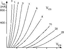 200- 200 400 600 800 11 FIGURE 9.2 Characteristics of the early SIT design [7]. FIGURE 9.3 Potential distribution in SIT: (a) view from the source side; and (b) view from the drain side. 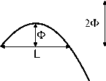  .0 2 4 6 Ф FIGURE 9.4 Potential distribution in the vicinity of the barrier approximated by parabolic shapes. Integrating Eq. (9.5) first along the channel and then across the channel yields a very simple formula for drain currents in /7-channel SIT transistors Ir, = qDpNsZ - exip (9.8) where Ф is the potential barrier height in reference to the source potential, is the electron concentration at the source, the W/L ratio describes the shape of the potential saddle in the vicinity of the barrier, and Z is the length of the source strip. As barrier height Ф can be a linear function of gate and drain voltages. Ir, = qDpNsZ - exipl--- (9.9) Equation (9.9) describes the characteristics of a static induction transistor for small current range. For large current levels the device current is controlled by the space charge of moving carriers. In the one-dimensional (ID) case the potential distribution is described by the Poisson equation: f(p p(x) SsiSo Av(x) (9.10) Where A is the effective device cross section and v(x) is carrier velocity. For a small electrical field v(x) = /лЕ(х) and the solution of Eq. (9.10) is DS - g DSlSiO -p (9.11) and for a large electrical field v(x) = const and Eq. (9.10) results in: DS - DS s2itSi0j2 (9.12) 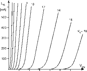 FIGURE 9.5 linear scale. 20 40 60 80 100 120 [v] Characteristics of the static induction transistor drawn in where L is the channel length and v 10 im/s is the carrier saturation velocity. In practical devices the current-voltage relationship is described by an exponential relationship Eq. (9.9) for small currents, a quadratic relationship eq. (9.11), and, finally, for large voltages by an almost linear relationship Eq. (9.12). The SIT characteristics drawn in linear and logarithmic scales are shown in Fig. 9.5 and Fig. 9.6, respectively. 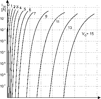 20 40 60 80 100 120 140 Vg [V] FIGURE 9.6 Characteristics of the static induction transistor drawn in logarithmic scale. 9.4 Bipolar Mode Operation of SI devices (BSIT) The bipolar mode of operation of SIT was first reported in 1976 by Nishizawa and Wilamowski [8, 9]. Several complex theories for the bipolar mode of operation were developed [2, 5, 6, 10, 23, 24], but actually the simple Eq. (9.5) works weU not only for the typical mode of the SIT operation, but also for the bipolar mode of the SIT operation. Furthermore, the same formula works very weU for classical bipolar transistors. Typical characteristics of the SI transistor operating in both normal and bipolar modes are shown in Figs. 9.7 and Fig. 9.8. A potential barrier controls the current in the SIT and it is given by qD Ns SxWi-(P(x)/Vj)dx (9.13) where (p(x) is the profile of the potential barrier along the channel. For example, in the case of npn bipolar transistors the potential distribution across the base in reference to emitter potential at the reference impurity level = Ng is described by: n] ) (9.14) DS AV =0.75V [ЦА] T ,GS 100 - 50 - 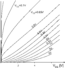 FIGURE 9.7 Small-sized SIT transistor characteristic, operating in both normal and bipolar modes, /д = /(Кд) with Vq as parameter. 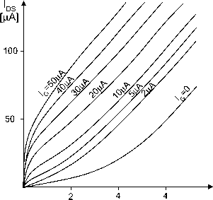 FIGURE 9.8 Small-sized SIT transistor characteristic, operating in both normal and bipolar modes, 4) = fiDs) ith as a parameter. After inserting Eq. (9.14) into (9.13) one can obtain the weU-known equation for electron current injected into the base qD r (9.15) If Eq. (9.13) is valid for SIT and BJT then one may assume that it is also valid for the bipolar mode of operation of the SIT transistor. This is a weU-known equation for the coUector current in the bipolar transistor, but this time it was derived using the concept of current flow through a potential barrier. 9.5 Emitters for Static Induction Devices One of the disadvantages of the SIT is the relatively flat shape of the potential barrier (Fig. 9.9a). This leads to slow, diffusion-based transport of carriers in the vicinity of the potential barrier. The carrier transit time can be estimated using the formula: Hransit ~ Y) (9.16) where /ff is the effective length of the channel and D = fiVis the diffusion constant. In the case of a traditional SIT transistor this channel length is 2 im, whUe in the case of SIT transistors with sharper barriers (Fig. 9.9b) the channel length is reduced to about 0.2 im. The corresponding transient times are 2 ns and 20 ps respectively. The potential distributions shown in Fig. 9.3 are valid for SIT with an emitter made of a traditional p-n junction. A much narrower potential barrier can be obtained when other types of emitter are used. There are two well-known emitters: (1) p-n junction (Fig. 9.10a); and (2) Schottky junction (Fig. 9.10b). For silicon devices p-n junctions have a forward voltage drop of 0.7-0.8 V while Schottky emitters have 0.2-0.3 V only. As the Schottky diode is a majority carrier device, carrier storage effect is negligible. Another interesting emitter structure is shown in Fig. 9.10c. This emitter has all the advantages of the Schottky diode even though it is fabricated out of p-n junctions. The concept of static induction devices can be used independently of the type of emitter shown in Fig. 9.10. With Schottky type and punch-through type emitters the potential barrier is much narrower and this results in faster response time and larger current gain in the bipolar mode of operation. FIGURE 9.9 Potential distributions in SIT: (a) traditional; and (b) with sharp potential barrier. FIGURE 9.10 Various structures of emitters: (a) p-n junction including heterostructure with SiGe materials; (b) Schottky junction; and (c) punch-through emitter (in normal operational condition the p region is depleted from carriers). 9.6 Static Induction Diode (SID) The bipolar mode of operation of SIT also can be used to obtain diodes with low forward voltage drop and negligible carrier storage effect [2, 5, 13, 23, 24]. A static induction diode can be obtained by shorting a gate to the emitter of the static induction transistor. Such a diode has all the advantages of a static induction transistor such as thermal stability and short switching time. The cross section of such a diode is shown in Fig. 9.11. anode emitter cathode FIGURE9.il section. Static induction diode: (a) circuit diagram; and (b) cross  Schotty cathode & & & i anode cathode anode FIGURE 9.12 Schottky diode with enlarged breakdown voltages: (a) circuit diagram; and (b) and (c) two cross-sections of possible implementation. The quality of the static induction diode can be further improved with more sophisticated emitters (Fig. 9.10b,c). The SI diode with Schottky emitter was described by Wilamowski in 1983 [17] (Fig. 9.12). A similar structure was later described by Baliga [1]. 9.7 Lateral Punch-Through Transistor (LPTT) Fabrications of SI transistors usually require very sophisticated technology. It is much simpler to fabricate a lateral punch-through transistor, which operates on the same principle and has similar characteristics [15]. The LPTT cross section is shown in Fig. 9.13 and its characteristics are shown in Fig. 9.14. 9.8 Static Induction Transistor Logic (SITL) The static induction transistor logic (SITL) was proposed by Nishizawa and Wilamowski [8, 9]. This logic circuit has almost 100 times better power-delay product than its PL 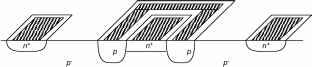 Drain Gate Emitter Gate Drain 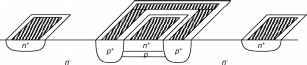 Drain Gate Emitter Gate Drain FIGURE 9.13 Structures of the lateral punch-through transistors: (a) simple; and (b) with sharper potential barrier.
20 40 60 DS FIGURE 9.14 Characteristics of lateral punch-through transistor. competitor. Such a great improvement of the power-delay product is possible because the SITL structure has a significantly smaUer junction parasitic capacitance and voltage swing is reduced. Figures 9.15 and 9.16 illustrate the concept of SITL. Measured characteristics of the n-channel transistor of the static induction logic are shown in Fig. 9.17. 9.9 BJT Saturation Protected by SIT The SI transistor also can be used instead of a Schottky diode to protect a bipolar junction transistor against saturation [20]. This leads to faster switching time. The concept is shown in Figs. 9.18 and 9.19. Note that this approach is advantageous to the solution with Schottky diode because it does not require additional area on a chip and does not introduce additional capacitance between the base and the coUector. The base 1 ... 10 11 12 13 14 15 16 ... 91 |
|
© 2026 AutoElektrix.ru
Частичное копирование материалов разрешено при условии активной ссылки |